jedec hbm带宽计算
- 格式:docx
- 大小:15.09 KB
- 文档页数:2

HBM测试方法本文旨在介绍《HBM测试方法》的目的和背景,并概述本文的结构。
HBM测试方法》是指针对电子产品进行人体静电放电(Human Body Model。
HBM)测试的方法。
HBM测试是一种常见的测试手段,用于评估电子设备在人体静电放电环境下的可靠性和安全性。
测试过程中,会模拟人体静电放电对电子产品可能造成的损害,并评估产品是否能够在此类环境下正常工作。
本文将首先介绍HBM测试的目的,即确定电子产品能否在人体静电放电环境下正常使用。
随后,将概述HBM测试的背景,包括该测试方法的起源和发展。
最后,将简要概述本文的结构,介绍后续各部分的内容和组织安排。
通过阅读本文,读者能够对《HBM测试方法》有一个基本的了解,并对其在电子产品可靠性和安全性评估中的重要性有所认识。
HBM(Human Body Model)测试是一种用于评估电子产品静电放电(ESD)抗性能的方法。
该方法模拟人体静电放电对电子产品可能造成的损害,以确保产品在正常使用时的可靠性。
HBM测试涉及以下几个方面:测试设备:HBM测试需要使用专门的测试设备,包括高阻抗电源、高电压放电控制器和模拟人体模型。
测试条件:HBM测试需要在恒温恒湿的环境下进行,以确保测试结果的准确性和可重复性。
测试环境应符合国际标准,如JESD22-A114.测试步骤:HBM测试包括以下步骤:准备测试样品:将待测产品放置在测试台上,并确保与测试设备连接良好。
设置测试参数:根据测试要求,设置合适的测试电流和放电时间。
进行放电测试:通过电压放电控制器模拟人体静电放电,并记录测试结果。
分析测试结果:根据测试结果评估测试样品的静电放电抗性能,包括放电幅度、放电时间和放电曲线等。
HBM测试方法能够帮助电子产品制造商评估产品的静电放电抗性能,以确保产品在正常使用时不会受到静电放电的损害,提高产品的可靠性和稳定性。
本文将介绍HBM测试的相关标准,包括国际标准和行业标准,并说明其重要性和适用范围。
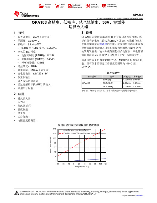
145125105856545255O f f s e t V o l t a g e (V )m -55-15525125Temperature (C)°-35456585105ProductFolder Order NowTechnical Documents Tools &SoftwareSupport &CommunityOPA188ZHCSB21B –MARCH 2013–REVISED SEPTEMBER 2016OPA188高精度、低噪声、轨至轨输出、36V 、零漂移运算放大器1特性•低失调电压:25μV (最大值)•零漂移:0.03μV/°C •低噪声:8.8nV/√Hz–0.1Hz 至10Hz 噪声:0.25μV PP •出色的DC 精度:–电源抑制比(PSRR);142dB –共模抑制比(CMRR):146dB –开环路增益:136dB •增益带宽:2MHz•静态电流:510μA (最大值)•宽电源电压:±2V 至±18V •轨至轨输出•输入包括负电源轨•已过滤射频干扰(RFI)的输入•微型尺寸封装2应用•桥式放大器•应力计•传感器应用•温度测量•电子称•医疗仪表•电阻温度检测器3说明OPA188运算放大器采用TI 的专有自动归零技术,以提供低失调电压(最大为25μV )并随时间推移和温度变化而实现接近零漂移的性能。
此高精度低静态电流微型放大器提供高输入阻抗和摆幅为电源轨15mV 之内的轨到轨输出。
输入共模范围包括负电源轨。
单电源或双电源可在4V 至36V (±2V 至±18V )范围内使用。
单通道版本采用微型SOT-23-5、MSOP-8和SO-8封装。
所有版本的额定工作温度范围均为-40°C 至+125°C 。
器件信息(1)器件型号封装封装尺寸(标称值)OPA188SOIC (8) 4.90mm x 3.91mm SOT-23(5) 2.90mm ×1.60mm VSSOP (8)3.00mm ×3.00mm(1)要了解所有可用封装,请参阅数据表末尾的封装选项附录。
![小度写范文[静电放电人体模型测试标准EIA/JEDEC中的问题研究] 静电放电人体模型hbm模板](https://img.taocdn.com/s1/m/4de2cdf4c77da26925c5b074.png)
[静电放电人体模型测试标准EIA/JEDEC中的问题研究] 静电放电人体模型hbm摘要:通过具体的实例说明目前的静电放电(Electrostatic Discharge,ESD)人体模型测试标准EIA/JEDEC尚存在一些需要完善的问题。
目前的标准EIA/JEDEC中缺少对起始测试电压的规定,导致有些测试直接从千伏(kV)量级的高压开始进行,造成一些设计不良的ESD防护器件在低压发生失效的状况可能被漏检的后果。
本文研究对象为一个漏端带N阱镇流电阻(Nwell-ballast)的GGNMOS(Gate-Grounded NMOS)型ESD防护结构。
用Zapmaster对它做人体模型(Human Body Model,HBM)测试,发现从1Kv起测时,能够通过8Kv的高压测试;而从50V起测时,却无法通过350V。
TLP测试分析的结果显示此现象确实存在。
本文详细剖析了该现象产生的机理,并采用OBIRCH失效分析技术对其进行了佐证。
因该问题具有潜在的普遍性,因此提出了对目前业界广泛采用的EIA/JEDEC测试标准进行补充完善的建议。
关键词:静电放电;人体模型;EIA/JEDEC 测试标准 A Case Study of Problems in EIA/JEDEC HBM ESD Test Standard HAN Yan, HUO Ming-xu, SONG Bo (ZJU-UCF Joint ESD Lab, Department of Information Science and Electronics Engineering, Zhejiang University, Hangzhou 310027,China)Abstract: There is a current need for modification of EIA/JEDEC Human-Body Model (HBM) Electrostatic Discharge (ESD) test standard, which does not define start and step test voltages. Some measurements start at several kilo-volts, which ignore that ESD protection devices might fail under low voltage stresses. A Gate-Grounded NMOS (GGNMOS) structure with an Nwell-ballast resistor connecting its drain and PAD is investigated for HBM ESD sustaining levels in this paper. When tested with a Zapmaster starting from 1 kilo-volts, the withstand voltage exceeds 8 kilo-volts, whereas the structure failed at 350 volts when the test initiates from 50 volts. The test results from a Transmission-Line Pulsing (TLP)system validate the phenomenon. The reason for the failure is also studied and confirmed with OBIRCH Failure Analysis (FA) results. To address this general issue, a suggestion for improving the present EIA/JEDEC HBM ESD test standard for industry applications is made. Key Words: Electrostatic Discharge, Human Body Model, EIA/JEDEC Test Standard 1引言随着微电子技术的发展和集成电路(Integrated Circuit, IC)工艺的进步,ESD引起的集成电路器件失效的几率越来越大,其防护设计引发业界的高度重视[1-3]。

2022 年 1 月,JEDEC 发布了新标准JESD238“高带宽内存 (HBM3) DRAM”。
与现有的 HBM2E 标准 (JESD235D) 相比,HBM3 标准提出了多项增强功能,包括支持更大的密度、更高速运算、更高的 Bank 数、更高的可靠性、可用性、可维护性 (RAS) 功能、低功耗接口和新的时钟架构。
HBM3 存储器很快就会被用于 HPC 应用,例如 AI、图形、网络,甚至可能用于汽车。
本文重点介绍了 HBM3 标准的一些关键功能,例如高容量、低功耗、改进的信道和时钟架构以及更先进的 RAS 选项。
图 1 中突出显示了一些关键功能。
图 1:HBM3 与 HBM2E 相比具有多项改进,包括更高的容量、更先进的 RAS 功能和更低的功耗更大、更快、更低功耗HBM2E标准的每个裸片的最大容量为2GB,每个堆栈可以放置12层裸片,从而可实现24GB的最大容量。
虽然标准是允许的,但我们尚未看到市场上出现任何 12 层的 HBM2E 堆栈。
HBM3 标准支持裸片的最大容量是4GB,以及高达 16 层的堆栈,总存储空间可以做到 64 GB,相比HBM2E有近 3 倍的增长。
Synopsys 预计 8 层和 12 层堆栈选项中的 16 GB 和 24 GB HBM3 器件很快就会上市。
为了支持更高密度的器件,HBM3 增加了从 12 层堆栈到 16 层堆栈的可用Bank 数,最多提供 64 个 Bank,增加了 16 个 Bank。
HBM3 标准的最高速度为 6.4 Gbps,几乎是 HBM2E 的最高速度 3.6 Gbps 的两倍。
在不久的将来,我们有理由期待第二代 HBM3 设备的出现。
只需看看HBM2/2E、DDR5(6400 Mbps 升级到 8400 Mbps)和 LPDDR5(最大速度为6400 Mbps,并快速让位于以 8533 Mbps 运行的 LPDDR5X)的速度历史记录,就可见一斑。

hbm jedec标准
HBM是高带宽内存的简称,它是用于高带宽存储器接口的内存规格,主要
应用于高性能计算、服务器、图形处理等领域。
HBM通过并行接口设计,
可以提供更高的内存带宽和容量,以支持大规模数据处理和高性能计算。
JEDEC是电子元件工业联合会(Joint Electron Device Engineering Council)的简称,它是一个国际性的电子设备标准制定组织,制定了许多
关于电子设备的设计、制造、测试和可靠性的标准。
其中,HBM标准就是
由JEDEC制定的一个标准。
HBM标准的制定是为了满足高性能计算和服务器领域对内存带宽和容量的
需求。
HBM通过将多个DRAM芯片堆叠起来,并通过先进的接口技术连接,实现了更高的带宽和容量。
HBM标准经过多次迭代,目前最新的是HBM3标准,它提供了更高的带宽和容量,以及更低的功耗和更高的可靠性。
总之,HBM和JEDEC标准都是为了满足高性能计算和服务器领域对内存带宽和容量的需求而制定的。
通过不断的技术创新和市场需求的推动,HBM
标准将不断演进和升级,以适应未来更高性能、更低功耗、更高可靠性的存储器市场需求。

ESD-HBM目标等级---liukanghui---背景20多年来,HBM (2 kV)和MM (200 V)的IC组件级ESD目标电平基本保持不变,没有更多数据来改变这些电平。
正如本文档中所显示的数据,OEMs所要求的今天增强的静态控制方法并不能证明这些更高的HBM/MM水平是合理的。
在当今最新的硅技术中,ESD过度设计到这种程度,越来越多地限制了硅的面积和性能,并导致产品创新周期更频繁地延迟。
HBM&MM 的ESD 要求回顾一直以来,HBM-2kV 仍然是一个安全“通过”电压目标。
当HBM 测试达到方法3015.7(1989)时,测试仪波形得到了很大的改进,但在这一点上,美国军方停止修改规范,并将HBM 规范的进一步开发转交给ESD 协会和JEDEC 的标准委员会HBM 目标水平动机人们首次对HBM 进行了系统测量(如惠普研究),包括坐在移动椅子上的人。
在第一届EOS/ESD 研讨会上发表了一些关于人体模型的早期工作的总结。
这些早期HBM 研究的工作人员发现,即使戴着腕带,也很容易产生1-2千伏的HBM20世20世纪70年代初汽车行业开始制定ESD 合格等级,福特采用了MM 和200 V ,通用汽车和克莱斯勒更关注HBM ,克莱斯勒在长时间考虑更高的电压后规定了2 kV HBM 的最低标准。
与此同时,RCA TV 部门决定采用2kv HBM 和专门设计的“显像管”测试模型,但没有人接受后者70年代和80年代初根据客户的这些要求,到20世纪80年代中期,半导体公司开始为组件制定内部HBM 标准,2KV HBM 规范成为其中最常见的规范20世纪80年代中期至于原因C, HBM 测试基本与现场的Overstress 破坏无关引入MM 动机a) MM 模拟了未接地的烙铁接触半导体引脚引线引起的故障。
b)此时MM 比HBM 更能模拟CDM 现场的损伤失效。
c)MM 模型中的零欧姆放电电阻导致热损伤的峰值电流高于HBM ,可以进行电压更低的MM 测试由于先进的自动化制造中ESD 控制的显著改善,原因A 不再存在原因B 也不再存在,因为较新的CDM 测试方法比MM 测试更好地再现了这些失败引入MM 动机ESD控制环境的变化和改进ESD历史处理程序早期•ESD控制程序已经实施了很多年。
GDDR和HBM新一代显存技术对比近年来,随着科技的快速发展,电子产品的性能要求也越来越高。
在图形处理和数据存储方面,高性能显卡和内存是不可或缺的组成部分。
GDDR(Graphics Double Data Rate)和HBM(High Bandwidth Memory)作为两种新一代显存技术,已经成为市场上主流的选择。
本文将对这两种显存技术进行对比,探讨它们的优势和不同之处。
1. 技术原理GDDR是一种专为图形处理器(GPU)设计的高带宽显存技术。
它采用了复杂的信号处理技术,在保持较低的功耗和低延迟的情况下实现了较高的数据传输速率。
GDDR通过并行传输技术,在相同频率下比传统的SDRAM(Synchronous Dynamic Random Access Memory)能够传输更多的数据。
HBM则是一种创新的高带宽内存架构。
它采用了通过硅基互联层将内存堆叠在一起的方式,实现了内存容量的大幅度增加和功耗的显著降低。
HBM利用高频率和并行传输方式,能够提供非常高的带宽和低延迟,适用于高性能计算和图形处理。
2. 带宽性能带宽是显存技术的一个重要指标,决定了显卡的数据传输速度和处理能力。
GDDR和HBM在带宽性能上有一些显著的差异。
GDDR技术在数据传输时能够实现较高的频率,从而获得较高的带宽。
GDDR5X甚至可以提供超过400GB/s的带宽,适用于大规模的图形计算和游戏。
HBM技术通过堆叠多个内存芯片来实现高带宽。
由于内存芯片的堆叠,HBM能够在较小的物理尺寸上提供更大的带宽。
例如,HBM2可以提供高达256GB/s的带宽,同时具有较低的延迟。
3. 性能功耗比性能功耗比是衡量显存技术优劣的另一个重要指标。
在同时满足高性能和低功耗的需求下,GDDR和HBM在性能功耗比上有所区别。
GDDR技术通过提高频率和并行传输的方式来提高数据传输速度,但功耗相对较高。
尽管GDDR能够提供高带宽,但其功耗也相应会增加,可能不适用于对功耗有严格要求的应用场景。
JEDECSTANDARD Electrostatic Discharge (ESD) Sensitivity Testing Human Body Model (HBM)JESD22-A114D(Revision of JESD22-A114C.01, March 2005)MARCH 2006JEDEC SOLID STATE TECHNOLOGY ASSOCIATIONNOTICEJEDEC standards and publications contain material that has been prepared, reviewed, and approved through the JEDEC Board of Directors level and subsequently reviewed and approvedby the JEDEC legal counsel.JEDEC standards and publications are designed to serve the public interest through eliminating misunderstandings between manufacturers and purchasers, facilitating interchangeability and improvement of products, and assisting the purchaser in selecting and obtaining with minimum delay the proper product for use by those other than JEDEC members, whether the standard is tobe used either domestically or internationally.JEDEC standards and publications are adopted without regard to whether or not their adoption may involve patents or articles, materials, or processes. By such action JEDEC does not assume any liability to any patent owner, nor does it assume any obligation whatever to parties adoptingthe JEDEC standards or publications.The information included in JEDEC standards and publications represents a sound approach to product specification and application, principally from the solid state device manufacturer viewpoint. Within the JEDEC organization there are procedures whereby a JEDEC standard or publication may be further processed and ultimately become an ANSI/EIA standard.No claims to be in conformance with this standard may be made unless all requirements stated inthe standard are met.Inquiries, comments, and suggestions relative to the content of this JEDEC standard or publication should be addressed to JEDEC at the address below, or call (703) 907-7559 orPublished by©JEDEC Solid State Technology Association 20062500 Wilson BoulevardArlington, VA 22201-3834This document may be downloaded free of charge; however JEDEC retains thecopyright on this material. By downloading this file the individual agrees not tocharge for or resell the resulting material.PRICE: Please refer to the currentCatalog of JEDEC Engineering Standards and Publications online at/Catalog/catalog.cfmPrinted in the U.S.A.All rights reservedJEDEC Standard No. 22-A114DPage 1Test Method A114D(Revision of Test Method A114C.01)TEST METHOD A114DELECTROSTATIC DISCHARGE (ESD) SENSITIVITY TESTINGHUMAN BODY MODEL (HBM)(From JEDEC Board Ballot JCB-00-27, JCB-04-103, JCB-04-104, JCB-04-105, JCB-05-137, and JCB-05-138 formulated under the cognizance of JC-14.1 Committee on Reliability Test Methods for Packaged Devices.)1 ScopeThis method establishes a standard procedure for testing and classifying microcircuits according to their susceptibility to damage or degradation by exposure to a defined electrostatic Human Body Model (HBM) discharge (ESD). The objective is to provide reliable, repeatable HBM ESD test results so that accurate classifications can be performed.2 ApparatusThis test method requires the following equipment. 2.1 An ESD pulse simulator and a Device Under Test (DUT) socket equivalent to the circuit ofFigure 1. The simulator must be capable of supplying pulses with the characteristics required by Figure 2 and Figure 3.2.2 OscilloscopeThe oscilloscope and amplifier combination shall have a 350 MHz minimum single-shot bandwidth and a visual writing speed of 4 cm/ns minimum. 2.3 Current probeThe current probe shall have a minimum pulse-current bandwidth of 350 MHz. The probe (transformer and cable with a nominal length of 1 meter) shall have a 1 GHz bandwidth, a minimum current rating of 12 amperes peak pulse-current capability and a rise time of less than one nanosecond.2.4 Evaluation loadsAn 18-24 AWG tinned copper wire is recommended for the short waveform verification test. The lead length should be as short as practicable to span the distance between the two farthest pins in the socket while passing through the current probe. The ends of the wire may be ground to a point where clearance is needed to make contact on fine-pitch socket pins.A 500 Ω +/-1%, 4000 V, low-inductance resistor shall be used for initial system checkout and periodic system recalibration.JEDEC Standard No. 22-A114D Page 2Test Method A114D(Revision of Test Method A114C.01)2 Apparatus (cont’d)2.5 CalibrationAll apparatus used for tester evaluation shall be calibrated according to a documented, traceable calibration system and in accordance with manufacturer’s recommendations.Figure 1 — Typical equivalent HBM ESD circuitNOTE 1 The performance of any simulator is influenced by its parasitic capacitance and inductance.NOTE 2 Precautions must be taken in tester design to avoid recharge transients and multiple pulses.NOTE 3 R2, used for initial equipment qualification and requalification as specified in 3.1, shall be a low inductance, 4000 V, 500 Ω resistor with +/-1% tolerance.NOTE 4 Stacking of DUT socket adaptors (piggybacking) is allowed only if the waveforms can be verified to meet the specifications in Table 1.NOTE 5 Reversal of terminals A and B to achieve dual polarity is not permitted.NOTE 6 S2 shall be closed at least 10 milliseconds after the pulse delivery period to ensure the DUT socket is not left in a charged state.NOTE 7 R1, 1500 Ω +/- 1%.NOTE 8 C1, 100 pF +/- 10% (effective capacitance).JEDEC Standard No. 22-A114DPage 3Test Method A114D(Revision of Test Method A114C.01)2 Apparatus (cont’d)(a) Pulse rise time, (t r )(b) Pulse decay time, (t d )Figure 2 — Current waveforms through a shorting wireI ps36.8%JEDEC Standard No. 22-A114D Page 4Test Method A114D(Revision of Test Method A114C.01)2 Apparatus (cont’d)Figure 3 — Current waveform through a 500 Ω resistor** The 500 Ω load is used only during Equipment Qualification as specified in 3.1. 2.6 Optional trailing pulse detection apparatusThe following are required to conduct the optional trailing pulse detection in Figure 4.1. A voltage probe with a minimum input impedance of 10M Ω, a maximum capacitance of 10 pF, a minimum bandwidth of 1 MHz, and a minimum peak-to-peak voltage rating of 15 V.2. A 10k Ω +/- 1%, 4000 V resistor.3. A Zener diode with breakdown voltage between 6 V and 15 V and a rating between ¼ watt and 1 watt.JEDEC Standard No. 22-A114DPage 5Test Method A114D(Revision of Test Method A114C.01)2 Apparatus (cont’d)Measurement setup:-load = 10k ohm-parallel Zener diode (Vbd ~ 10V) for probe/scope protectionmain ESD pulse (off scale)second ESD pulse (off scale)trailing pulseAt 2 kVFigure 4 — Measurement setup and typical voltage waveform for detecting trailing EOS pulse(optional) 3Qualification, calibration, and waveform verification3.1 Equipment qualificationEquipment calibration must be performed during initial acceptance testing. Recalibration is required whenever equipment repairs are made that may affect the waveform and a minimum of every 12 months. The tester must meet the requirements of Table 1 and Figure 2 at all voltage levels, except 8000 V, using the shorting wire and at the 1000 V and 4000 V levels with the 500 Ω resistor (see Figure 3). The 8000 V level is optional. The waveform measurements during calibration shall be made using the worst-case pin on the highest pin count board with a positive mechanical clamp socket. (Machine repeatability should be verified during initial equipment acceptance by performing a minimum of 5 consecutive positive and a minimum of 5 consecutive negative waveforms at a voltage level in Table 2.)The high-voltage relays and associated high-voltage circuitry shall be tested by the user of computer-controlled systems per the equipment manufacturer's instructions (system diagnostics). This test will check for any open or short relays.JEDEC Standard No. 22-A114D Page 6 Test Method A114D(Revision of Test Method A114C.01)3 Qualification, calibration , and waveform verification (cont’d)Table 1 — Waveform SpecificationVoltage Level (V) Ipeak for Short†, Ips (A) Ipeak for 500 Ω* Ipr (A) Rise Timefor Short, t r(ns) Rise Time for 500 Ω* t rr (ns) Decay Time for Short, t d (ns)Ringing Current I R (A) 250 0.15-0.19 N/A 2.0-10 N/A 130-170 15% of Ips 500 0.30-0.37 N/A 2.0-10 N/A 130-17015% of Ips1000 0.60-0.74 0.37-0.55 2.0-10 5.0-25 130-17015% of Ips2000 1.20-1.48 N/A 2.0-10 N/A 130-17015% of Ips4000 2.40-2.96 1.5-2.2 2.0-10 5.0-25 130-17015% of Ips and Ipr 8000 (optional)4.80-5.86N/A2.0-10N/A130-17015% of Ips† Ipeak is the current through R1, that is, approximately V/1500 Ω.* The 500 Ω load is used only during equipment qualification as specified in 3.1.3.1.1 Safety trainingDuring initial equipment set-up, the safety engineer or applicable safety representative, shall inspect the equipment in its operating location to ensure that the equipment is not operated in a combustible (hazardous) environment.Additionally, all personnel shall receive system operational training and electrical safety training prior to using the equipment.JEDEC Standard No. 22-A114DPage 7Test Method A114D(Revision of Test Method A114C.01)3 Qualification, calibration, and waveform verification (cont’d)3.1.2 Detection of trailing EOS pulse (optional)Some HBM testers are known to produce a trailing electrical pulse. Some advanced technologies may be vulnerable to these pulses resulting in an electrical overstress (EOS). If trailing pulses are of concern for the technology under test, then any trailing pulse after the HBM pulse must be less than 4 μA at positive and negative 4000 V level using the 10 k Ω load in parallel with the Zener diode, as shown in Figure 4. Scanning for the presence of any trailing pulse shall cover a period of at least 1 msec after the HBM pulse.NOTE 1 The HBM pulse may show a slow decay of up to 100 μsec to reach the 4 μA specification level due to the use of a large load and the added capacitive parasitics in the measurement setup. This part of the slow decay shall be excluded in determining the trailing pulse magnitude.NOTE 2 To determine if a device to be tested is susceptible to damage from the trailing pulse it may be necessary to measure the voltage across the actual device during HBM testing, or a circuit similar to that in Figure 4. If the circuit in Figure 4 is used the resistor should be changed from the 10 k Ω value to a value that simulates the device’s properties and the Zener diode should be chosen to match the device’s breakdown voltage. The measured voltage and the time that it is present on the device can then be compared to the known reliability mechanisms of thetechnology, such as time dependent dielectric breakdown (TDDB), to determine if a reliability concern is posed by the HBM tester. For sufficiently advanced technologies it may be necessary to use a criterion more stringent than the 4 μA at 4000 V with a 10 k Ω resistor.3.2 Worst-case pinThe worst-case pin combination for each socket and DUT board shall be identified and documented. It is recommended that the manufacturers supply the worst-case pin data with each DUT board. The pin combination with the waveform closest to the limits (see Table 1) shall be designated for waveform verification.3.2.1 The worst-case pin combination shall be identified by the following procedure.3.2.1.1 For each test socket, identify the socket pin with the shortest wiring path from the pulsegenerating circuit to the test socket. Connect this pin to Terminal B (where it will remain the referenced pin throughout the worst-case pin search) and connect one of the remaining pins to Terminal A. Attach a shorting wire between these pins with the current probe around the shorting wire, as close to Terminal B as practicable.3.2.1.2 Apply at least one positive 4000 V pulse and at least one negative 4000 V pulse and verify that the waveform meets the requirements defined in Table 1 for both positive and negative pulses.3.2.1.3 Repeat steps 3.2.1.1 and 3.2.1.2 until all socket pins have been evaluated.3.2.1.4 Determine the worst-case pin pair (within the limits and closest to the minimum or maximum parameter values as specified in Table 1) to be used for future waveform verification.JEDEC Standard No. 22-A114D Page 8Test Method A114D(Revision of Test Method A114C.01)3.2 Worst-case pin (cont’d)3.2.1.5 For initial board check-out connect a 500 Ω resistor between the worst-case pins previously identified with the shorting wire in step 3.2.1.4. Apply a positive and negative 4000 V pulse and verify that the waveform meets the requirements defined in Table 1.NOTE As an alternative to the worst-case pin search, the reference pin pair may be identified for each test socket of each test fixture. The reference pin combination shall be identified by determining the socket pin with the shortest wiring path from the pulse generating circuit to the test socket. Connect this pin to Terminal B and then connect the socket pin with the longest wiring path from the pulse generating circuit to the test socket to Terminal A (normally provided by the manufacturer). Attach a shorting wire between these pins with the current probe around the shorting wire. Follow the procedure in step 3.2.1.2. For the initial board check-out connect a 500 Ω resistor between the reference pins. Apply a positive and negative 4000 V pulse and verify the waveform meets the requirements defined in Table 1.3.3 Waveform verificationThe waveform verification should be performed at the beginning of each shift that a tester is operated and when a socket/DUT board is changed. If at any time the waveforms do not meet the requirements defined within Figure 2 and Table 1 at the 1000 V or 4000 V level, the testing shall be halted until the waveform is in compliance. Additionally, the system diagnostics test as defined in 3.1 for automated systems shall be performed prior to the beginning of each shift testing is done. The period between waveform checks may be extended providing test data supports the increased interval. In case the waveform no longermeets the limits in Table 1, all ESD testing performed after the previous satisfactory waveform check will be considered invalid.a) With the required DUT socket installed and with no part in the socket, attach a shorting wire in theDUT socket such that the worst-case pins are connected between Terminal A and Terminal B as shown in Figure 1. Place the current probe around the shorting wire.b) Initiate at least one positive pulse at the 1000 V level per Table 1 and Figure 2. Verify that allparameters meet the limits specified in Table 1 and Figure 2.c) Initiate at least one negative pulse at the 1000 V level per Table 1. Verify that all parameters meet thelimits specified in Table 1 and Figure 2.d) Initiate at least one positive pulse at the 4000 V level per Table 1 and Figure 2. Verify that allparameters meet the limits specified in Table 1 and Figure 2.e) Initiate at least one negative pulse at the 4000 V level per table 1. Verify that all parameters meet thelimits specified in Table 1 and Figure 2.JEDEC Standard No. 22-A114DPage 9Test Method A114D(Revision of Test Method A114C.01)4 Classification procedureThe devices used for classification testing must have completed all normal manufacturing operations. Testing must be performed using an actual device chip. It is not permissible to use a test chiprepresentative of the actual chip or to assign threshold voltages based on data compiled from a design library or via software simulations.NOTE Test chip in this case means ESD test structure.4.1 Parametric and functional testingPrior to ESD testing, parametric and functional testing using conditions required by the applicable part drawing or test specification shall be performed on all devices submitted for ESD testing. Guard band testing is also permitted. The test devices shall be within the limits stated in the part drawing for these parameters. 4.2 Devices for each voltage levelA sample of 3 devices for each voltage level shall be characterized for the device ESD failure threshold using the voltage steps shown in Table 1. Finer voltage steps may optionally be used to obtain a more accurate measure of the failure threshold. ESD testing should begin at the lowest step in Table 1 but may begin at any level. However, if another higher starting voltage level is used and the device fails, testing shall be restarted with a fresh device at the next lowest level. The ESD test shall be performed at room temperature. 4.3 Stress levelEach sample of 3 devices shall be stressed at one voltage level using 1 positive and 1 negative pulse with a minimum of 100 milliseconds between pulses per pin for all pin combinations specified in Table 2. Longer intervals are permitted and should be used if the devices are expected to be vulnerable tocumulative effects. It is permitted to use a separate sample of 3 devices for each pin combination set specified in Table 2. It is permitted to further partition each pin combination set in Table 2 and use a separate sample of 3 devices for each subset within the pin combination set. It is permitted to use the same sample (3) at the next higher voltage stress level if all parts pass the failure criteria specified in clause 5 after ESD exposure to a specified voltage level.4.4 Pin combinationsThe pin combinations to be used are given in Table 2. The actual number of pin combination sets depends on the number of power pin groups. Power pins and Power Pin Groups are defined in 4.5. Programming pins that do not draw current should be considered as I/O pins (example: Vpp pins on memory devices). Active discrete devices (FETs, transistors, etc.) shall be tested using all possible pin-pair combinations (one pin connected to Terminal A, another pin connected to Terminal B) regardless of pin name or function. All pins which are not connected to the die shall be verified as such and left open (floating) at all times. Pins labeled as “no connect” that are electrically connected to the die shall be tested as non-supply I/O pins.JEDEC Standard No. 22-A114D Page 10 Test Method A114D(Revision of Test Method A114C.01)4 Classification procedure (cont’d)4.5 Power pinsA power pin is defined as any pin intended to provide power to any portion of the circuit. While most power pins are labeled such that they can be easily recognized as power pins (examples: VDD, VDD1, VDD2, VDD_PLL, VCC, VCC1, VCC2, VCC_ANALOG, VSS, VSS1, VSS2, VSS_PLL,VSS_ANALOG, etc.), others are not and require engineering judgment based on their functions in the normal circuit operation (examples: Vbias, Vref, etc.).Power pins that are directly connected by metal (inside the package) form a power pin group.4.5.1 Power pins connected on diePower Pin Groups that are connected by metal at the die level may be tied together and treated as a single node for Terminal B connection but must be treated as individual pins for Terminal A as shown in Table 2.4.5.2 Power pins connected on package planeFor Power Pin Groups that are tied together through a common package plane, it is permitted to select one or more (arbitrary) pins to represent the group for stressing (Terminal A). The other pins in the group do not need to be stressed. In the test sequences where this power pin group is held at ground (Terminal B), it is permitted to have all the pins in the group tied together and connected to Terminal B or to have only the previously selected pin(s) connected to Terminal B with all other pins in the group left floating.4.5.3 Other power pin typesAny pin that is intended to be pumped above the positive supply or below the negative supply of itscircuit block must be treated as a power pin (example: positive and negative terminal pins connected to a charge pump capacitor).Any pin that is connected to an internal power bus (or a power pin) by metal must be treated as a power pin (example: a Vdd sensing pin). In that case, the pin may be tied together with the power pin(s) connected to the same bus and treated as one pin for Terminal B connection even though it is labeled a different name.Any pin that is intended to supply power to another circuit on the same chip must be treated as a power pin. However, if a pin intended to supply power to a circuit on another chip but not to any circuit on the same chip, it may be treated as a signal pin. 4.6 I/O to I/OIf a device has non-supply pins that are connected on the die and bonded out to multiple separate pins, then these pins shall be stressed individually according to combination set N+1 with the remainder of these connected pins left floating.JEDEC Standard No. 22-A114DPage 11Test Method A114D(Revision of Test Method A114C.01)4 Classification procedure (cont’d) 4.6 I/O to I/O (cont’d)Pin combination set N+1 in table 2 specifies to stress each non-supply pin individually with all other remaining non-supply pins tied together and connected to terminal B (except for those non-supply pins that are metal connected to the pin under stress on the die, which will be left open). As an alternative to this method, it is permitted to partition the pins to be connected to terminal B into two or more subsets, such that each of these pins is a member of at least one subset. The pin connected to terminal A is to be stressed to each of these subsets separately. 4.7 Alternative sample groupIf a different sample group is ESD tested at each stress level, it is permitted to perform the dc parametric and functional ATE testing after all sample groups have been ESD tested.Table 2 — Pin Combinations Sets for Integrated CircuitsPin Combination Set Connect Individually to Terminal A Connect to Terminal B (Ground) Floating Pins (unconnected)1 All pins one at a time, except the pin(s) connected to Terminal BFirst power pin group All pins except PUT* and first power pin group2 All pins one at a time, except the pin(s) connected to Terminal BSecond power pin group All pins except PUT and secondpower pin group3 All pins one at a time, except the pin(s) connected to Terminal B Nth power pin group All pins except PUT and Nth powerpin group4 Each Non-supply pin, one at a time. All other Non-supply pins collectively except PUT All power pins(see 4.6)* PUT = Pin under test.JEDEC Standard No. 22-A114D Page 12Test Method A114D(Revision of Test Method A114C.01)5 Failure criteriaA part will be defined as a failure if, after exposure to ESD pulses, it no longer meets the part drawing requirements using parametric and functional testing. If testing is required at multiple temperatures, testing shall be performed at the lowest temperature first.6 Classification criteriaAll samples used must meet the test requirements of section 4 up to a particular voltage level in order for the part to be classified as meeting a particular sensitivity classification.CLASS 0: Any part that fails after exposure to an ESD pulse of 250 V or less.CLASS 1A: Any part that passes after exposure to an ESD pulse of 250 V but fails after exposure to anESD pulse of 500 V.CLASS 1B: Any part that passes after exposure to an ESD pulse of 500 V, but fails after exposure to anESD pulse of 1000 V.CLASS 1C: Any part that passes after exposure to an ESD pulse of 1000 V, but fails after exposure toan ESD pulse of 2000 V.CLASS 2: Any part that passes after exposure to an ESD pulse of 2000 V, but fails after exposure toan ESD pulse of 4000 V.CLASS 3A: Any part that passes after exposure to an ESD pulse of 4000 V, but fails after exposure toan ESD pulse of 8000 V.CLASS 3B: Any part that passes after exposure to an ESD pulse of 8000 V.JEDEC Standard No. 22-A114DPage 13 Annex A (informative) Differences between JESD22-A114D and JESD22-A114C.01This table briefly describes most of the changes made to entries that appear in this standard,JESD22-A114D, compared to its predecessor, JESD22-A114C.01 (March 2005). If the change to a concept involves any words added or deleted (excluding deletion of accidentally repeated words), it is included. Some punctuation changes are not included.Page Description of change9 In 4.4 changed last sentence from “All pins configured as “no connect” shall be tested asnon-supply I/O pins.”, to “All pins which are not connected to the die shall be verified assuch and left open (floating) at all times. Pins labeled as “no connect” that are electricallyconnected to the die shall be tested as non-supply I/O pins.”10 In 4.5, second paragraph, removed “may be tied together and treated as one pin for Terminal Bconnection. Otherwise each power pin must be treated as a separate power pin.” , replaced with“form a power pin group.”10 In 4.5, last three paragraphs became 4.5.3.10 Added 4.5.1 and 4.5.210 New 4.6 added, 4.6 became 4.7.11 Table 2 in 3rd and 4th columns; changed “pin(s)” to “pin groups”.A.1 Differences between JESD22-A114C.01, compared to its predecessor, JESD22-A114C(January 2005)Page Description of change3 Figure 3b was deleted. It was approved for removal in the publication of JESD22-A114C, this was missed at the time of publication.A.2 Differences between JESD22-A114C, compared to its predecessor, JESD22-A114-B (June2000).Page Description of change3 Figure 2b was modified to show pulse decay time definition more clearly3 Figure 3b was deleted since it is not used.4 Inserted 2.6 to describe the equipment required for Trailing Pulse.5 Figure 4 has been added to show the test set-up for Trailing EOS Pulse.7 Inserted 3.1.2 to describe the test and give guidance on its applicability.9 Added in 4 language stating clearly that ESD testing must be performed on samples ofthe actual chip being evaluatedTest Method A114D(Revision of Test Method A114C.01)JEDEC Standard No. 22-A114DPage 14A.2 Differences between JESD22-A114C, compared to its predecessor, JESD22-A114-B (June2000). (cont’d)Page Description of change9 In 4.3: Reduced minimum interval between zaps to 100 milliseconds. Longer intervalsare still permitted.9 In 4.3: Clarified that pin combination sets may be partitioned as far as necessary andperformed on different devices to eliminate possible cumulative effects.9 In 4.4: the following text was removed: “Like named power pins (VCC1, VCC2, VSS1,VSS2, GND, etc.) that are directly connected by metal (inside the package) may be tiedtogether and treated as one pin for Terminal B connection. Otherwise, each power pinmust be treated as a separate power pin.” and replaced with “Power pins are defined in4.5.”9 In 4.4: the following text was removed: “All pins configured as "no connect" pins shallbe verified as “no connect” and left open (floating) at all times. Pins labeled “noconnect”, that in fact are connected, shall be tested as non-supply pins.” and replacedwith “All pins configured as “no connect” shall be tested as non-supply I/O pins.”10 Added 4.5: Clarified power pin definitions. Included pins connected to charge pumpcapacitors as power pins.Test Method A114D(Revision of Test Method A114C.01)。
密级:受控HMC_HBM技术分析摘要:涉及HMC及HBM新兴内存技术分析。
关键字:HMC,HBM,3D内存目录0 引言 (5)1 What (5)1.1 HMC概述 (5)1.2 HMCC概述 (6)1.3 HMC技术概述 (7)1.4 TVS硅穿孔技术 (8)1.5 HMC上的逻辑芯片 (9)1.6 HMC与其他内存比较 (10)2 When (13)3 Where (13)4 Who (14)4.1 Micron (14)4.1.1 芯片规格及状态 (14)4.1.2 芯片架构 (15)4.1.3 芯片应用拓扑 (15)4.1.4 芯片特性--HMC1.0 (17)4.1.5 芯片特性--HMC2.0 (17)4.2 Altera (18)4.2.1开发板 (18)4.2.2 IP核 (20)4.2.3 Altera HMC Roadmap (21)4.3 Xilinx (21)4.3.1 Xilinx与Open-Silicon的HMC ip 核 (21)4.3.2 Xilinx与Pico Computing的HMC ip核 (22)4.4 Intel (22)4.5 Juniper (23)5 Why (24)6 How (25)6.1 HBM与HMC较量一 (25)6.2 HBM与HMC较量二 (26)7 价值点 (26)7.1 带宽:比DDR3快15倍 (26)7.2 容量:比DDR3大2倍以上 (27)7.3 体积:比DDR3少90% (27)7.4 功耗:每bit功耗比DDR3少70% (29)7.5 结论 (29)参考文献 (29)0 引言下文将以HMC来论述。
1 What1.1 HMC概述Hybrid Memory Cube,HMC,混合存储立方体/混合内存立方体。
HMC已被行业领导者和有影响力的人士视为一项万众期待的技术方案,它突破了传统内存技术所受限制,在提供超高系统性能的同时显著减少了每比特耗电量。
jedec hbm带宽计算
JEDEC HBM(High Bandwidth Memory)是一种高带宽内存技术,用于提供高性能的图形处理器和加速器。
要计算JEDEC HBM的带宽,需要考虑以下几个因素:
1. 数据总线宽度,JEDEC HBM标准定义了每个通道的数据总线
宽度,通常为128位或256位。
数据总线宽度越大,带宽越高。
2. 时钟频率,JEDEC HBM规范中定义了内存的工作频率,通常
以MHz为单位。
时钟频率越高,数据传输速度越快,带宽也会相应
增加。
3. 通道数量,HBM内存通常有多个通道,每个通道都有自己的
数据总线。
通道数量的增加会直接提高带宽。
带宽的计算公式为,带宽 = 数据总线宽度× 时钟频率× 通
道数量 / 8。
需要注意的是,这里的数据总线宽度和时钟频率需要
以相应的单位进行转换,以便在公式中得到正确的带宽单位(通常
为GB/s)。
举例来说,假设JEDEC HBM内存的数据总线宽度为256位,时钟频率为1.6 GHz,通道数量为4,则带宽计算公式为,带宽 = 256 × 1.6 × 4 / 8 = 256 GB/s。
通过以上公式和例子,可以计算出JEDEC HBM的带宽。
当然,在实际应用中,还需要考虑其他因素,如延迟、数据传输模式等,以全面评估内存的性能特征。
希望这个回答能够帮助你理解JEDEC HBM带宽的计算方法。