
GRM219R61C475K中文资料
- 格式:pdf
- 大小:34.88 KB
- 文档页数:1
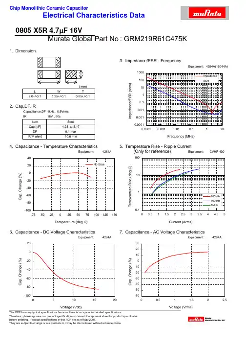

物料编号:GRM155R61A475KEAAD详细参数_易容网
MLCC即是多层陶瓷电容片式,是电子信息产品不可或缺的基本组件之一。
我国MLCC的生产起步在80年代初,行业早期主要是在外资企业的带动下发展起来的,近年来国内企业在技术上实现突破,行业国产化成效显著,并推动了MLCC产量迅速增长。
目前,MLCC的应用领域已从手机、电脑、电视机等消费电子领域,逐步拓展到新能源发电、新能源汽车、节能灯具、轨道交通、直流输变电、三网融合、高清电视、机顶盒、手机电视等多个行业。
对于这个悄悄活跃在人们生活中的元件你又知道多少呢.
本次易容网为大家推荐比较常用的MLCC村田 | Murata品牌的料号GRM155R61A475KEAAD的相关参数
易容网是深圳市易容信息技术有限公司独自研发的全球最大的MLCC搜索采购服务网站,2014年创立于深圳市南山区,全国首家电子元器件行业电容元件的搜索引擎及o2o商务服务平台。
易容网()现已建成全球最大的MLCC电容搜索引擎数据库,包含全球25家电容生产厂商超过28万组MLCC产品数据,用户可根据行业应用、物料编号、规格参数等信息快速的找到所有相关的MLCC电容数据。
易容网在搜索服务的前提下还提供村田、TDK、国巨、太阳诱电、风华高科等常见品牌产品的o2o商务服务,让企业客户实现询价、报价、在线订单、出库、实时物流、签收、账期服务等在线一站式商务服务体验。


FEATURES DESCRIPTIONAPPLICATIONSTYPICAL APPLICATIONGNDLVINSSFBTOP VIEWC1: Murata GRM188R60J105K R3: Noise decoupling resistorC2: Murata GRM219R61C475K Cs: Soft start programming capacitorTPS61080TPS61081SLVS644B–FEBRUARY2006–REVISED JANUARY2007 HIGH VOLTAGE DC/DC BOOST CONVERTER WITH0.5-A/1.3-A INTEGRATED SWITCH• 2.5-V to6-V Input Voltage Range The TPS61080/1is a 1.2MHz/600kHz fixedfrequency boost regulator designed for high •Up to27-V Output Voltageintegration,which integrates a power switch,an •0.5-A Integrated Switch(TPS61080)input/output isolation switch and a power diode.1.3-A Integrated Switch(TPS61081)When a short circuit condition is detected,the •12V/400mA and24V/170mA From5-V Input isolation switch opens up to disconnect the output (TYP)from the input.As a result,the IC protects itself andthe input source from any pin,except VIN,from •Integrated Power Diodebeing shorted to ground.The isolation switch also • 1.2-MHz/600-kHz Selectable Fixed Switching disconnects the output from input during shutdown toFrequency prevent any leakage current.Other provisions for •Input to Output Isolation protection include0.5A/1.3A peak-to-peak overcurrent protection,programmable soft start(SS),•Short-Circuit Protectionover voltage protection(OVP),thermal shutdown and •Programmable Soft Start under voltage lockout(UVLO).•Overvoltage ProtectionThe IC operates from input supplies including single •Up to87%Efficiency Li-ion battery,triple NiMH,and regulated5V,such as•10-Pin3mm×3mm QFN Package USB output.The output can be boosted up to27V.TPS61080/1can provide the supply voltages ofOLED,TFT-LCD bias,12V and24V power rails.Theoutput of TPS61080/1can also be configured as a • 3.3V to12V,5V to12V and24V Boostcurrent source to power up to7WLED in flash light Converterapplications.•White LED Backlight for Media Form FactorDisplayORDERING INFORMATION•OLED Power SupplyT A OVERCURRENT PACKAGE PACKAGE •xDSL Applications LIMIT MARKING•TFT-LCD Bias Supply0.5A(min)TPS61080DRCR BCN•White LED Flash Light 1.3A(min)TPS61081DRCR BCO–40°Cto85°C0.5A(min)TPS61080DRCT BCN1.3A(min)TPS61081DRCT BCOFigure1.5V to12V,250mA Step-Up DC/DCConverterPlease be aware that an important notice concerning availability,standard warranty,and use in critical applications of TexasInstruments semiconductor products and disclaimers thereto appears at the end of this data sheet.PowerPAD is a trademark of Texas Instruments.PRODUCTION DATA information is current as of publication date.Copyright©2006–2007,Texas Instruments Incorporated Products conform to specifications per the terms of the TexasInstruments standard warranty.Production processing does notnecessarily include testing of all parameters.C2L1TPS61080TPS61081SLVS644B–FEBRUARY 2006–REVISED JANUARY 2007TERMINAL FUNCTIONSTERMINAL I/O DESCRIPTIONNAME NO.The inductor is connected between this pin and the SW pin.This pin connects to the source of the L 1I isolation FET as well.Minimize trace area at this pin to reduce EMI.Input pin to the IC.It is the input to the boost regulator,and also powers the IC circuit.It is connected to VIN 2I the drain of the isolation FET as well.Enable pin.When the voltage of this pin falls below enable threshold for more than 74ms,the IC turns off EN 6Iand consumes less than 2µA current.GND 4Signal ground of the ICPower ground of the IC.It is connected to the source of the PWM switch.This pin should be made very PGND 8close to the output capacitor in layout.Voltage feedback pin for the output regulation.It is regulated to an internal reference voltage.An external FB 5I voltage divider from the output to GND with the center tap connected to this pin programs the regulated voltage.This pin can also be connected to a low side current sense resistor to program current regulation.Output of the boost regulator.When the output voltage exceeds the 27V overvoltage protection (OVP)OUT 9O threshold,the PWM switch turns off until Vout drops 0.7V below the overvoltage threshold.SW 10I Switching node of the IC.Connect the inductor between this pin and the L pin.SS 3I Soft start programming pin.A capacitor between the SS pin and GND pin programs soft start timing.Switching frequency selection pin.Logic high on the pin selects 1.2MHz,while logic low reduces the FSW 7I frequency to 600KHz for better light load efficiency.The thermal pad should be soldered to the analog ground.If possible,use thermal via to connect to Thermal Pad–ground plane for ideal power dissipation.FUNCTIONAL BLOCK DIAGRAM2Submit Documentation FeedbackABSOLUTE MAXIMUM RATINGSDISSIPATION RATINGSRECOMMENDED OPERATING CONDITIONS ELECTRICAL CHARACTERISTICSTPS61080TPS61081 SLVS644B–FEBRUARY2006–REVISED JANUARY2007over operating free-air temperature range(unless otherwise noted)(1)VALUE UNIT Supply Voltages on pin VIN(2)–0.3to7V Voltages on pins EN,FB,SS,L and FSW(2)–0.3to7V Voltage on pin OUT(2)30V V Voltage on pin SW(2)30V V Continuous Power Dissipation See Dissipation Rating TableOperating Junction Temperature Range–40to150°C Storage Temperature Range–65to150°C Lead Temperature(soldering,10sec)260°C(1)Stresses beyond those listed under absolute maximum ratings may cause permanent damage to the device.These are stress ratingsonly,and functional operation of the device at these or any other conditions beyond those indicated under recommended operating conditions is not implied.Exposure to absolute-maximum-rated conditions for extended periods may affect device reliability.(2)All voltage values are with respect to network ground terminal.T A≤25°C T A=70°C T A=85°C PACKAGEθJCθJA POWER RATING POWER RATING POWER RATINGQFN(1) 3.21°C/W270°C/W370mW204mW148mWQFN(2) 3.21°C/W48.7°C/W 2.05W 1.13W821mW(1)Soldered PowerPAD™on a standard2-layer PCB without vias for thermal pad(2)Soldered PowerPAD on a standard4-layer PCB with vias for thermal padover operating free-air temperature range(unless otherwise noted)MIN NOM MAX UNIT VIN Input voltage range 2.5 6.0V VOUT Output voltage range VIN27VL Inductor(1) 4.710µH C in Input capacitor(1)1µF C OUT Output capacitor(1) 4.7µF T A Operating ambient temperature–4085°CT J Operating junction temperature–40125°C(1)Refer to application section for further informationVIN=3.6V,EN=VIN,TA =–40°C to85°C,typical values are at TA=25°C(unless otherwise noted)PARAMETER TEST CONDITIONS MIN TYP MAX UNITSUPPLY CURRENTVIN Input voltage range 2.5 6.0VI Q Operating quiescent current into VIN Device switching no load6mAI SD Shutdown current EN=GND1µAV UVLO Under-voltage lockout threshold VIN falling 1.65 1.8VV hys Under-voltage lockout hysterisis50mVENABLEEnable level voltage VIN=2.5V to6V 1.2V EN V Disable level voltage VIN=2.5V to6V0.4R en Enable pull down resistor4008001600kΩT off EN pulse width to disable EN high to low74ms3Submit Documentation FeedbackTPS61080TPS61081SLVS644B–FEBRUARY 2006–REVISED JANUARY 2007ELECTRICAL CHARACTERISTICS (continued)VIN =3.6V,EN =VIN,T A =–40°C to 85°C,typical values are at T A =25°C (unless otherwise noted)PARAMETERTEST CONDITIONSMIN TYP MAX UNITSOFT START T A =25°C 4.755 5.25I ss Soft start bias current µA 4.65 5.4V clp SS pin to FB pin accuracy Vss =500mV 487500513mV FEEDBACK FBI FB Feedback input bias current V FB =1.229V–100100nA V FBFeedback regulation voltage 1.2041.229 1.254V POWER SWITCH AND DIODEIsolation MOSFET on-resistance0.060.1ΩR DS(ON)V IN =VGS =3.6V 0.170.22N-channel MOSFET on-resistance ΩV IN =VGS =2.5V 0.20.32I LN_NFET N-channel leakage current V DS =28V 12µA V F Power diode forward voltage Id =1A 0.851V I LN_ISOIsolation FET leakage currentL pin to ground1µAOC AND SC TPS61080,FSW =High or FSW =Low 0.50.7 1.0I LIM N-Channel MOSFET current limit (1)A TPS61081,FSW =High or FSW =Low 1.3 1.62.0TPS61080 1.0 2.2I SC Short circuit current limit A TPS610812.03.5T scd Short circuit delay time 13µs T scr Short circuit release time 57ms V SCOUT short detection threshold(2)VIN –VOUT 1.4VOSCILLATOR FSW pin high 1.0 1.2 1.5f S Oscillator frequency MHzFSW pin low 0.50.60.7D max Maximum duty cycle FB =1.0V90%94%D min Minimum duty cycle5%R fsw FSW pin pull down resistance 4008001600k ΩFSW high logic 1.6V FSW VFSW low logic0.8OVP Output overvoltage protectionVout rising 272829V VovpOutput overvoltage protection hysteresis Vout falling0.7V THERMAL SHUTDOWN T shutdown Thermal shutdown threshold160°C T hysteresis Thermal shutdown threshold hysteresis15°C(1)VIN =3.6V,Vout =15V,Duty cycle =76%.See Figure 6to Figure 9for other operation conditions.(2)OUT short circuit condition is detected if OUT stays lower than VIN –Vsc for 2ms after IC enables.4Submit Documentation FeedbackTYPICAL CHARACTERISTICS10050100150200250300I - Output Current - mAO E f f i c i e n c y - %809050100150200250300I - Output Current - mAO E f f i c i e n c y - %TPS61080TPS61081SLVS644B–FEBRUARY 2006–REVISED JANUARY 2007Table of GraphsFIGUREEfficiencyVs Iout,VIN=3.6V OUT=12V,15V,20V,25V,FSW=HIGH,L=4.7µH 2Vs Iout,VIN=3.6V OUT=12V,15V,20V,25V,FSW=LOW,L=10µH 3Vs Iout,VIN=3V,3.6V,5V,OUT=12V,FSW=HIGH,L=4.7µH 4Vs Iout,VIN=3V,3.6V,5V,OUT=12V,FSW=LOW,L=10µH5Overcurrent Limit VIN=3.0V,3.6V,5V,FSW=High/Low6,7,8,9Line Regulation TPS61081,VIN=2.5V to 6V,OUT=12V,Iout=100mA 10Load Regulation TPS61081,VIN=3.6V,OUT=12V11Soft StartTPS61081,VIN=3.6V,OUT=12V,Iout=150mA,FSW=HIGH,Css=47nF 12OUT SC Protection TPS61081,VIN=3.6V,OUT=12V,Iout=150mA,FSW=HIGH13Transient Response TPS61080,VIN=3.6V,OUT=12V,Iout=10mA to 60mA,Cff=33pF,L=10µH 14TPS61081,VIN=3.6V,OUT=12V,Iout=25mA to 150mA,Cff=33pF,L=4.7µH 15Input and Output Ripple TPS61081,VIN=3.6V,OUT=12V,Iout=150mA 16OVPTPS61080/117SS to FB accuracyTPS61080/118Minimum Load RequirementTPS61080/1,VIN =3.6V and 5V,FSW =HIGH,L=4.7µH19EFFICIENCY (TPS61081FSW=HIGH)EFFICIENCY (TPS61081FSW=LOW)vsvsOUTPUT CURRENTOUTPUT CURRENTFigure 2.Figure 3.5Submit Documentation Feedback7010050100150200250300350I - Output Current - mAO E f f i c i e n c y - %3040506070809010050100150200250300350I - Output Current - mAO E f f i c i e n c y - %00.20.40.60.812030405060708090Duty Cycle - %C u r r e n t L i m i t -A00.20.40.60.812030405060708090Duty Cycle - %C u r r e n t L i m i t -ATPS61080TPS61081SLVS644B–FEBRUARY 2006–REVISED JANUARY 2007EFFICIENCY (TPS61081FSW=HIGH)EFFICIENCY (TPS61081FSW=LOW)vsvsOUTPUT CURRENTOUTPUT CURRENTFigure 4.Figure 5.OVER CURRENT LIMIT (TPS61080FSW=LOW)OVER CURRENT LIMIT (TPS61080FSW=HIGH)vsvsDUTY CYCLEDUTY CYCLEFigure 6.Figure 7.6Submit Documentation Feedback00.400.801.201.602Duty Cycle - %C u r r e n t L i m i t -A00.400.801.201.6022030405060708090Duty Cycle - %C u r r e n t L i m i t -A2.533.544.555.56V - Input Voltage - VI 12.2112.2212.2312.2412.2512.2612.2712.2812.29V - O u t p u t V o l t a g e - VO 12.2012.2212.2412.2612.2812.3012.320.050.100.150.200.250.30I - Output Current -AO V - O u t p u t V o l t a g e - VO TPS61080TPS61081SLVS644B–FEBRUARY 2006–REVISED JANUARY 2007OVER CURRENT LIMIT (TPS61081FSW=LOW)OVER CURRENT LIMIT (TPS61081FSW=HIGH)vsvsDUTY CYCLEDUTY CYCLEFigure 8.Figure 9.LINE REGULATION TPS61081LOAD REGULATION TPS61081Figure 10.Figure 11.7Submit Documentation FeedbackInput Current 500mA/div, DC OUT10V/div, DC SS2V/div, DC Inductor Current 500mA/div, DCt - Time - 4 ms/div Input Current 2A/div, DC SW10V/div, DC OUT10V/div, DC L5V/div, DCt - Time - 10s/divm OUT100 mV/div,AC Output Current 50 mA/div, DCt - Time - 400s/divm OUT200 mV/div,ACOutput Current 100 mA/div, DCt - Time - 400s/divm OUT1 V/div, DC 27 V Offset SW20 V/div, DCInductor Current1A/div, DCt - Time - 20 ns/divOUT50 mV/div,AC VIN50 mV/div,ACSW10 V/div, DC Inductor Current 500 mA/div, DCt - Time - 400 ns/divTPS61080TPS61081SLVS644B–FEBRUARY 2006–REVISED JANUARY 2007Soft Start TPS61081Vout SC PROTECTION TPS61081Figure 12.Figure 13.TRANSIENT RESPONSE TPS61080TRANSIENT RESPONSE TPS61081Figure 14.Figure 15.INPUT AND OUTPUT RIPPLE TPS61081OVP TPS61081Figure 16.Figure 17.8Submit Documentation Feedback00.300.600.901.201.500.300.600.90 1.201.50SS - Voltage - VF B - V o l t a g e -V0.40.60.81.46789101112V - Output Voltage - VO I - O u t p u t C u r r e n t - m AO TPS61080TPS61081SLVS644B–FEBRUARY 2006–REVISED JANUARY 2007SS TO FB ACCURACY TPS61080MINIMUM LOAD REQUIREMENT TPS61081Figure 18.Figure 19.9Submit Documentation FeedbackDETAILED DESCRIPTIONOPERATIONSTART UPOVERCURRENT AND SHORT CIRCUIT PROTECTIONTPS61080TPS61081SLVS644B–FEBRUARY 2006–REVISED JANUARY 2007TPS61080/1is a highly integrated boost regulator for up to 27V output.In addition to the on-chip 0.5A/1.2A PWM switch and power diode,this IC also builds in an input side isolation switch as shown in the block diagram.One common issue with conventional boost regulator is the conduction path from input to output even when PWM switch is turned off.It creates three problems,inrush current during start up,output leakage voltage under shutdown,and unlimited short circuit current.To address these issues,TPS61080/1turns off the isolation switch under shutdown mode and short circuit condition to eliminate any possible current path.Although the isolation switch has low R DS(on)for small power losses,shorting the VIN and L pin can bypass the switch and further enhance the efficiency.TPS61080/1adopts current mode control with constant PWM (pulse width modulation)frequency.The switching frequency can be configured to either 600KHz or 1.2MHz through the FSW pin.600KHz improves light load efficiency,while 1.2MHz allows using smaller external component.The PWM operation turns on the PWM switch at the beginning of each switching cycle.The input voltage is applied across the inductor and stores the energy as inductor current ramps up.The load current is provided by the output capacitor.When the inductor current across the threshold set by error amplifier output,the PWM switch is turned off,and the power diode is forward biased.The inductor transfers its stored energy to replenish the output capacitor.This operation repeats in the next switching cycle.The error amplifier compares the FB pin voltage with an internal reference,and its output determines the duty cycle of the PWM switching.This close loop system requires loop compensation for stable operation.TPS61080/1has internal compensation circuitry which accommodates a wide range of input and output voltages.The TPS61080/1integrates slope compensation to the current ramp to avoid the sub-harmonic oscillation that is intrinsic to current mode control schemes.TPS61080/1turns on the isolation FET when the EN pin is pulled high,provided that the input voltage is higher than the undervoltage lockout threshold.The Vgs of the isolation FET is clamped to maintain high on-resistance and limit the current charging the output capacitor.This feature limits the in-rush current that could pull down the input supply and cause system instability.Once the output capacitor is charged to VIN,the IC removes the Vgs clamp to fully turn on the isolation FET and at the same time actives soft start by charging the capacitor on the SS pin.If OUT stays lower than VIN-Vsc following a 2ms delay after enable is taken high,the IC recognizes a short circuit condition.In this case,the isolation FET turns off,and IC remains off until the EN pin toggles or VIN cycles through power on reset (POR).During the soft start phase,the SS pin capacitor is charged by internal bias current of the SS pin.The SS pin capacitor programs the ramp up slope.The SS pin voltage clamps the reference voltage of the FB pin,therefore the output capacitor rise time follows the SS pin voltage.Without the soft start,the inductor current could reach the over current limit threshold,and there is potential for output overshoot.see the APPLICATION INFORMATION section on selecting soft start capacitor values.Pulling the SS pin to ground disables the PWM switching.However,unlike being disabled by pulling EN low,the IC continues to draw quiescent current and the isolation FET remains on.TPS61080/1has a pulse by pulse over current limit feature which turns off the power switch once the inductor current reaches the overcurrent limit.The PWM circuitry resets itself at the beginning of the next switch cycle.The overcurrent threshold determines the available output current.However,the maximum output is also a function of the input voltage,output voltage,switching frequency and inductor rger inductor values and 1.2MHz switching frequency increase the current output capability because of the reduced current ripple.See the APPLICATION INFORMATION section for the maximum output current calculation.In typical boost converter topologies,if the output is grounded,turning off the power switch does not limit the current because a current path exists from the input to output through the inductor and power diode.To eliminate this path,TPS61080/1turns off the isolation FET between the input and the inductor.This circuit is triggered when the inductor current remains above short circuit current limit for more than 13µs,or the OUT pin voltage falls below VIN-1.4V for more than 2ms.An internal catch-diode between the L pin and ground turns on to provide a current discharge path for the inductor.If the short is caused by the output being low,then the IC10Submit Documentation FeedbackOVERVOLTAGE PROTECTIONUNDERVOLTAGE LOCKOUT(UVLO)THERMAL SHUTDOWNENABLETPS61080TPS61081 SLVS644B–FEBRUARY2006–REVISED JANUARY2007DETAILED DESCRIPTION(continued)shuts down and waits for EN to be toggled or a POR.If the short protection is triggered by short circuit current limit,the IC attempts to start up one time.After57ms,the IC restarts in a fashion described in the above section. If the short is cleared,the boost regulator properly starts up and reaches output regulation.However,after reaching regulation,if another event of short circuit current limit occurs,the IC goes into shutdown mode again, and the fault can only be cleared by toggling the EN pin or POR.Under a permanent short circuit,the IC shuts down after a start up failure and waits for POR or the EN pin toggling.The same circuit also protects the ICs and external components when the SW pin is shorted to ground.These features provide much more comprehensive and reliable protection than the conventional boost regulator. Table1lists the IC protection against the short of each IC pin.Table1.TPS61080/1Short Circuit Protection ModeSHORTED TO GND FAULT DETECTION IC OPERATION HOW TO CLEAR THE FAULTIC restarts after57ms;If it happens again, L,SW INDUCTOR>I SC for13µs Turn off isolation FET the fault can only be cleared by togglingEN or POR.OUT(during startOUT<Vin–1.4V for2ms IC shuts down Cleared by toggling EN or PORup)OUT(after start up)OUT<Vin–1.4V without delay IC shuts down Cleared by toggling EN or POREN N/A IC disabled N/AFSW N/A600kHz switching frequency N/ADisable PWM switching and no output;SS N/A N/Abut still dissipate quiescent current.Over voltage protection of the OUTFB N/A OUT voltage fails by OVP hysteresispinGND,PGND,VIN N/A N/A N/AWhen TPS61080/1is configured as regulated current output as shown in the TYPICAL APPLICATIONS,the output voltage can run away if the current load is disconnected.The over voltage condition can also occur if the FB pin is shorted to the ground.To prevent the SW node and the output capacitor from exceeding the maximum voltage rating,an over voltage protection circuit turns off the boost regulator as soon as the output voltage exceeds the OVP threshold.When the output voltage falls0.7V below the OVP threshold,the regulator resumes the PWM switching unless the output voltage exceeds the OVP threshold.An undervoltage lockout prevents mis-operation of the device for input voltages below1.65V(typical).When the input voltage is below the undervoltage threshold,the device remains off and both PWM and isolation switch are turned off,providing isolation between input and output.The undervoltage lockout threshold is set below minimum operating voltage of2.5V to avoid any transient VIN dip to trigger UVLO and causes converter reset. For the VIN voltage between UVLO threshold and2.5V,the IC still maintains its operation.However,the spec is not assured.An internal thermal shutdown turns off the isolation and PWM switches when the typical junction temperature of 160°C is exceeded.The IC restarts if the junction temperature drops by15°C.Connecting the EN pin low turns off the power switch immediately,but keeps the isolation FET on.If the EN pin is logic low for more than74ms,the IC turns off the isolation FET and enters shutdown mode drawing less than 1µA current.The enable input pin has an internal800kΩpull down resistor to disable the device when the pin is floating. FREQUENCY SELECTIONMAXIMUM and MINIMUM OUTPUT CURRENTI p+1Lǒ1Vout)Vf*Vin)1VinǓFs(1)Iout_max+VinǒIlim*I p2ǓhVout(2)Ipeak+2Iload Vout)Vf*VinL FsǸD+L IpeakVinFs(3)TPS61080TPS61081SLVS644B–FEBRUARY2006–REVISED JANUARY2007The FSW pin can be connected to either a logic high or logic low to program the switching frequency to1.2MHz or600kHz respectively.The600kHz switching frequency provides better efficiency because of lower switching losses.This advantage becomes more evident at light load when switching losses dominate overall losses.The higher switching frequency shrinks external component size and thus the size of power solution.High switching frequency also improves load transient response since the smaller value inductor takes less time to ramp up and down current.The other benefits of high switching frequency are lower output ripples and a higher maximum output current.Overall,it is recommended to use1.2MHz switching frequency unless light load efficiency is a major concern.The FSW pin has internal800kΩpull up resistor to the VIN pin.Floating this pin programs the switching frequency to1.2MHz.The over-current limit in a boost converter limits the maximum input current and thus maximum input power from a given input voltage.Maximum output power is less than maximum input power due to power conversion losses.Therefore,the over-current limit,the input voltage,the output voltage and the conversion efficiency all affect maximum current output.Since the over-current limit clamps the peak inductor current,the current ripple has to be subtracted to derive maximum DC current.The current ripple is a function of the switching frequency, the inductor value and the duty cycle.whereIp=inductor peak to peak rippleL=inductor valueVf=power diode forward voltageFs=Switching frequencyThe following equations take into account of all the above factors for maximum output current calculation.whereIlim=overcurrent limitη=conversion efficiencyTo minimize the variation in the overcurrent limit threshold,the TPS61080/1uses the VIN and OUT pin voltage to compensate for the variation caused by the slope compensation.However,the threshold still has some dependency on the VIN and OUT e Figure6to Figure9to identify the typical over-current limit in your application,and use25%tolerance to account for temperature dependency and process variations. Because of the minimum duty cycle of each power switching cycle of TPS61080/1,the device can lose regulation at the very light e the following equations to calculate PWM duty cycle under discontinues conduction mode(DCM).WhereIpeak=inductor peak to peak ripple in DCMIload=load currentD=PWM switching duty cycleAPPLICATION INFORMATIONPROGRAM OUTPUT VOLTAGEFmR1+R2ǒVout1.229V*1Ǔ(4) FEED FORWARD CAPACITORF z+12p R1C1(5) F P+ǒ1R1)1R2Ǔ12p C1(6)F P+12p R2C1when R1u u R2.(7)TPS61080TPS61081SLVS644B–FEBRUARY2006–REVISED JANUARY2007If the calculated duty cycle is less than5%,minimum load should be considered to the boost output to ensure regulation.Figure19provides quick reference to identify the minimum load requirements for two input voltages.Figure20.Feed Forward Capacitor Connecting With Feedback Resistor DividerTo program the output voltage,select the values of R1and R2(See Figure20)according to the following equation.A optimum value for R2is around50kΩwhich sets the current in the resistor divider chain to1.229V/50kΩ=24.58µA.The output voltage tolerance depends on the V FB accuracy and the resistor divider.A feed forward capacitor on the feedback divider,shown in Figure20,improves transient response and phase margin.This network creates a low frequency zero and high frequency pole atThe frequency of the pole is determined by C1and paralleled resistance of R1and R2.For high output voltage, R1is much bigger than R2.SoThe loop gains more phase margin from this network when(Fz+Fp)/2is placed right at crossover frequency, which is approximately15kHz with recommended L and C.The typical value for the zero frequency is between 1kHz to10KHz.For high output voltage,the zero and pole are further apart which makes the feed forward capacitor very effective.For low output voltage,the benefit of the feed forward capacitor is less visible.Table2 gives the typical R1,R2and the feed forward capacitor values at the certain output voltage.However,the transient response is not greatly improved which implies that the zero frequency is too high or low to increase the phase margin.Table2.Recommended Feed Forward CapacitorValues With Different Output VoltageC1(FeedOutput Voltage R1R2Forward)12V437kΩ49.9kΩ33pF16V600kΩ49.9kΩ42pF20V762kΩ49.9kΩ56pF25V582kΩ30.1kΩ120pFSOFT START CAPACITORt ss +C ss1.229I ss (8)I in_cout +C outI ss V outC ss V in h (9)I in_ss +I in_cout )V outV in hI load(10)K ref +K 2Vclp )K 2Iss )K 2RǸ(11)INDUCTOR SELECTIONTPS61080TPS61081SLVS644B–FEBRUARY 2006–REVISED JANUARY 2007The 100Ωresistor is added to reduce noise coupling from the OUT to the FB pin through the feed forward capacitor.Without the resistor,the regulator may oscillate at high output current.The voltage at the SS pin clamps the internal reference voltage,which allows the output voltage to ramp up slowly.The soft start time is calculated aswhereC ss =soft start capacitorI ss =soft start bias current (TYP 5µA)1.229V is the typical value of the reference voltage.During start up,input current has to be supplied to charge the output capacitor.This current is proportional to rising slope of the output voltage,and peaks when output reaches regulation.WhereI in_cout =additional input current for charging the output capacitor The maximum input during soft start isOutput overshoot can occur if the input current at startup exceeds the inductor saturation current and/or reaches current limit because the error amplifier loses control of the voltage feedback loop.The in-rush current can also pull down input sources,potentially causing system reset.Therefore,select C ss to make I in_ss stay below the inductor saturation current,the IC over current limit and the input's maximum supply current.TPS61080/1can also be configured for constant current output,as shown in the typical applications.In this configuration,a current sense resistor is connected to FB pin for output current regulation.In order to reduce power loss on the sense resistor,FB pin reference voltage can be lowered by connecting a resistor to the SS pin The new reference voltage is simply the resistor value times the SS pin bias current.However,keep in mind that this reference has higher tolerance due to the tolerance of the bias current and sense resistor,and the offset of the clamp circuit.Refer to the specification V CLP and I SS to calculate the tolerance as following.WhereK ref =percentage tolerance of the FB reference voltage.K Vclp =percentage tolerance of the clamp circuit.K lss =percentage tolerance of the SS pin bias current.K R =percentage tolerance of the SS pin resistor.Without considering the SS pin resistor tolerance,the FB reference voltage has ±5.6%under the room temperature.Because the selection of the inductor affects steady state operation,transient behavior and loop stability,the inductor is the most important component in power regulator design.There are three important inductor specifications,inductor value,DC resistance and saturation current.Considering inductor value alone is not enough.。