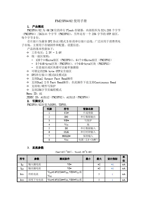
FM25C04
- 格式:pdf
- 大小:100.90 KB
- 文档页数:11
Conditions
/CS = VIL /CS = VCC VIN = 0 to VCC VOUT = GND to VCC
Min
Max
3 50
Units
mA µA µA µA V V V V MHz µs µs ns ns ns ns ns ns ns ns ns
-1 -1 -0.3 0.7 * VCC
Features
I Sequential read of entire array I 4 byte "Page write" mode to minimize total write time per byte I /WP pin and BLOCK WRITE protection to prevent inadvertent programming as well as programming ENABLE and DISABLE opcodes. I /HOLD pin to suspend data transfer I Typical 1µA standby current (ISB) for "L" devices and 0.1µA standby current for "LZ" devices. I Endurance: Up to 1,000,000 data changes I Data retention greater than 40 years
Parameter
Operating Current Standby Current Input Leakage Output Leakage CMOS Input Low Voltage CMOS Input High Voltage Output Low Voltage Output High Voltage SCK Frequency Input Rise Time Input Fall Time Clock High Time Clock Low Time Min /CS High Time /CS Setup Time Data Setup Time /HOLD Setup Time /CS Hold Time Data Hold Time /HOLD Hold Time Output Delay Output Hold Time /HOLD to Output Low Z Output Disable Time /HOLD to Output High Z Write Cycle Time
Temp. Range
Voltage Operating Range
2
FM25C040U Rev. B
FM25C040U 4K-Bit SPI Interface Serial CMOS EEPROM
Standard Voltage 4.5 ≤ VCC ≤ 5.5V Specifications Operating Conditions Absolute Maximum Ratings (Note 1)
High Voltage Generator and Program Timer
Decoder
EEPROM Array
Read/Write Amps
Data In/Out Register 8 Bits
Data Out Buffer
SO
Non-Volatile Status Register
SPI™ is a trademark of Motorola Corporation
Functions
I SPI MODE 0 interface I 4,096 bits organized as 512 x 8 I Extended 2.7V to 5.5V operating voltage I 2.1 MHz operation @ 4.5V - 5.5V I Self-timed programming cycle I "Programming complete" indicated by STATUS REGISTER polling I /WP pin and BLOCK WRITE protection
ns ns ns ns ns ms
Capacitance TA = 25°C, f = 2.1/1 MHz (Note 4)
Symbol
COUT CIN
AC Test Conditions
Output Load Input Pulse Levels Timing Measurement Reference Level CL = 200 pF 0.1 * VCC – 0.9 * VCC 0.3 * VCC - 0.7 * VCC
Ordering Information FM 25 C XX U LZ E XX
Package
Letter Description
N M8 MT8 None V E Blank L LZ Ultralite Density/Mode Interface 040 C 25 FM 8-pin DIP 8-pin SO 8-pin TSSOP 0 to 70°C -40 to +125°C -40 to +85°C 4.5V to 5.5V 2.7V to 5.5V 2.7V to 5.5V and <1µA Standby Current CS100UL Process 4K, mode 0 CMOS technology SPI Fairchild Nonvolatile Memory Prefix
Ambient Storage Temperature All Input or Output Voltage with Respect to Ground Lead Temp. (Soldering, 10 sec.) ESD Rating -65°C to +150°C +6.5V to -0.3V +300°C 2000V Ambient Operating Temperature FM25C040U FM25C040UE FM25C040UV Power Supply (VCC) 0°C to +70°C -40°C to +85°C -40°C to +125°C 4.5V to 5.5V
DC and AC Electrical Characteristics 4.5V ≤ VCC ≤ 5.5V (unless otherwise specified)
Symbol
ICC ICCSB IIL IOL VIL VIH VOL VOH fOP tRI tFI tCLH tCLL tCSH tCSS tDIS tHDS tCSN tDIN tHDN tPD tDH tLZ tDF tHZ tWP
Top View See Package Number N08E (N), M08A (M8), and MTC08 (MT8)
Pin Names
/CS SO /WP VSS SI SCK /HOLD VCC Chip Select Input Serial Data Output Write Protect Ground Serial Data Input Serial Clock Input Suspends Serial Data Power Supply
Block Diagram
/CS /HOLD SCK SI Instruction Register Instruction Decoder Control Logic and Clock Generators VCC VSS /WP
Address Counter/ Register
Program Enable VPP
FM25C040U 4K-Bit SPI Interface Serial CMOS EEPROM
February 2002
FM25C040U 4K-Bit SPI™ Interface Serial CMOS EEPROM
General Description
The FM25C040U is a 4K (4,096) bit serial interface CMOS EEPROM (Electrically Erasable Programmable Read-Only Memory). This device fully conforms to the SPI 4-wire protocol which uses Chip Select (/CS), Clock (SCK), Data-in (SI) and Dataout (SO) pins to synchronously control data transfer between the SPI microcontroller and the EEPROM. In addition, the serial interface allows a minimal pin count, packaging designed to simplify PC board layout requirements and offers the designer a variety of low voltage and low power options. This SPI EEPROM family is designed to work with the 68HC11 or any other SPI-compatible, high-speed microcontroller and offers both hardware (/WP pin) and software ("block write") data protection. For example, entering a 2-bit code into the STATUS REGISTER prevents programming in a selected block of memory and all programming can be inhibited by connecting the /WP pin to VSS; allowing the user to protect the entire array or a selected section. In addition, SPI devices feature a /HOLD pin, which allows a temporary interruption of the datastream into the EEPROM. Fairchild EEPROMs are designed and tested for applications requiring high endurance, high reliability, and low power consumption for a continuously reliable non-volatile solution for all markets.