外文资料翻译 --AT89S52单片机简介
- 格式:doc
- 大小:161.50 KB
- 文档页数:11

本科毕业设计(论文)AT89S52单片机应用中英文翻译专业名称:电气工程及其自动化年级班级:学生姓名:指导老师:二O一二年六月九日AT89S52 MCU ApplicationsFunction Characteristic DescriptionThe AT89S52 is a low-power, high-performance CMOS 8-bit microcontroller with 8K bytes of in-system programmable Flash memory. The device is manufactured using Atmel’s high-density nonvolatile memory technology and is compatible with the indus-try-standard 80C51 instruction set and pinout. The on-chip Flash allows the program memory to be reprogrammed in-system or by a conventional nonvolatile memory pro-grammer. By combining a versatile 8-bit CPU with in-system programmable Flash on a monolithic chip, the Atmel AT89S52 is a powerful microcontroller which provides a highly-flexible and cost-effective solution to many embedded control applications.The AT89S52 provides the following standard features: 8K bytes of Flash, 256 bytes of RAM, 32 I/O lines, Watchdog timer, two data pointers, three 16-bit timer/counters, a six-vector two-level interrupt architecture, a full duplex serial port, on-chip oscillator, and clock circuitry. In addition, the AT89S52 is designed with static logic for operation down to zero frequency and supports two software selectable power saving modes. The Idle Mode stops the CPU while allowing the RAM, timer/counters, serial port, and interrupt system to continue functioning. The Power-down mode saves the RAM con-tents but freezes the oscillator, disabling all other chip functions until the next interrupt or hardware reset.Pin DescriptionVCC :Supply voltage.GND :Ground.Port 0:Port 0 is an 8-bit open drain bidirectional I/O port. As an output port, each pin can sink eight TTL inputs. When 1s are written to port 0 pins, the pins can be used as high-impedance inputs. Port 0 can also be configured to be the multiplexed low-order address/data bus during accesses to external program and data memory. In this mode, P0 has internal pull-ups. Port 0 also receives the code bytes during Flash programming and outputs the code bytes dur-ing program verification. External pull-ups are required during program verification.Port 1:Port 1 is an 8-bit bidirectional I/O port with internal pull-ups. The Port 1 outputbuffers can sink/source four TTL inputs. When 1s are written to Port 1 pins, they are pulled high by the inter-nal pull-ups and can be used as inputs. As inputs, Port 1 pins that are externally being pulled low will source current (IIL) because of the internal pull-ups. In addition, P1.0 and P1.1 can be configured to be the timer/counter 2 external count input (P1.0/T2) and the timer/counter 2 trigger input (P1.1/T2EX), respectively, as shown in the follow-ing table 1. Port 1 also receives the low-order address bytes during Flash programming and verification.Port 2:Port 2 is an 8-bit bidirectional I/O port with internal pull-ups. The Port 2 output buffers can sink/source four TTL inputs. When 1s are written to Port 2 pins, they are pulled high by the inter-nal pull-ups and can be used as inputs. As inputs, Port 2 pins that are externally being pulled low will source current (IIL) because of the internal pull-ups. Port 2 emits the high-order address byte during fetches from external program memory and dur-ing accesses to external data memory that use 16-bit addresses (MOVX @ DPTR). In this application, Port 2 uses strong internal pull-ups when emitting 1s. During accesses to external data memory that use 8-bit addresses (MOVX @ RI), Port 2 emits the contents of the P2 Special Function Register. Port 2 also receives the high-order address bits and some control signals during Flash program-ming and verification.Port 3:Port 3 is an 8-bit bidirectional I/O port with internal pull-ups. The Port 3 output buffers can sink/source four TTL inputs. When 1s are written to Port 3 pins, they are pulled high by the inter-nal pull-ups and can be used as inputs. As inputs, Port 3 pins that areexternally being pulled low will source current (IIL) because of the pull-ups. Port 3 receives some control signals for Flash programming and verification. Port 3 also serves the functions of various special features of the AT89S52, as shown in the fol-lowing table 2.RST:Reset input. A high on this pin for two machine cycles while the oscillator is running resets the device. This pin drives high for 98 oscillator periods after the Watchdog times out. The DISRTO bit in SFR AUXR (address 8EH) can be used to disable this feature. In the default state of bit DISRTO, the RESET HIGH out feature is enabled.ALE/PROG:Address Latch Enable (ALE) is an output pulse for latching the low byte of the address during accesses to external memory. This pin is also the program pulse input (PROG) during Flash programming. In normal operation, ALE is emitted at a constant rate of 1/6 the oscillator frequency and may be used for external timing or clocking purposes. Note, however, that one ALE pulse is skipped dur-ing each access to external data memory. If desired, ALE operation can be disabled by setting bit 0 of SFR location 8EH. With the bit set, ALE is active only during a MOVX or MOVC instruction. Otherwise, the pin is weakly pulled high. Setting the ALE-disable bit has no effect if the microcontroller is in external execution mode.PSEN:Program Store Enable (PSEN) is the read strobe to external program memory. When the AT89S52 is executing code from external program memory, PSEN is activated twice each machine cycle, except that two PSEN activations are skipped during eachaccess to exter-nal data memory.EA/VPP:External Access Enable. EA must be strapped to GND in order to enable the device to fetch code from external program memory locations starting at 0000H up to FFFFH. Note, however, that if lock bit 1 is programmed, EA will be internally latched on reset. EA should be strapped to VCC for internal program executions. This pin also receives the 12-volt programming enable voltage (VPP) during Flash programming.XTAL1:Input to the inverting oscillator amplifier and input to the internal clock operating circuit.XTAL2:Output from the inverting oscillator amplifier.Program MemoryIf the EA pin is connected to GND, all program fetches are directed to external memory. On the AT89S52, if EA is connected to VCC, program fetches to addresses 0000H through 1FFFH are directed to internal memory and fetches to addresses 2000H through FFFFH are to external memory.Data MemoryThe AT89S52 implements 256 bytes of on-chip RAM. The upper 128 bytes occupy a parallel address space to the Special Function Registers. This means that the upper 128 bytes have the same addresses as the SFR space but are physically separate from SFR space. When an instruction accesses an internal location above address 7FH, the address mode used in the instruction specifies whether the CPU accesses the upper 128 bytes of RAM or the SFR space. Instructions which use direct addressing access the SFR space. For example, the following direct addressing instruction accesses the SFR at location 0A0H (which is P2). MOV 0A0H, #data. Instructions that use indirect addressing access the upper 128 bytes of RAM. For example, the following indirect addressing instruction, where R0 contains 0A0H, accesses the data byte at address 0A0H, rather than P2 (whose address is 0A0H).MOV @R0, #data. Note that stack operations are examples of indirect addressing, so the upper 128 bytes of data RAM are available as stack space.Watchdog TimerThe WDT is intended as a recovery method in situations where the CPU may be subjected to software upsets. The WDT consists of a 14-bit counter and the Watchdog Timer Reset (WDTRST) SFR. The WDT is defaulted to disable from exiting reset. To enable the WDT, a user must write 01EH and 0E1H in sequence to the WDTRST register (SFR location 0A6H). When the WDT is enabled, it will increment every machine cycle while the oscillator is running. The WDT timeout period is dependent on the external clock frequency. There is no way to disable the WDT except through reset (either hardware reset or WDT overflow reset). When WDT over-flows, it will drive an output RESET HIGH pulse at the RST pin.In Power-down mode the oscillator stops, which means the WDT also stops. While in Power-down mode, the user does not need to service the WDT. There are two methods of exiting Power-down mode: by a hardware reset or via a level-activated external interrupt which is enabled prior to entering Power-down mode. When Power-down is exited with hardware reset, servicing the WDT should occur as it normally does whenever the AT89S52 is reset. Exiting Power-down with an interrupt is significantly different. The interrupt is held low long enough for the oscillator to stabilize. When the interrupt is brought high, the interrupt is serviced. To prevent the WDT from resetting the device while the interrupt pin is held low, the WDT is not started until the interrupt is pulled high. It is suggested that the WDT be reset during the interrupt service for the interrupt used to exit Power-down mode. To ensure that the WDT does not overflow within a few states of exiting Power-down, it is best to reset the WDT just before entering Power-down mode. Before going into the IDLE mode, the WDIDLE bit in SFR AUXR is used to determine whether the WDT continues to count if enabled. The WDT keeps counting during IDLE (WDIDLE bit = 0) as the default state. To prevent the WDT from resetting the AT89S52 while in IDLE mode, the user should always set up a timer that will periodically exit IDLE, service the WDT, and reenter IDLE mode. With WDIDLE bit enabled, the WDT will stop to count in IDLE mode and resumes the count upon exit from IDLE.Timer 0 and 1Timer 0 and Timer 1 in the AT89S52 operate the same way as Timer 0 and Timer 1 in the AT89C51 and AT89C52. For further information o n the timers’ operation, please click on the document link below:/dyn/resources/prod_documents/DOC4316.PDFTimer 2Timer 2 is a 16-bit Timer/Counter that can operate as either a timer or an event counter. The type of operation is selected by bit C/T2in the SFR T2CON. Timer 2 has three operating modes: capture, auto-reload (up or down counting), and baud rate generator. The modes are selected by bits in T2CON, as shown in Table 6-1. Timer 2 consists of two 8-bit registers, TH2 and TL2. In the Timer function, the TL2 register is incremented every machine cycle. Since a machine cycle consists of 12 oscillator periods, the count rate is 1/12 of the oscil-lator frequency.In the Counter function, the register is incremented in response to a 1-to-0 transition at its corre-sponding external input pin, T2. In this function, the external input is sampled during S5P2 of every machine cycle. When the samples show a high in one cycle and a low in the next cycle, the count is incremented. The new count value appears in the register during S3P1 of the cycle following the one in which the transition was detected. Since two machine cycles (24 oscillator periods) are required to recognize a 1-to-0 transition, the maximum count rate is 1/24 of the oscillator frequency. To ensure that a given level is sampled at least once before it changes, the level should be held for at least one full machine cycle.InterruptsThe AT89S52 has a total of six interrupt vectors: two external interrupts (INT0and INT1), three timer interrupts (Timers 0, 1, and 2), and the serial port interrupt. Each of these interrupt sources can be individually enabled or disabled by setting or clearing a bit in Special Function Register IE. IE also contains a global disable bit, EA, which disables all interrupts at once. Note that bit position IE.6 is unimplemented. User software should not write a 1 to this bit position, since it may be used in future AT89 products. Timer 2 interrupt is generated by the logical OR of bits TF2 and EXF2 in register T2CON. Nei-ther of these flags is cleared by hardware when the service routine is vectored to. In fact, the service routine may have to determine whether it was TF2 or EXF2 that generated the interrupt, and that bit will have to be cleared in software. The Timer 0 and Timer 1 flags, TF0 and TF1, are set at S5P2 of the cycle in which the timers overflow. The values are then polled by the circuitry in the next cycle. However, the Timer 2 flag, TF2, is set at S2P2 and is polled in the same cycle in which the timer overflows.Oscillator CharacteristicsXTAL1 and XTAL2 are the input and output, respectively, of an inverting amplifier that can be configured for use as an on-chip oscillator. Either a quartz crystal or ceramic resonator may be used. To drive the device from an external clock source, XTAL2 should be left unconnected while XTAL1 is driven,. There are no requirements on the duty cycle of the external clock signal, since the input to the internal clock-ing circuitry is through a divide-by-two flip-flop, but minimum and maximum voltage high and low time specifications must be observed.Power-down ModeIn the Power-down mode, the oscillator is stopped, and the instruction that invokes Power-down is the last instruction executed. The on-chip RAM and Special Function Registers retain their values until the Power-down mode is terminated. Exit from Power-down mode can be initiated either by a hardware reset or by an enabled external interrupt. Reset redefines the SFRs but does not change the on-chip RAM. The reset should not be activated before VCC is restored to its normal operating level and must be heldactive long enough to allow the oscillator to restart and stabilize.Idle ModIn idle mode, the CPU puts itself to sleep while all the on-chip peripherals remain active. The mode is invoked by software. The content of the on-chip RAM and all the special functions regis-ters remain unchanged during this mode. The idle mode can be terminated by any enabled interrupt or by a hardware reset. Note that when idle mode is terminated by a hardware reset, the device normally resumes pro-gram execution from where it left off, up to two machine cycles before the internal reset algorithm takes control. On-chip hardware inhibits access to internal RAM in this event, but access to the port pins is not inhibited. To eliminate the possibility of an unexpected write to a port pin when idle mode is terminated by a reset, the instruction following the one that invokes idle mode should not write to a port pin or to external memory.AT89S52单片机应用功能特征描述AT89S52是一种低功耗、高性能CMOS8位微控制器,具有8K 在系统可编程Flash 存储器。

AT89S52简介AT89S52是一个8位单片机,片内ROM全部采用FLASH ROM技术,与MCS-51系列完全兼容,它能以3V的超低电压工作,晶振时钟最高可达24MHz。
AT89S52是标准的40引脚双列直插式集成电路芯片,有4个八位的并行双向I/O端口,分别记作P0、P1、P2、P3。
第31引脚需要接高电位使单片机选用内部程序存储器;第9引脚是复位引脚,要接一个上电手动复位电路;第40脚为电源端VCC,接+5V电源,第20引脚为接地端VSS,通常在VCC和VSS引脚之间接0.1μF高频滤波电容。
第18、19脚之间接上一个12MHz的晶振为单片机提供时钟信号。
AT89S52单片机说明如下:此芯片是一种高性能低功耗的采用CMOS工艺制造的8位微控制器,它提供下列标准特征:8K字节的程序存储器,256字节的RAM,32条I/O线,2个16位定时器/计数器, 一个5中断源两个优先级的中断结构,一个双工的串行口, 片上震荡器和时钟电路。
引脚说明::电源电压·VCC·GND:地·P0口:P0口是一组8位漏极开路型双向I/O口,作为输出口用时,每个引脚能驱动8个TTL逻辑门电路。
当对0端口写入1时,可以作为高阻抗输入端使用。
当P0口访问外部程序存储器或数据存储器时,它还可设定成地址数据总线复用的形式。
在这种模式下,P0口具有内部上拉电阻。
在EPROM编程时,P0口接收指令字节,同时输出指令字节在程序校验时。
程序校验时需要外接上拉电阻。
·P1口:P1口是一带有内部上拉电阻的8位双向I/O口。
P1口的输出缓冲能接受或输出4个TTL逻辑门电路。
当对P1口写1时,它们被内部的上拉电阻拉升为高电平,此时可以作为输入端使用。
当作为输入端使用时,P1口因为内)。
部存在上拉电阻,所以当外部被拉低时会输出一个低电流(IIL·P2口:P2是一带有内部上拉电阻的8位双向的I/O端口。
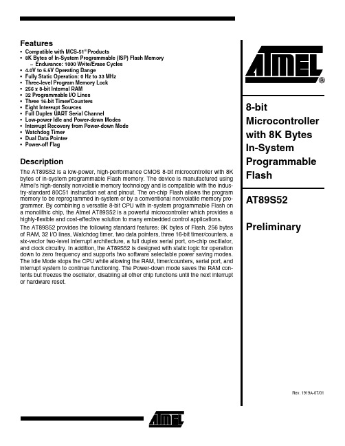
•Compatible with MCS-51® Products•8K Bytes of In-System Programmable (ISP) Flash Memory–Endurance: 1000 Write/Erase Cycles• 4.0V to 5.5V Operating Range•Fully Static Operation: 0 Hz to 33 MHz•Three-level Program Memory Lock•256 x 8-bit Internal RAM•32 Programmable I/O Lines•Three 16-bit Timer/Counters•Eight Interrupt Sources•Full Duplex UART Serial Channel•Low-power Idle and Power-down Modes•Interrupt Recovery from Power-down Mode•Watchdog Timer•Dual Data Pointer•Power-off FlagDescriptionThe AT89S52 is a low-power, high-performance CMOS 8-bit microcontroller with 8K bytes of in-system programmable Flash memory. The device is manufactured using Atmel’s high-density nonvolatile memory technology and is compatible with the indus-try-standard 80C51 instruction set and pinout. The on-chip Flash allows the program memory to be reprogrammed in-system or by a conventional nonvolatile memory pro-grammer. By combining a versatile 8-bit CPU with in-system programmable Flash on a monolithic chip, the Atmel AT89S52 is a powerful microcontroller which provides a highly-flexible and cost-effective solution to many embedded control applications. The AT89S52 provides the following standard features: 8K bytes of Flash, 256 bytes of RAM, 32 I/O lines, Watchdog timer, two data pointers, three 16-bit timer/counters, a six-vector two-level interrupt architecture, a full duplex serial port, on-chip oscillator, and clock circuitry. In addition, the AT89S52 is designed with static logic for operation down to zero frequency and supports two software selectable power saving modes. The Idle Mode stops the CPU while allowing the RAM, timer/counters, serial port, and interrupt system to continue functioning. The Power-down mode saves the RAM con-tents but freezes the oscillator, disabling all other chip functions until the next interruptor hardware reset.TQFPPLCCPin ConfigurationsPDIPAT89S52 Block DiagramPin DescriptionVCCSupply voltage.GNDGround.Port 0Port 0 is an 8-bit open drain bidirectional I/O port. As an output port, each pin can sink eight TTL inputs. When 1s are written to port 0 pins, the pins can be used as high-impedance inputs.Port 0 can also be configured to be the multiplexed low-order address/data bus during accesses to external program and data memory. In this mode, P0 has internal pullups.Port 0 also receives the code bytes during Flash program-ming and outputs the code bytes during program verifica-tion. External pullups are required during program verification.Port 1Port 1 is an 8-bit bidirectional I/O port with internal pullups. The Port 1 output buffers can sink/source four TTL inputs. When 1s are written to Port 1 pins, they are pulled high by the internal pullups and can be used as inputs. As inputs, Port 1 pins that are externally being pulled low will source current (I IL) because of the internal pullups.In addition, P1.0 and P1.1 can be configured to be the timer/counter 2 external count input (P1.0/T2) and the timer/counter 2 trigger input (P1.1/T2EX), respectively, as shown in the following table.Port 1 also receives the low-order address bytes during Flash programming and verification.Port 2Port 2 is an 8-bit bidirectional I/O port with internal pullups. The Port 2 output buffers can sink/source four TTL inputs. When 1s are written to Port 2 pins, they are pulled high by the internal pullups and can be used as inputs. As inputs, Port 2 pins that are externally being pulled low will source current (I IL) because of the internal pullups.Port 2 emits the high-order address byte during fetches from external program memory and during accesses to external data memory that use 16-bit addresses (MOVX @ DPTR). In this application, Port 2 uses strong internal pull-ups when emitting 1s. During accesses to external data memory that use 8-bit addresses (MOVX @ RI), Port 2 emits the contents of the P2 Special Function Register. Port 2 also receives the high-order address bits and some control signals during Flash programming and verification. Port 3Port 3 is an 8-bit bidirectional I/O port with internal pullups. The Port 3 output buffers can sink/source four TTL inputs. When 1s are written to Port 3 pins, they are pulled high by the internal pullups and can be used as inputs. As inputs, Port 3 pins that are externally being pulled low will source current (I IL) because of the pullups.Port 3 also serves the functions of various special features of the AT89S52, as shown in the following table.Port 3 also receives some control signals for Flash pro-gramming and verification.RSTReset input. A high on this pin for two machine cycles while the oscillator is running resets the device. This pin drives High for 96 oscillator periods after the Watchdog times out. The DISRTO bit in SFR AUXR (address 8EH) can be used to disable this feature. In the default state of bit DISRTO, the RESET HIGH out feature is enabled.ALE/PROGAddress Latch Enable (ALE) is an output pulse for latching the low byte of the address during accesses to external memory. This pin is also the program pulse input (PROG) during Flash programming.In normal operation, ALE is emitted at a constant rate of 1/6the oscillator frequency and may be used for external timing or clocking purposes. Note, however, that one ALE pulse is skipped during each access to external data memory.If desired, ALE operation can be disabled by setting bit 0 of SFR location 8EH. With the bit set, ALE is active only dur-ing a MOVX or MOVC instruction. Otherwise, the pin isPort Pin Alternate FunctionsP1.0T2 (external count input to Timer/Counter 2),clock-outP1.1T2EX (Timer/Counter 2 capture/reload triggerand direction control)P1.5MOSI (used for In-System Programming)P1.6MISO (used for In-System Programming)P1.7SCK (used for In-System Programming)Port Pin Alternate FunctionsP3.0RXD (serial input port)P3.1TXD (serial output port)P3.2INT0 (external interrupt 0)P3.3INT1 (external interrupt 1)P3.4T0 (timer 0 external input)P3.5T1 (timer 1 external input)P3.6WR (external data memory write strobe) P3.7RD (external data memory read strobe)AT89S52 weakly pulled high. Setting the ALE-disable bit has noeffect if the microcontroller is in external execution mode. PSENProgram Store Enable (PSEN) is the read strobe to exter-nal program memory.When the AT89S52 is executing code from external pro-cycle, except that two PSEN activations are skipped during each access to external data memory.EA/VPPExternal Access Enable. EA must be strapped to GND in order to enable the device to fetch code from external pro-gram memory locations starting at 0000H up to FFFFH.internally latched on reset.EA should be strapped to V CC for internal program execu-tions.This pin also receives the 12-volt programming enable volt-age (V PP) during Flash programming.XTAL1Input to the inverting oscillator amplifier and input to the internal clock operating circuit.XTAL2Output from the inverting oscillator amplifier.Table 1. AT89S52 SFR Map and Reset Values0F8H0FFH0F0HB000000000F7H0E8H0EFH0E0HACC000000000E7H0D8H0DFH0D0HPSW000000000D7H0C8HT2CON00000000T2MODXXXXXX00RCAP2L00000000RCAP2H00000000TL200000000TH2000000000CFH0C0H0C7H0B8HIPXX0000000BFH0B0HP3111111110B7H0A8HIE0X0000000AFH0A0HP211111111AUXR1XXXXXXX0WDTRSTXXXXXXXX0A7H98HSCON00000000SBUFXXXXXXXX9FH90HP11111111197H88HTCON00000000TMOD00000000TL000000000TL100000000TH000000000TH100000000AUXRXXX00XX08FH80HP011111111SP00000111DP0L00000000DP0H00000000DP1L00000000DP1H00000000PCON0XXX000087HSpecial Function RegistersA map of the on-chip memory area called the Special Func-tion Register (SFR) space is shown in Table 1.Note that not all of the addresses are occupied, and unoc-cupied addresses may not be implemented on the chip. Read accesses to these addresses will in general return random data, and write accesses will have an indetermi-nate effect.User software should not write 1s to these unlisted loca-tions, since they may be used in future products to invoke new features. In that case, the reset or inactive values of the new bits will always be 0.Timer 2 Registers: Control and status bits are contained in registers T2CON (shown in Table 2) and T2MOD (shown in Table 3) for Timer 2. The register pair (RCAP2H, RCAP2L) are the Capture/Reload registers for Timer 2 in 16-bit cap-ture mode or 16-bit auto-reload mode.Interrupt Registers: The individual interrupt enable bits are in the IE register. Two priorities can be set for each of the six interrupt sources in the IP register.Table 2. T2CON – Timer/Counter 2 Control RegisterT2CON Address = 0C8H Reset Value = 0000 0000BBit AddressableBit TF2EXF2RCLK TCLK EXEN2TR2C/T2CP/RL276543210Symbol FunctionTF2Timer 2 overflow flag set by a Timer 2 overflow and must be cleared by software. TF2 will not be set when either RCLK = 1 or TCLK = 1.EXF2Timer 2 external flag set when either a capture or reload is caused by a negative transition on T2EX and EXEN2 = 1.When Timer 2 interrupt is enabled, EXF2 = 1 will cause the CPU to vector to the Timer 2 interrupt routine. EXF2 must becleared by software. EXF2 does not cause an interrupt in up/down counter mode (DCEN = 1).RCLK Receive clock enable. When set, causes the serial port to use Timer 2 overflow pulses for its receive clock in serial port Modes 1 and 3. RCLK = 0 causes Timer 1 overflow to be used for the receive clock.TCLK Transmit clock enable. When set, causes the serial port to use Timer 2 overflow pulses for its transmit clock in serial port Modes 1 and 3. TCLK = 0 causes Timer 1 overflows to be used for the transmit clock.EXEN2Timer 2 external enable. When set, allows a capture or reload to occur as a result of a negative transition on T2EX if Timer2 is not being used to clock the serial port. EXEN2 = 0 causes Timer 2 to ignore events at T2EX.TR2Start/Stop control for Timer 2. TR2 = 1 starts the timer.C/T2Timer or counter select for Timer 2. C/T2 = 0 for timer function. C/T2 = 1 for external event counter (falling edge triggered). CP/RL2Capture/Reload select. CP/RL2 = 1 causes captures to occur on negative transitions at T2EX if EXEN2 = 1. CP/RL2 = 0 causes automatic reloads to occur when Timer 2 overflows or negative transitions occur at T2EX when EXEN2 = 1. When either RCLK or TCLK = 1, this bit is ignored and the timer is forced to auto-reload on Timer 2 overflow.AT89S52Dual Data Pointer Registers: To facilitate accessing both internal and external data memory, two banks of 16-bit Data Pointer Registers are provided: DP0 at SFR address locations 82H-83H and DP1 at 84H-85H. Bit DPS = 0 in SFR AUXR1 selects DP0 and DPS = 1 selects DP1. The user should always initialize the DPS bit to the appropriate value before accessing the respective Data Pointer Register.Power Off Flag: The Power Off Flag (POF) is located at bit 4 (PCON.4) in the PCON SFR. POF is set to “1” during power up. It can be set and rest under software control and is not affected by reset.Table 3a. AUXR: Auxiliary RegisterAUXR Address = 8EH Reset Value = XXX00XX0B Not Bit Addressable–––WDIDLE DISRTO––DISALE Bit76543210–Reserved for future expansionDISALE Disable/Enable ALEDISALE Operating Mode0ALE is emitted at a constant rate of 1/6 the oscillator frequency1ALE is active only during a MOVX or MOVC instructionDISRTO Disable/Enable Reset outDISRTO0Reset pin is driven High after WDT times out1Reset pin is input onlyWDIDLE Disable/Enable WDT in IDLE modeWDIDLE0WDT continues to count in IDLE mode1WDT halts counting in IDLE modeTable 3b. AUXR1: Auxiliary Register 1AUXR1Address = A2H Reset Value = XXXXXXX0B Not Bit Addressable–––––––DPS Bit76543210–Reserved for future expansionDPS Data Pointer Register SelectDPS0Selects DPTR Registers DP0L, DP0H1Selects DPTR Registers DP1L, DP1HMemory OrganizationMCS-51 devices have a separate address space for Pro-gram and Data Memory. Up to 64K bytes each of external Program and Data Memory can be addressed.Program Memorydirected to external memory.On the AT89S52, if EA is connected to V CC, program fetches to addresses 0000H through 1FFFH are directed to internal memory and fetches to addresses 2000H through FFFFH are to external memory.Data MemoryThe AT89S52 implements 256 bytes of on-chip RAM. The upper 128 bytes occupy a parallel address space to the Special Function Registers. This means that the upper 128 bytes have the same addresses as the SFR space but are physically separate from SFR space.When an instruction accesses an internal location above address 7FH, the address mode used in the instruction specifies whether the CPU accesses the upper 128 bytes of RAM or the SFR space. Instructions which use direct addressing access of the SFR space.For example, the following direct addressing instruction accesses the SFR at location 0A0H (which is P2).MOV0A0H,#dataInstructions that use indirect addressing access the upper 128 bytes of RAM. For example, the following indirect addressing instruction, where R0 contains 0A0H, accesses the data byte at address 0A0H, rather than P2 (whose address is 0A0H).MOV@R0,#dataNote that stack operations are examples of indirect addressing, so the upper 128 bytes of data RAM are avail-able as stack space.AT89S52Watchdog Timer(One-time Enabled with Reset-out)The WDT is intended as a recovery method in situations where the CPU may be subjected to software upsets. The WDT consists of a 13-bit counter and the Watchdog Timer Reset (WDTRST) SFR. The WDT is defaulted to disable from exiting reset. To enable the WDT, a user must write 01EH and 0E1H in sequence to the WDTRST register (SFR location 0A6H). When the WDT is enabled, it will increment every machine cycle while the oscillator is run-ning. The WDT timeout period is dependent on the external clock frequency. There is no way to disable the WDT except through reset (either hardware reset or WDT over-flow reset). When WDT overflows, it will drive an output RESET HIGH pulse at the RST pin.Using the WDTTo enable the WDT, a user must write 01EH and 0E1H in sequence to the WDTRST register (SFR location 0A6H). When the WDT is enabled, the user needs to service it by writing 01EH and 0E1H to WDTRST to avoid a WDT over-flow. The 13-bit counter overflows when it reaches 8191 (1FFFH), and this will reset the device. When the WDT is enabled, it will increment every machine cycle while the oscillator is running. This means the user must reset the WDT at least every 8191 machine cycles. To reset the WDT the user must write 01EH and 0E1H to WDTRST. WDTRST is a write-only register. The WDT counter cannot be read or written. When WDT overflows, it will generate an output RESET pulse at the RST pin. The RESET pulse duration is 96xTOSC, where TOSC=1/FOSC. To make the best use of the WDT, it should be serviced in those sec-tions of code that will periodically be executed within the time required to prevent a WDT reset.WDT During Power-down and IdleIn Power-down mode the oscillator stops, which means the WDT also stops. While in Power-down mode, the user does not need to service the WDT. There are two methods of exiting Power-down mode: by a hardware reset or via a level-activated external interrupt which is enabled prior to entering Power-down mode. When Power-down is exited with hardware reset, servicing the WDT should occur as it normally does whenever the AT89S52 is reset. Exiting Power-down with an interrupt is significantly different. The interrupt is held low long enough for the oscillator to stabi-lize. When the interrupt is brought high, the interrupt is serviced. To prevent the WDT from resetting the device while the interrupt pin is held low, the WDT is not started until the interrupt is pulled high. It is suggested that the WDT be reset during the interrupt service for the interrupt used to exit Power-down mode.To ensure that the WDT does not overflow within a few states of exiting Power-down, it is best to reset the WDT just before entering Power-down mode.Before going into the IDLE mode, the WDIDLE bit in SFR AUXR is used to determine whether the WDT continues to count if enabled. The WDT keeps counting during IDLE (WDIDLE bit = 0) as the default state. To prevent the WDT from resetting the AT89S52 while in IDLE mode, the user should always set up a timer that will periodically exit IDLE, service the WDT, and reenter IDLE mode.With WDIDLE bit enabled, the WDT will stop to count in IDLE mode and resumes the count upon exit from IDLE.UARTThe UART in the AT89S52 operates the same way as the UART in the AT89C51 and AT89C52. For further informa-tion on the UART operation, refer to the ATMEL Web site (). From the home page, select ‘Prod-ucts’, then ‘8051-Architecture Flash Microcontroller’, then ‘Product Overview’.Timer 0 and 1Timer 0 and Timer 1 in the AT89S52 operate the same way as Timer 0 and Timer 1 in the AT89C51 and AT89C52. For further information on the timers’ operation, refer to the ATMEL Web site (). From the home page, select ‘Products’, then ‘8051-Architecture Flash Microcontroller’, then ‘Product Overview’.Timer 2Timer 2 is a 16-bit Timer/Counter that can operate as either a timer or an event counter. The type of operation is Timer 2 has three operating modes: capture, auto-reload (up or down counting), and baud rate generator. The modes are selected by bits in T2CON, as shown in Table 3. Timer 2 consists of two 8-bit registers, TH2 and TL2. In the Timer function, the TL2 register is incremented every machine cycle. Since a machine cycle consists of 12 oscil-lator periods, the count rate is 1/12 of the oscillator frequency.Table 3. Timer 2 Operating ModesRCLK +TCLK CP/RL2TR2MODE00116-bit Auto-reload01116-bit Capture1X1Baud Rate GeneratorX X0(Off)In the Counter function, the register is incremented in response to a 1-to-0 transition at its corresponding external input pin, T2. In this function, the external input is sampled during S5P2 of every machine cycle. When the samples show a high in one cycle and a low in the next cycle, the count is incremented. The new count value appears in the register during S3P1 of the cycle following the one in which the transition was detected. Since two machine cycles (24 oscillator periods) are required to recognize a 1-to-0 transi-tion, the maximum count rate is 1/24 of the oscillator fre-quency. To ensure that a given level is sampled at least once before it changes, the level should be held for at least one full machine cycle.Capture ModeIn the capture mode, two options are selected by bit EXEN2 in T2CON. If EXEN2 = 0, Timer 2 is a 16-bit timer or counter which upon overflow sets bit TF2 in T2CON.This bit can then be used to generate an interrupt. If EXEN2 = 1, Timer 2 performs the same operation, but a 1-to-0 transition at external input T2EX also causes the current value in TH2 and TL2 to be captured into RCAP2H and RCAP2L, respectively. In addition, the transition at T2EX causes bit EXF2 in T2CON to be set. The EXF2 bit, like TF2, can generate an interrupt. The capture mode is illustrated in Figure 5.Auto-reload (Up or Down Counter)Timer 2 can be programmed to count up or down when configured in its 16-bit auto-reload mode. This feature is invoked by the DCEN (Down Counter Enable) bit located in the SFR T2MOD (see Table 4). Upon reset, the DCEN bit is set to 0 so that timer 2 will default to count up. When DCEN is set, Timer 2 can count up or down, depending on the value of the T2EX pin.Figure 5. Timer in Capture ModeFigure 6 shows Timer 2 automatically counting up when DCEN=0. In this mode, two options are selected by bit EXEN2 in T2CON. If EXEN2 = 0, Timer 2 counts up to 0FFFFH and then sets the TF2 bit upon overflow. The overflow also causes the timer registers to be reloaded with the 16-bit value in RCAP2H and RCAP2L. The values in Timer in Capture ModeRCAP2H and RCAP2L are preset by software. If EXEN2 = 1, a 16-bit reload can be triggered either by an overflow or by a 1-to-0 transition at external input T2EX. This transition also sets the EXF2 bit. Both the TF2 and EXF2 bits can generate an interrupt if enabled. Setting the DCEN bit enables Timer 2 to count up or down, as shown in Figure 6. In this mode, the T2EX pin controls the direction of the count. A logic 1 at T2EX makes Timer 2 count up. The timer will overflow at 0FFFFH and set the TF2 bit. This overflow also causes the 16-bit value in RCAP2H and RCAP2L to be reloaded into the timer regis-ters, TH2 and TL2, respectively.A logic 0 at T2EX makes Timer 2 count down. The timer underflows when TH2 and TL2 equal the values stored in RCAP2H and RCAP2L. The underflow sets the TF2 bit and causes 0FFFFH to be reloaded into the timer registers. The EXF2 bit toggles whenever Timer 2 overflows or underflows and can be used as a 17th bit of resolution. In this operating mode, EXF2 does not flag an interrupt.AT89S52 Figure 6. Timer 2 Auto Reload Mode (DCEN = 0)Table 4. T2MOD – Timer 2 Mode Control RegisterT2MOD Address = 0C9H Reset Value = XXXX XX00B Not Bit Addressable––––––T2OE DCEN Bit76543210Symbol Function–Not implemented, reserved for futureT2OE Timer 2 Output Enable bitDCEN When set, this bit allows Timer 2 to be configured as an up/down counterFigure 7. Timer 2 Auto Reload Mode (DCEN = 1)Figure 8. Timer 2 in Baud Rate Generator ModeAT89S52Baud Rate GeneratorTimer 2 is selected as the baud rate generator by setting TCLK and/or RCLK in T2CON (Table 2). Note that the baud rates for transmit and receive can be different if Timer 2 is used for the receiver or transmitter and Timer 1 is used for the other function. Setting RCLK and/or TCLK puts Timer 2 into its baud rate generator mode, as shown in Fig-ure 8.The baud rate generator mode is similar to the auto-reload mode, in that a rollover in TH2 causes the Timer 2 registers to be reloaded with the 16-bit value in registers RCAP2H and RCAP2L, which are preset by software.The baud rates in Modes 1 and 3 are determined by Timer 2’s overflow rate according to the following equation.The Timer can be configured for either timer or counteroperation. In most applications, it is configured for timer Timer 2 when it is used as a baud rate generator. Normally,as a timer, it increments every machine cycle (at 1/12 the oscillator frequency). As a baud rate generator, however, itincrements every state time (at 1/2 the oscillator fre-quency). The baud rate formula is given below.where (RCAP2H, RCAP2L) is the content of RCAP2H and RCAP2L taken as a 16-bit unsigned integer.Timer 2 as a baud rate generator is shown in Figure 8. This figure is valid only if RCLK or TCLK = 1 in T2CON. Note that a rollover in TH2 does not set TF2 and will not gener-ate an interrupt. Note too, that if EXEN2 is set, a 1-to-0transition in T2EX will set EXF2 but will not cause a reload from (RCAP2H, RCAP2L) to (TH2, TL2). Thus, when Timer 2 is in use as a baud rate generator, T2EX can be used as an extra external interrupt.Note that when Timer 2 is running (TR2 = 1) as a timer in the baud rate generator mode, TH2 or TL2 should not be read from or written to. Under these conditions, the Timer is incremented every state time, and the results of a read or write may not be accurate. The RCAP2 registers may be read but should not be written to, because a write might overlap a reload and cause write and/or reload errors. The timer should be turned off (clear TR2) before accessing the Timer 2 or RCAP2 registers.Figure 9. Timer 2 in Clock-Out ModeModes 1 and 3 Baud Rates Timer 2 Overflow Rate16-----------------------------------------------------------=Modes 1 and 3Baud Rate ---------------------------------------Oscillator Frequency 32 x [65536-RCAP2H,RCAP2L)]-------------------------------------------------------------------------------------=Programmable Clock OutA 50% duty cycle clock can be programmed to come out on P1.0, as shown in Figure 9. This pin, besides being a regu-lar I/O pin, has two alternate functions. It can be pro-grammed to input the external clock for Timer/Counter 2 or to output a 50% duty cycle clock ranging from 61 Hz to 4MHz at a 16 MHz operating frequency.To configure the Timer/Counter 2 as a clock generator, bit must be set. Bit TR2 (T2CON.2) starts and stops the timer.The clock-out frequency depends on the oscillator fre-quency and the reload value of Timer 2 capture registers (RCAP2H, RCAP2L), as shown in the following equation.In the clock-out mode, Timer 2 roll-overs will not generate an interrupt. This behavior is similar to when Timer 2 is used as a baud-rate generator. It is possible to use Timer 2as a baud-rate generator and a clock generator simulta-neously. Note, however, that the baud-rate and clock-out frequencies cannot be determined independently from one another since they both use RCAP2H and RCAP2L.InterruptsThe AT89S52 has a total of six interrupt vectors: two exter-ers 0, 1, and 2), and the serial port interrupt. These interrupts are all shown in Figure 10.Each of these interrupt sources can be individually enabled or disabled by setting or clearing a bit in Special Function Register IE. IE also contains a global disable bit, EA, which disables all interrupts at once.Note that Table 5 shows that bit position IE.6 is unimple-mented. In the AT89S52, bit position IE.5 is also unimple-mented. User software should not write 1s to these bit positions, since they may be used in future AT89 products.Timer 2 interrupt is generated by the logical OR of bits TF2and EXF2 in register T2CON. Neither of these flags is cleared by hardware when the service routine is vectored to. In fact, the service routine may have to determine whether it was TF2 or EXF2 that generated the interrupt,and that bit will have to be cleared in software.The Timer 0 and Timer 1 flags, TF0 and TF1, are set at S5P2 of the cycle in which the timers overflow. The values are then polled by the circuitry in the next cycle. However,the Timer 2 flag, TF2, is set at S2P2 and is polled in the same cycle in which the timer overflows.Table 5. Interrupt Enable (IE) RegisterFigure 10. Interrupt SourcesClock-Out Frequency Oscillator Frequency4 x [65536-(RCAP2H,RCAP2L)]------------------------------------------------------------------------------------= (MSB) (LSB)EA–ET2ESET1EX1ET0EX0Enable Bit = 1 enables the interrupt. Enable Bit = 0 disables the interrupt.Symbol Position FunctionEAIE.7Disables all interrupts. If EA =0, no interrupt is acknowledged. If EA = 1, each interrupt source is individually enabled or disabled by setting or clearing its enable bit.–IE.6Reserved.ET2IE.5Timer 2 interrupt enable bit.ES IE.4Serial Port interrupt enable bit.ET1IE.3Timer 1 interrupt enable bit.EX1IE.2External interrupt 1 enable bit.ET0IE.1Timer 0 interrupt enable bit.EX0IE.0External interrupt 0 enable bit.User software should never write 1s to unimplemented bits, because they may be used in future AT89 products.AT89S52Oscillator CharacteristicsXTAL1 and XTAL2 are the input and output, respectively, of an inverting amplifier that can be configured for use as an on-chip oscillator, as shown in Figure 11. Either a quartz crystal or ceramic resonator may be used. To drive the device from an external clock source, XTAL2 should be left unconnected while XTAL1 is driven, as shown in Figure 12. There are no requirements on the duty cycle of the external clock signal, since the input to the internal clocking circuitry is through a divide-by-two flip-flop, but minimum and maxi-mum voltage high and low time specifications must be observed.Idle ModeIn idle mode, the CPU puts itself to sleep while all the on-chip peripherals remain active. The mode is invoked by software. The content of the on-chip RAM and all the spe-cial functions registers remain unchanged during this mode. The idle mode can be terminated by any enabled interrupt or by a hardware reset.Note that when idle mode is terminated by a hardware reset, the device normally resumes program execution from where it left off, up to two machine cycles before the internal reset algorithm takes control. On-chip hardware inhibits access to internal RAM in this event, but access to the port pins is not inhibited. To eliminate the possibility of an unexpected write to a port pin when idle mode is termi-nated by a reset, the instruction following the one that invokes idle mode should not write to a port pin or to exter-nal memory.Power-down ModeIn the Power-down mode, the oscillator is stopped, and the instruction that invokes Power-down is the last instruction executed. The on-chip RAM and Special Function Regis-ters retain their values until the Power-down mode is termi-nated. Exit from Power-down mode can be initiated either by a hardware reset or by an enabled external interrupt. Reset redefines the SFRs but does not change the on-chip RAM. The reset should not be activated before V CC is restored to its normal operating level and must be held active long enough to allow the oscillator to restart and stabilize.Figure 11. Oscillator ConnectionsNote: C1, C2 = 30 pF ± 10 pF for Crystals= 40 pF ± 10 pF for Ceramic Resonators Figure 12. External Clock Drive ConfigurationTable 6. Status of External Pins During Idle and Power-down ModesMode Program Memory ALE PSEN PORT0PORT1PORT2PORT3 Idle Internal11Data Data Data Data Idle External11Float Data Address Data Power-down Internal00Data Data Data Data Power-down External00Float Data Data Data。

(文档含英文原文和中文翻译)中英文资料对照外文翻译英文原文:The Description of MCUMCU DescriptionSCM is also known as micro-controller (Microcontroller Unit), commonly used letters of the acronym MCU MCU that it was first used in industrial control. Only a single chip by the CPU chip developed from a dedicated processor. The first design is by a large number of peripherals and CPU on a chip in the computer system, smaller, more easily integrated into a complex and demanding on the volume control device which. INTEL's Z80 is the first designed in accordance with this idea processor, then on the development of microcontroller and dedicated processors have parted ways.Are 8-bit microcontroller early or 4 bits. One of the most successful is the INTEL 8031, for a simple, reliable and good performance was a lot of praise. Then developed in 8031 out of MCS51 MCU Systems. SCM systems based on this system until now is still widely used. With the increased requirements of industrial control field, began a 16-bit microcontroller, because the cost is not satisfactory but have not been very widely used. After 90 years with the great development of consumer electronics, microcontroller technology has been a huge increase. With INTEL i960 series, especially the later series of widely used ARM, 32-bit microcontroller quickly replace high-end 16-bit MCU status and enter the mainstream market. The traditional 8-bit microcontroller performance have been the rapid increase capacity increase compared to 80 the number of times. Currently, high-end 32-bit microcontroller clocked over 300MHz, the performance catching the mid-90's dedicated processor, while the average model prices fall to one U.S. dollars, the most high-end [1] model only 10 dollars. Modern SCM systems are no longer only in the development and use of bare metal environment, a large number of proprietary embedded operating system is widely used in the full range of SCM. The handheld computers and cell phones as the core processing of high-end microcontroller can even use a dedicated Windows and Linux operating systems.SCM is more suitable than the specific processor used in embedded systems, so it was up to the application. In fact the number of SCM is the world's largest computer. Modern human life used in almost every piece of electronic and mechanical products will be integrated single chip. Phone, telephone, calculator, home appliances, electronic toys, handheld computers and computer accessories such as a mouse with a 1-2 in both the Department of SCM. Personal computer will have a large number of SCM in the work. General car with more than 40 SCM, complex industrial control systems may even have hundreds of SCM in the same time work! SCM is not only far exceeds the number of PC and other computing the sum, or even more than the number of human beingsSingle chip, also known as single-chip microcontroller, it is not complete a certain logic chips, but to a computer system integrated into a chip. Equivalent to a micro-computer, and computer than just the lack of a microcontroller I / O devices. General talk: a chip becomes a computer. Its small size, light weight, cheap, for the study, application and development of facilities provided. At the same time, learning to use the MCU is to understand the principle and structure of the computer the best choice.SCM and the computer functions internally with similar modules, such as CPU, memory, parallel bus, the same effect as well, and hard disk memory devices, and different is its performance of these components were relatively weak many of our home computer, but the price is low , usually not more than 10 yuan you can do with it ...... some control for a class is not very complicated electrical work is enough of. We are using automatic drum washing machine, smoke hood, VCD and so on appliances which could see its shadow! ...... It is primarily as a control section of the core componentsIt is an online real-time control computer, control-line is that the scene is needed is a stronger anti-jamming ability, low cost, and this is, and off-line computer (such as home PC), the main difference.Single chipMCU is through running, and can be modified. Through different procedures to achieve different functions, in particular special unique features, this is another device much effort needs to be done, some great efforts are very difficult to do. A not very complex functions if the 50's with the United States developed 74 series, or the 60's CD4000 series of these pure hardware buttoned, then the circuit must be a large PCB board! But if the United States if the 70's with a series of successful SCM market, the result will be a drastic change! Just because you are prepared by microcomputer programs can achieve high intelligence, high efficiency and high reliability!As the microcontroller on the cost-sensitive, so now the dominant software or the lowest level assembly language, which is the lowest level in addition to more than binary machine code language, and as so low why is the use? Many high-level language has reached the level of visual programming Why is not it? The reason is simply that there is no home computer as a single chip CPU, not as hard as a mass storage device. A visualization of small high-level language program which even if only one button, will reach tens of K of size! For the home PC's hard drive in terms of nothing, but in terms of the MCU is not acceptable. SCM in the utilization of hardware resources to be very high for the job so although the original is still in the compilation of a lot of use. The same token, if the giant computer operating system and applications run up to get home PC, home PC, also can not afford to.Can be said that the twentieth century across the three "power" era, that is, the age of electricity, the electronic age and has entered into the computer age. However, this computer, usually refers to the personal computer, referred to as PC. It consists of thehost, keyboard, monitor and other components. Another type of computer, most people do not know how. This computer is to give all kinds of intelligent machines single chip (also known as micro-controller). As the name suggests, this computer system took only a minimal integrated circuit, can be a simple operation and control. Because it is small, usually hidden in the charged mechanical "stomach" in. It is in the device, like the human brain plays a role, it goes wrong, the whole plant was paralyzed. Now, this microcontroller has a very broad field of use, such as smart meters, real-time industrial control, communications equipment, navigation systems, and household appliances. Once all kinds of products were using SCM, can serve to upgrade the effectiveness of products, often in the product name preceded by the adjective - "intelligent," such as intelligent washing machines. Now some technical personnel of factories or other amateur electronics developers to engage in out of certain products, not the circuit is too complicated, that function is too simple and can easily be copied. The reason may be stuck in the product did not use a microcontroller or other programmable logic device.SCM historySCM was born in the late 20th century, 70, experienced SCM, MCU, SoC three stages.First model1.SCM the single chip microcomputer (Single Chip Microcomputer) stage, mainly seeking the best of the best single form of embedded systems architecture. "Innovation model" success, laying the SCM and general computer completely different path of development. In the open road of independent development of embedded systems, Intel Corporation contributed.2.MCU the micro-controller (Micro Controller Unit) stage, the main direction of technology development: expanding to meet the embedded applications, the target system requirements for the various peripheral circuits and interface circuits, highlight the object of intelligent control. It involves the areas associated with the object system, therefore, the development of MCU's responsibility inevitably falls on electrical, electronics manufacturers. From this point of view, Intel faded MCU development has its objective factors. In the development of MCU, the most famous manufacturers as the number of Philips Corporation.Philips company in embedded applications, its great advantage, the MCS-51 single-chip micro-computer from the rapid development of the micro-controller. Therefore, when we look back at the path of development of embedded systems, do notforget Intel and Philips in History.Embedded SystemsEmbedded system microcontroller is an independent development path, the MCU important factor in the development stage, is seeking applications to maximize the solution on the chip; Therefore, the development of dedicated single chip SoC trend of the natural form. As the microelectronics, IC design, EDA tools development, application system based on MCU SoC design have greater development. Therefore, the understanding of the microcontroller chip microcomputer can be, extended to the single-chip micro-controller applications.MCU applicationsSCM now permeate all areas of our lives, which is almost difficult to find traces of the field without SCM. Missile navigation equipment, aircraft, all types of instrument control, computer network communications and data transmission, industrial automation, real-time process control and data processing, extensive use of various smart IC card, civilian luxury car security system, video recorder, camera, fully automatic washing machine control, and program-controlled toys, electronic pet, etc., which are inseparable from the microcontroller. Not to mention the area of robot control, intelligent instruments, medical equipment was. Therefore, the MCU learning, development and application of the large number of computer applications and intelligent control of the scientists, engineers.The single-chip microcomputer AT89S52 MCU as an example, the pair for further description:AT89S52 MCUFeatures• Compatible with MCS-51 Products• 8K Bytes of In-System Programmable (ISP) Flash Memory – Endurance: 10,000 Write/Erase Cycles• 4.0V to 5.5V Operating Range• Fully Static Operation: 0 Hz to 33 MHz• Three-level Program Memory Lock• 256 x 8-bit Internal RAM• 32 Programmable I/O Lines• Three 16-bit Timer/Counters• Eight Interrupt Sources• Full Duplex UART Serial Channel• Low-power Idle and Power-down Modes• Interrupt Recov ery from Power-down Mode• Watchdog Timer • Dual Data Pointer• Power-off Flag • Fast Programming Time• Flexible ISP Programming (Byte and Page Mode)• Green (Pb/Halide-free) Packaging Option1.DescriptionThe AT89S52 is a low-power, high-performance CMOS 8-bit microcontroller with 8K bytes of in-system programmable Flash memory. The device is manufactured using Atmel’s high-density nonvolatile memory technology and is compatible with the indus-try-standard 80C51 instruction set and pinout. The on-chip Flash allows the program memory to be reprogrammed in-system or by a conventional nonvolatile memory pro-grammer. By combining a versatile 8-bit CPU with in-system programmable Flash on a monolithic chip, the Atmel AT89S52 is a powerful microcontroller which provides a highly-flexible and cost-effective solution to many embedded control applications.The AT89S52 provides the following standard features: 8K bytes of Flash, 256 bytes of RAM, 32 I/O lines, Watchdog timer, two data pointers, three 16-bit timer/counters, a six-vector two-level interrupt architecture, a full duplex serial port, on-chip oscillator, and clock circuitry. In addition, the AT89S52 is designed with static logic for operation down to zero frequency and supports two software selectable power saving modes. The Idle Mode stops the CPU while allowing the RAM, timer/counters, serial port, and interrupt system to continue functioning. The Power-down mode saves the RAM con-tents but freezes the oscillator, disabling all other chip functions until the next interrupt or hardware reset.2.Pin DescriptionVCC :Supply voltage.GND :Ground.Port 0:Port 0 is an 8-bit open drain bidirectional I/O port. As an output port, eachpin can sink eight TTL inputs. When 1s are written to port 0 pins, the pins can be used as high-impedance inputs. Port 0 can also be configured to be the multiplexed low-order address/data bus during accesses to external program and data memory. In this mode, P0 has internal pull-ups. Port 0 also receives the code bytes during Flash programming and outputs the code bytes dur-ing program verification. External pull-ups are required during program verification.Port 1:Port 1 is an 8-bit bidirectional I/O port with internal pull-ups. The Port 1 output buffers can sink/source four TTL inputs. When 1s are written to Port 1 pins, they are pulled high by the inter-nal pull-ups and can be used as inputs. As inputs, Port 1 pins that are externally being pulled low will source current (IIL) because of the internal pull-ups. In addition, P1.0 and P1.1 can be configured to be the timer/counter 2 external count input (P1.0/T2) and the timer/counter 2 trigger input (P1.1/T2EX), respectively, as shown in the follow-ing table.Port 1 also receives the low-order address bytes during Flash programming and verification.Port 2:Port 2 is an 8-bit bidirectional I/O port with internal pull-ups. The Port 2 output buffers can sink/source four TTL inputs. When 1s are written to Port 2 pins, they are pulled high by the inter-nal pull-ups and can be used as inputs. As inputs, Port 2 pins that are externally being pulled low will source current (IIL) because of the internal pull-ups. Port 2 emits the high-order address byte during fetches from external program memory and dur-ing accesses to external data memory that use 16-bit addresses (MOVX @ DPTR). In this application, Port 2 uses strong internal pull-ups when emitting 1s. During accesses to external data memory that use 8-bit addresses (MOVX@ RI), Port 2 emits the contents of the P2 Special Function Register. Port 2 also receives the high-order address bits and some control signals during Flash program-ming and verification.Port 3:Port 3 is an 8-bit bidirectional I/O port with internal pull-ups. The Port 3 output buffers can sink/source four TTL inputs. When 1s are written to Port 3 pins, they are pulled high by the inter-nal pull-ups and can be used as inputs. As inputs, Port 3 pins that are externally being pulled low will source current (IIL) because of the pull-ups. Port 3 receives some control signals for Flash programming and verification. Port 3 also serves the functions of various special features of the AT89S52, as shown in the fol-lowing table.RST:Reset input. A high on this pin for two machine cycles while the oscillator is running resets the device. This pin drives high for 98 oscillator periods after the Watchdog times out. The DISRTO bit in SFR AUXR (address 8EH) can be used to disable this feature. In the default state of bit DISRTO, the RESET HIGH out feature is enabled.ALE/PROG:Address Latch Enable (ALE) is an output pulse for latching the low byte of the address during accesses to external memory. This pin is also the program pulse input (PROG) during Flash programming. In normal operation, ALE is emitted at a constant rate of 1/6 the oscillator frequency and may be used for external timing orclocking purposes. Note, however, that one ALE pulse is skipped dur-ing each access to external data memory. If desired, ALE operation can be disabled by setting bit 0 of SFR location 8EH. With the bit set, ALE is active only during a MOVX or MOVC instruction. Otherwise, the pin is weakly pulled high. Setting the ALE-disable bit has no effect if the microcontroller is in external execution mode.PSEN:Program Store Enable (PSEN) is the read strobe to external program memory. When the AT89S52 is executing code from external program memory, PSEN is activated twice each machine cycle, except that two PSEN activations are skipped during each access to exter-nal data memory.EA/VPP:External Access Enable. EA must be strapped to GND in order to enable the device to fetch code from external program memory locations starting at 0000H up to FFFFH. Note, however, that if lock bit 1 is programmed, EA will be internally latched on reset. EA should be strapped to VCC for internal program executions. This pin also receives the 12-volt programming enable voltage (VPP) during Flash programming.XTAL1:Input to the inverting oscillator amplifier and input to the internal clock operating circuit.XTAL2:Output from the inverting oscillator amplifier.3.Memory OrganizationMCS-51 devices have a separate address space for Program and Data Memory. Up to 64K bytes each of external Program and Data Memory can be addressed.3.1 Program MemoryIf the EA pin is connected to GND, all program fetches are directed to external memory. On the AT89S52, if EA is connected to VCC, program fetches to addresses 0000H through 1FFFH are directed to internal memory and fetches to addresses 2000H through FFFFH are to external memory.3.2 Data MemoryThe AT89S52 implements 256 bytes of on-chip RAM. The upper 128 bytes occupy a parallel address space to the Special Function Registers. This means that the upper 128 bytes have the same addresses as the SFR space but are physically separate from SFR space. When an instruction accesses an internal location above address 7FH, the address mode used in the instruction specifies whether the CPU accesses the upper 128bytes of RAM or the SFR space. Instructions which use direct addressing access the SFR space. For example, the following direct addressing instruction accesses the SFR at location 0A0H (which is P2).MOV 0A0H, #dataInstructions that use indirect addressing access the upper 128 bytes of RAM. For example, the following indirect addressing instruction, where R0 contains 0A0H, accesses the data byte at address 0A0H, rather than P2 (whose address is 0A0H).MOV @R0, #dataNote that stack operations are examples of indirect addressing, so the upper 128 bytes of data RAM are available as stack space.4.Watchdog Timer (One-time Enabled with Reset-out)The WDT is intended as a recovery method in situations where the CPU may be subjected to software upsets. The WDT consists of a 14-bit counter and the Watchdog Timer Reset (WDTRST) SFR. The WDT is defaulted to disable from exiting reset. To enable the WDT, a user must write 01EH and 0E1H in sequence to the WDTRST register (SFR location 0A6H). When the WDT is enabled, it will increment every machine cycle while the oscillator is running. The WDT timeout period is dependent on the external clock frequency. There is no way to disable the WDT except through reset (either hardware reset or WDT overflow reset). When WDT over-flows, it will drive an output RESET HIGH pulse at the RST pin.4.1 Using the WDTTo enable the WDT, a user must write 01EH and 0E1H in sequence to the WDTRST register (SFR location 0A6H). When the WDT is enabled, the user needs to service it by writing 01EH and 0E1H to WDTRST to avoid a WDT overflow. The 14-bit counter overflows when it reaches 16383 (3FFFH), and this will reset the device. When the WDT is enabled, it will increment every machine cycle while the oscillator is running. This means the user must reset the WDT at least every 16383 machine cycles. To reset the WDT the user must write 01EH and 0E1H to WDTRST. WDTRST is a write-only register. The WDT counter cannot be read or written. When WDT overflows, it will generate an output RESET pulse at the RST pin. The RESET pulse dura-tion is 98xTOSC, where TOSC = 1/FOSC. To make the best use of the WDT, it should be serviced in those sections of code that will periodically be executed within the time required to prevent a WDT reset.4.2 WDT During Power-down and IdleIn Power-down mode the oscillator stops, which means the WDT also stops. While in Power-down mode, the user does not need to service the WDT. There are two methods of exiting Power-down mode: by a hardware reset or via a level-activated external interrupt which is enabled prior to entering Power-down mode. When Power-down is exited with hardware reset, servicing the WDT should occur as it normally does whenever the AT89S52 is reset. Exiting Power-down with an interrupt is significantly different. The interrupt is held low long enough for the oscillator to stabilize. When the interrupt is brought high, the interrupt is serviced. To prevent the WDT from resetting the device while the interrupt pin is held low, the WDT is not started until the interrupt is pulled high. It is suggested that the WDT be reset during the interrupt service for the interrupt used to exit Power-down mode. To ensure that the WDT does not overflow within a few states of exiting Power-down, it is best to reset the WDT just before entering Power-down mode. Before going into the IDLE mode, the WDIDLE bit in SFR AUXR is used to determine whether the WDT continues to count if enabled. The WDT keeps counting during IDLE (WDIDLE bit = 0) as the default state. To prevent the WDT from resetting the AT89S52 while in IDLE mode, the user should always set up a timer that will periodically exit IDLE, service the WDT, and reenter IDLE mode. With WDIDLE bit enabled, the WDT will stop to count in IDLE mode and resumes the count upon exit from IDLE.5. UARTThe UART in the AT89S52 operates the same way as the UART in the AT89C51 and AT89C52. For further information on the UART operation, please click on the document link below:/dyn/resources/prod_documents/DOC4316.PDF6. Timer 0 and 1Timer 0 and Timer 1 in the AT89S52 operate the same way as Timer 0 and Timer 1 in the AT89C51 and AT89C52. For further information on the timers’ operation, please click on the document link below:/dyn/resources/prod_documents/DOC4316.PDF7. Timer 2Timer 2 is a 16-bit Timer/Counter that can operate as either a timer or an event counter. The type of operation is selected by bit C/T2in the SFR T2CON. Timer 2 has three operating modes: capture, auto-reload (up or down counting), and baud rate generator. The modes are selected by bits in T2CON, as shown in Table 6-1. Timer 2 consists of two 8-bit registers, TH2 and TL2. In the Timer function, the TL2 register is incremented every machine cycle. Since a machine cycle consists of 12 oscillator periods, the count rate is 1/12 of the oscil-lator frequency.In the Counter function, the register is incremented in response to a 1-to-0 transition at its corre-sponding external input pin, T2. In this function, the external input is sampled during S5P2 of every machine cycle. When the samples show a high in one cycle and a low in the next cycle, the count is incremented. The new count value appears in the register during S3P1 of the cycle following the one in which the transition was detected. Since two machine cycles (24 oscillator periods) are required to recognize a 1-to-0 transition, the maximum count rate is 1/24 of the oscillator frequency. To ensure that a given level is sampled at least once before it changes, the level should be held for at least one full machine cycle.7.1 Capture ModeIn the capture mode, two options are selected by bit EXEN2 in T2CON. If EXEN2 = 0, Timer 2 is a 16-bit timer or counter which upon overflow sets bit TF2 in T2CON. This bit can then be used to generate an interrupt. If EXEN2 = 1, Timer 2 performs the same operation, but a 1-to-0 transi-tion at external input T2EX also causes the current value in TH2 and TL2 to be captured into RCAP2H and RCAP2L, respectively. In addition, the transition at T2EX causes bit EXF2 in T2CON to be set. The EXF2 bit, like TF2, can generate an interrupt.7.2 Auto-reload (Up or Down Counter)Timer 2 can be programmed to count up or down when configured in its 16-bit auto-reload mode. This feature is invoked by the DCEN (Down Counter Enable) bit located in the SFR T2MOD . Upon reset, the DCEN bit is set to 0 so that timer 2 will default to count up. When DCEN is set, Timer 2 can count up or down, depending on the value of the T2EX pin. Timer 2 automatically counting up when DCEN = 0. In this mode, two options are selected by bit EXEN2 in T2CON. If EXEN2 = 0, Timer 2 counts up to 0FFFFH and then sets the TF2 bit upon overflow. The overflow also causes the timer registers to be reloaded with the 16-bit value in RCAP2H and RCAP2L. The values in Timer in Capture ModeRCAP2H and RCAP2L are preset by software. If EXEN2 = 1, a 16-bit reload can be triggered either by an overflow or by a 1-to-0 transition at external input T2EX. This transition also sets the EXF2 bit. Both the TF2 and EXF2 bits can generate an interrupt if enabled. Setting the DCEN bit enables Timer 2 to count up or down, as shown in Figure 10-2. In this mode, the T2EX pin controls the direction of the count. A logic 1 at T2EX makes Timer 2 count up. The timer will overflow at 0FFFFH and set the TF2 bit. This overflow also causes the 16-bit value in RCAP2H and RCAP2L to be reloaded into the timer registers, TH2 and TL2, respectively. A logic 0 at T2EX makes Timer 2 count down. The timer underflows when TH2 and TL2 equal the values stored in RCAP2H and RCAP2L. The underflow sets the TF2 bit and causes 0FFFFH to be reloaded into the timer registers. The EXF2 bit toggles whenever Timer 2 overflows or underflows and can be used as a 17th bit of resolution. In this operating mode, EXF2 does not flag an interrupt.8. Baud Rate GeneratorTimer 2 is selected as the baud rate generator by setting TCLK and/or RCLK in T2CON. Note that the baud rates for transmit and receive can be different if Timer 2 is used for the receiver or transmitter and Timer 1 is used for the other function. Setting RCLK and/or TCLK puts Timer 2 into its baud rate generator mode. The baud rate generator mode is similar to the auto-reload mode, in that a rollover in TH2 causes the Timer 2 registers to be reloaded with the 16-bit value in registers RCAP2H and RCAP2L, which are preset by software. The baud rates in Modes 1 and 3 are determined by Timer 2’s overflow rate according to the fol -lowing equation.The Timer can be configured for either timer or counter operation. In most applications, it is con-figured for timer operation (CP/T2 = 0). The timer operation is Timer 2 Overflow Rate Modes 1 and 3 Baud Rates = 16different for Timer 2 when it is used as a baud rate generator. Normally, as a timer, it increments every machine cycle (at 1/12 the oscillator frequency). As a baud rate generator, however, it increments every state time (at 1/2 the oscillator frequency). The baud rate formula is given below.where (RCAP2H, RCAP2L) is the content of RCAP2H and RCAP2L taken as a 16-bit unsigned integer.This figure is valid only if RCLK or TCLK = 1 in T2CON. Note that a rollover in TH2 does not set TF2 and will not generate an inter-rupt. Note too, that if EXEN2 is set, a 1-to-0 transition in T2EX will set EXF2 but will not cause a reload from (RCAP2H, RCAP2L) to (TH2, TL2). Thus, when Timer 2 is in use as a baud rate generator, T2EX can be used as an extra external interrupt. Note that when Timer 2 is running (TR2 = 1) as a timer in the baud rate generator mode, TH2 or TL2 should not be read from or written to. Under these conditions, the Timer is incremented every state time, and the results of a read or write may not be accurate. The RCAP2 registers may be read but should not be written to, because a write might overlap a reload and cause write and/or reload errors. The timer should be turned off (clear TR2) before accessing the Timer 2 or RCAP2 registers.9. Programmable Clock OutA 50% duty cycle clock can be programmed to come out on P1.0. This pin, besides being a regular I/O pin, has two alternate functions. It can be programmed to input the external clock for Timer/Counter 2 or to output a 50% duty cycle clock ranging from 61 Hz to 4 MHz (for a 16-MHz operating frequency). To configure the Timer/Counter 2 as a clock generator, bit C/T2 (T2CON.1) must be cleared and bit T2OE (T2MOD.1) must be set. Bit TR2 (T2CON.2) starts and stops the timer. The clock-out frequency depends on the oscillator frequency and the reload value of Timer 2 capture registers (RCAP2H, RCAP2L), as shown in the following equation.In the clock-out mode, Timer 2 roll-overs will not generate an interrupt. This behavior is similar to when Timer 2 is used as a baud-rate generator. It is possible to use Timer 2 as a baud-rate gen-erator and a clock generator simultaneously. Note, however, Modes 1 and 3Oscillator Frequency Baud Rate 32[65536-RCAP2H,RCAP2L]=⨯Oscilator Frequency Clock-Out Frequency=4[65536-(RCAP2H,RCAP2L)]⨯。

外文翻译--AT89C52单片机的介绍外文翻译AT89C52 单片机的介绍AT89C52 单片机是一款广泛应用于各种电子设备中的微控制器。
它具有高性能、低功耗、易于编程等优点,为许多电子项目的实现提供了强大的支持。
AT89C52 单片机拥有丰富的内部资源。
它包含 8KB 的可重复编程的 Flash 存储器,用于存储程序代码。
这使得开发者可以方便地修改和更新程序,而无需更换硬件。
此外,它还有 256 字节的内部 RAM,用于数据的临时存储和处理。
在处理能力方面,AT89C52 单片机采用了 8 位的中央处理器(CPU),工作频率可达 24MHz。
虽然相比于现代的高性能处理器,它的处理速度不算快,但对于许多简单的控制任务和实时性要求不高的应用来说,已经足够胜任。
例如,在一些小型的家电控制、简单的测量仪器以及玩具等产品中,AT89C52 单片机能够准确、稳定地执行控制逻辑。
该单片机的引脚功能也十分丰富。
它通常具有 40 个引脚,包括电源引脚、时钟引脚、复位引脚以及多个输入输出引脚。
电源引脚用于提供单片机正常工作所需的电压,一般为 5V。
时钟引脚则连接外部晶振,为单片机提供工作时钟。
复位引脚用于系统的初始化和异常情况下的恢复。
而众多的输入输出引脚可以配置为不同的工作模式,如输入模式用于接收外部信号,输出模式用于控制外部设备。
在编程方面,AT89C52 单片机支持多种编程语言,如汇编语言和 C 语言。
汇编语言虽然编写较为复杂,但执行效率高;C 语言则更易于理解和编写,适合较大规模的程序开发。
通过专门的编程工具,如Keil C51 等,可以将编写好的程序下载到单片机中,实现特定的功能。
AT89C52 单片机在通信方面也具备一定的能力。
它可以通过串行通信接口(UART)与其他设备进行数据交换。
这种通信方式在与计算机、传感器、显示屏等外部设备连接时非常有用。
例如,在数据采集系统中,单片机可以通过 UART 接口将采集到的数据发送给计算机进行进一步处理和分析。

外文原文AT89S52DescriptionThe AT89s52 is a low-power, high-performance CMOS 8-bit microcomputer with 8K bytes of Flash programmable and erasable read only memory(PEROM). The device is manufactured using Atmel’s high-density nonvolatile memory technology and is compatible with the industry-standard 80C51 and 80C52 instruction set and pinout. The on-chip Flash allows the program memory to be reprogrammed in-system or by a conventional nonvolatile memory programmer. By combining a versatile 8-bit CPU with Flash on a monolithic chip, the Atmel AT89s52 is a powerful microcomputer which provides a highly-flexible and cost-effective solution to many embedded control applications.Pin Configurations: The AT89s52 provides the following standard features: 8K bytes of Flash, 256 bytes of RAM, 32 I/O lines, three 16-bittimer/counters, a six-vector two-level interrupt architecture, a full-duplex serial port, on-chip oscillator, and clock circuitry. In addition, the AT89s52 is designed with static logic for operation down to zero frequency and supports two software selectable power saving modes. The Idle Mode stops the CPU while allowing the RAM, timer/counters, serial port, and interrupt system to continue functioning. The Power-down mode saves the RAM contents but freezes the oscillator, disabling all other chip functions until the next hardware reset.Pin Description·VCC: Supply voltage.·GND: Ground.·Port 0: Port 0 is an 8-bit open drain bi-directional I/O port. As an output port, each pin can sink eight TTL inputs. When 1s are written to port 0 pins, the pins can be used as highimpedance inputs.Port 0 can also be configured to be the multiplexed loworder address/data bus during accesses to external program and data memory. In this mode, P0 has internalpullups.Port 0 also receives the code bytes during Flash programming and outputs the code bytes during program verification. External pullups are required during program verification.·Port 1: Port 1 is an 8-bit bi-directional I/O port with internal pullups. The Port 1 output buffers can sink/source four TTL inputs. When 1s are written to Port 1 pins, they are pulled high by the internal pullups and can be used as inputs. As inputs, Port 1 pins)because of the internal that are externally being pulled low will source current (IILpullups.In addition, P1.0 and P1.1 can be configured to be the timer/counter 2 external count input(P1.0/T2) and the timer/counter 2 trigger input (P1.1/T2EX), respectively, as shown in the following table.Port 1 also receives the low-order address bytes during Flash programming and verification.Port Pin Alternate FunctionP1.0 T2(external count input to Timer/Counter2),clock-outP1.1 T2EX(Time/Counter2 capture/reload triggerand direction control)·Port 2: Port 2 is an 8-bit bi-directional I/O port with internal pullups. The Port 2 output buffers can sink/source four TTL inputs. When 1s are written to Port 2 pins, they are pulled high by the internal pullups and can be used as inputs. As inputs, Port 2 pins)because of the internal that are externally being pulled low will source current (IILpullups.Port 2 emits the high-order address byte during fetches from external program memory and during accesses to external data memory that use 16-bit addresses (MOVX @DPTR). In this application, Port 2 uses strong internal pullups when emitting 1s. During accesses to external data memory that use 8-bit addresses (MOVX @ RI), Port 2 emits the contents of the P2 Special Function Register.Port 2 also receives the high-order address bits and some control signals duringFlash programming and verification.·Port 3: Port 3 is an 8-bit bi-directional I/O port with internal pullups. The Port 3 output buffers can sink/source four TTL inputs. When 1s are written to Port 3 pins, they are pulled high by the internal pullups and can be used as inputs. As inputs, Port 3 pins that are externally being pulled low will source current (I) because of the pullups.ILPort 3 also serves the functions of various special features of the AT89C51, as shown in the following table.Port 3 also receives some control signals for Flash programming and verification.Port Pin Alternate FunctionP3.0 RXD (serial input port)P3.1 TXD(serial output port)P3.2 external interrupt 0P3.3 external interrupt 1P3.4 T0(timer 0 external input)P3.5 T1(timer 1 external input)P3.6 external data memory write strobeP3.7 external data memory read strobe ·RST: Reset input. A high on this pin for two machine cycles while the oscillator is running resets the device.·ALE/PROG: Address Latch Enable is an output pulse for latching the low byte of the address during accesses to external memory. This pin is also the program pulse input (PROG) during Flash programming.In normal operation, ALE is emitted at a constant rate of 1/6 the oscillator frequency and may be used for external timing or clocking purposes. Note, however, that one ALE pulse is skipped during each access to external data memory.If desired, ALE operation can be disabled by setting bit 0 of SFR location 8EH. With the bit set, ALE is active only during a MOVX or MOVC instruction. Otherwise, the pin is weakly pulled high. Setting the ALE-disable bit has no effect if the microcontroller is in external execution mode.·PSEN: Program Store Enable is the read strobe to external program memory.When the AT89s52 is executing code from external program memory, PSEN is activated twice each machine cycle, except that two PSEN activations are skipped during each access to external data memory.·EA/VPP: External Access Enable. EA must be strapped to GND in order to enable the device to fetch code from external program memory locations starting at 0000H up to FFFFH.Note, however, that if lock bit 1 is programmed, EA will be internally latched on reset.EA should be strapped to V CC for internal program executions.This pin also receives the 12-volt programming enable voltage (V PP) during Flash programming when 12-volt programming is selected.·XTAL1I: nput to the inverting oscillator amplifier and input to the internal clock operating circuit.·XTAL2: Output from the inverting oscillator amplifier.Oscillator Characteristics: XTAL1 and XTAL2 are the input and output, respectively, of an inverting amplifier which can be configured for use as an on-chip oscillator, as shown in Figure 1. Either a quartz crystal or ceramic resonator may be used. To drive the device from an external clock source, XTAL2 should be left unconnected while XTAL1 is driven as shown in Figure 2. There are no requirements on the duty cycle of the external clock signal, since the input to the internal clocking circuitry is through a divide-by-two flip-flop, but minimum and maximum voltage high and low time specifications must be observed.Idle Mode: In idle mode, the CPU puts itself to sleep while all the onchip peripherals remain active. The mode is invoked by software. The content of the on-chip RAM and all the special functions registers remain unchanged during this mode. The idle mode can be terminated by any enabled interrupt or by a hardware reset.It should be noted that when idle is terminated by a hard ware reset, the device normally resumes program execution, from where it left off, up to two machine cycles before the internal reset algorithm takes control. On-chip hardware inhibits access tointernal RAM in this event, but access to the port pins is not inhibited. To eliminate the possibility of an unexpected write to a port pin when Idle is terminated by reset, the instruction following the one that invokes Idle should not be one that writes to a port pin or to external memory.Status of External Pins During Idle and Power Down Modes:Power Down Mode: In the power down mode the oscillator is stopped, and the instruction that invokes power down is the last instruction executed. The on-chip RAM and Special Function Registers retain their values until the power down mode is terminated. The only exit from power down is a hardware reset. Reset redefines the SFRs but does not change the on-chip RAM. The reset should not be activated before VCC is restored to its normal operating level and must be held active long enough to allow the oscillator to restart and stabilize.Program Memory Lock Bits: On the chip are three lock bits which can be left unprogrammed (U) or can be programmed (P) to obtain the additional features listed in the table below:Lock Bit Protection ModesWhen lock bit 1 is programmed, the logic level at the EA pin is sampled and latched during reset. If the device is powered up without a reset, the latch initializes to a random value, and holds that value until reset is activated. It is necessary that the latched value of EA be in agreement with the current logic level at that pin in order for the device to function properly.Programming the Flash: The at89s52 is normally shipped with the on-chip Flash memory array in the erased state (that is, contents = FFH) and ready to be programmed. The programming interface accepts either a high-voltage (12-volt) or a low-voltage(VCC) program enable signal.The low voltage programming mode provides a convenient way to program the at89s52 inside the user’s system, while the high-voltage programming mode is compatible with conventional third party Flash or EPROM programmers.The at89s52 is shipped with either the high-voltage or low-voltage programming mode enabled. The respective top-side marking and device signature codes are listed in the following table.The at89s52 code memory array is programmed byte-bybyte in either programming mode. To program any nonblank byte in the on-chip Flash Programmable and Erasable Read Only Memory, the entire memory must be erased using the Chip Erase Mode.Programming Algorithm: Before programming the at89s52, the address, data and control signals should be set up according to the Flash programming mode table and Figures 3 and 4. To program the at89s52, take the following steps.1. Input the desired memory location on the address lines.2. Input the appropriate data byte on the data lines.3. Activate the correct combination of control signals.4. Raise EA/VPP to 12V for the high-voltage programming mode.5. Pulse ALE/PROG once to program a byte in the Flash array or the lock bits. The byte-write cycle is self-timed and typically takes no more than 1.5 ms. Repeat steps 1 through 5, changing the address and data for the entire array or until the end of the object file is reached.Data Polling: The at89s52 features Data Polling to indicate the end of a write cycle. During a write cycle, an attempted read of the last byte written will result in the complement of the written datum on PO.7. Once the write cycle has been completed, true data are valid on all outputs, and the next cycle may begin. Data Polling may begin any time after a write cycle has been initiated.Ready/Busy: The progress of byte programming can also be monitored by the RDY/BSY output signal. P3.4 is pulled low after ALE goes high during programming to indicate BUSY. P3.4 is pulled high again when programming is done to indicate READY.Program Verify: If lock bits LB1 and LB2 have not been programmed, the programmed code data can be read back via the address and data lines for verification. The lock bits cannot be verified directly. Verification of the lock bits is achieved by observing that their features are enabled.Chip Erase:The entire Flash Programmable and Erasable Read Only Memory array is erased electrically by using the proper combination of control signals and by holding ALE/PROG low for 10 ms. The code array is written with all “1”s. The chip erase operation must be executed before the code memory can be re-programmed.Reading the Signature Bytes: The signature bytes are read by the same procedure as a normal verification of locations 030H, 031H, and 032H, except that P3.6 and P3.7 must be pulled to a logic low. The values returned are as follows.(030H) = 1EH indicates manufactured by Atmel(031H) = 51H indicates 89C51(032H) = FFH indicates 12V programming(032H) = 05H indicates 5V programmingProgramming Interface: Every code byte in the Flash array can be written and the entire array can be erased by using the appropriate combination of control signals. The write operation cycle is selftimed and once initiated, will automatically time itself to completion.中文翻译AT89S52AT89s52是美国ATMEL公司生产的低功耗,高性能COMS 8位单片机,片内含8K bytes的可反复擦写的Flash只读程序存储器和256 bytes的随机存取数据存储器(RAM),器件采用ATMEL公司的高密度、非易是失性存储技术生产,与标准MCS-51指令系统及8052产品引脚兼容,片内置通用8位中央处理器(CPU)和Flash存储单元,功能强大AT89s52单片机适用许多较为复杂控制应用场合。
中文4800字附录3:外文翻译AT89C52 monolithic integrated circuit introduction AT89C52 is the low voltage which American ATMEL Corporation produces, the high performance CMOS 8 monolithic integrated circuits, internal may repeatedly scratch read-only program memory (PEROM) and 256bytes random access data-carrier storage (RAM) including 8k bytes which writes, the component uses ATMEL Corporation the high density, the non-volatility memory technology production, is compatible with the standard MCS-51 command system and 8052 product pins, internal sets at general 8 central processor (CPU) and the Flash memory cell, the function formidable AT89C52 monolithic integrated circuit suits in many comparatively plurality of controls application situation.Main performance parameter:Are completely compatible with the MCS-51 product instruction and the pinThe 8k byte may again scratch writes Flash to dodge the fast memory1000 times scratches the write cycleEntire static operation: 0Hz—24MHzThree level of encryption program memory256×8 In byte RAM32 programmable I/O mouth line3 16 fixed time/counters8 interrupt sourcesProgrammable serial UART channelThe low power loss idle and falls the electricity patternFunction characteristic outline:Below AT89C52 provides the standard function: 8k byte Flash dodges the fast memory, 256 byte internal RAM,32 I/O mouth line, 3 16 fixed time/counters, 6 vector two level of interrupt structures, A full-duplex serial passes unguardedly, internal oscillator and clock electric circuit.At the same time, AT89C52 may fall to the 0HZ static state logical operation, and supports the electricity saving working pattern which two kind of softwares may elect.The idle way stops CPU the work, but permits RAM, fixed time/the counter, serial passes unguardedly and the interruption system continues to work.Falls the electricity way to preserve in RAM the content, but the oscillator knock off and forbids other all part work to reposition until the next hardware.The pin function showsVcc: Supply voltageGND: GroundingP0 mouth: The P0 mouth is one group of 8 leaks leads the way extremely the bidirectional I/O mouth, also is the address/data bus multiplying mouth.As outlet with when, each potential energy absorption current way actuates 8 TTL logic gate, when writes “1” to port P0, may take the high impedance input end uses.When visits exterior data-carrier storage or the program memory, when this group of mouth line segment transforms the address (low 8) and the data bus multiplying, pulls the resistance in the visit activation interior.When Flash programming, P0 mouth receive instruction byte, but when program check, when output order byte, verification, outside the request joins pulls the resistanceP1 mouth: P1 is in a belt interior pulls the resistance 8 bidirectional I/O mouth, the P1 output buffer may actuate (absorption or output current) 4 TTL logic gate.Writes “1” to the port, pulls the resistance through internal on to pull the port tothe high level, this time may make the input port.When makes the input port use, because in internal existence pulls the resistance, some pin is pulled lowly by exterior signal when can output electric current (IIL).With at89C51 similarity is, P1.0 and P1.1 also may take separately fixed time/the counter 2 exterior countings inputs (P1.0/T2) and inputs (P1.1/T2EX), see also table 1.Flash programming and program check period, P1 receives the low 8 bit address.P2 mouth: P2 is one has in the interior to pull the resistance 8 bidirectional I/O mouth, the P2 output buffer may actuate (absorption or output current) 4 TTL logic gate.Writes “1” to port P2, pulls the resistance through internal on to pull the port to the high level, this time may make the input port, when makes the input port use, because in internal existence pulls the resistance, some pin is pulled lowly by exterior signal when can output electric current (IIL).When visits exterior program memory or 16 bit address exterior data-carrier storage (e.g. carries out the MOVX@DPTR instruction), the P2 mouth sends out the high 8 bit address data.When visits 8 bit addresses exterior data-carrier storage (for example carries out the MOVX@RI instruction), the P2 mouth outputs the P2 latch the contentWhen Flash programming or verification, P2 also receives the top digit address and some control signal.P3 mouth: The P3 mouth is a group has in the interior to pull the resistance 8 bidirectional I/O mouth.The P3 mouth output buffer may actuate (absorption or output current) 4 TTL logic gate.Reads in “1” when to the P3 mouth, they the position resistance are pulled by the interior in Gao Bingke the achievement to input the port.This time, will be pulled by the outside the low P3 mouth to use to pull resistance output current (IIL).The P3 mouth besides took the general I/O mouth line, a more important use isIn addition, the P3 mouth also receives some to use in Flash dodging the fast memory programming and the program check control signal.RST: Replacement input.When the oscillator works, the RST pin will appear above two machine cycles the high level to cause the monolithic replacement.ALE/PROG: When visits exterior program memory or the data-carrier storage, ALE (address lock saves permission) to output the pulse to use in the lock saving the address the low 8 bytes.In ordinary circumstances, ALE still by clock oscilation frequency 1/6 output fixed pulse signal, therefore it may the foreign output clock or uses in fixed time the goal.Must pay attention: When visits exterior data-carrier storage will jump over a ALE pulse.To Flash memory programming period, this pin also uses in inputting programming pulse (PROG).If has the necessity, may through to in special function register (SFR) area 8EH the unit D0 position position, be possible to forbid the ALE operation.After this position position, only then MOVX and the MOVC instruction can activate ALE.In addition, this pin can pull weakly high, when the monolithic integrated circuit carries out exterior procedure, should establish the ALE prohibition position to be invalid PSEN: The procedure storage permits the (PSEN) output is exterior program memory reads the gating signal, when AT89C52 takes the instruction by exterior program memory (or data), each machine cycle two PSEN is effective, namely outputs two pulses.When visits exterior data-carrier storage, will jump over two RSEN signals.EA/VPP: Exterior visit permission.Wants to cause CPU only to visit exterior program memory (address is 0000H-FFFFH), the EA end must maintain the low level (earth).Must pay attention: If adds mil LB1 to program, when replacement the interiorcan lock saves the EA end condition.If the EA end (meets the Vcc end) for the high level, CPU carries out in the internal procedure memory instruction.When the Flash memory programs, this pin adds on 12V programming permission power source VPP, certainly this must be this component is uses 12V to program voltage VPP.XTAL1: Oscillator inverting amplifier and internal clock generator input end.XTAL2: Oscillator inverting amplifier out-port. Special function register:In at89C52 internal memory, the 80H-FFH altogether 128 units for special function register (SFE), SFR address basement reflection as shown in Table 2.All addresses all are defined by no means, only then a part is defined from the 80H-FFH altogether 128 bytes, but also has quite a part not to define.To the definition unit read-write will not have been Yuan Xiao, the read-out value will be indefinite, but will read in the data will also lose.Should not “1” not read in the data the definition unit, then will possibly entrust with the new function in these units in the future product, in this case, after replacement these unit value always “0”.AT89C52 besides with AT89C51 all fixed time/counters 0 and fixed time/counter 1, but also increased a fixed time/counter 2.Fixed time/the counter 2 control statusbyte is located T2CON、T2MOD (to see Table 4), the register to (RCA02H, RCAP2L) is the timer 2/automatic loads the register again under 16 capture ways or 16 automatic heavy loading way capture.Interrupt register:AT89C52 has 6 interrupt sources, 2 interrupt priorities, the IE register controls each interrupt position, in the IP register 6 interrupt source each may decide as 2 superiordata-carrier storages:AT89C52 has 256 byte internal RAM,80H-FFH high 128 bytes and the special function register (SFR) address is overlap, also is high 128 byte RAM and the special function register address is same, but in physics they are separated.When an instruction visits the 7FH above dummy home address unit, in the instruction uses the addressing way is different, also is the addressing way decision is visits high 128 byte RAM to visit the special function register.If the instruction is the direct addressing way for the visit special function register.For example, following direct addressing instruction visit special function register 0A0H (i.e. P2 mouth) address unit.MOV 0A0H,#dataThe indirect addressing instruction visits high 128 byte RAM, for example, in following indirect addressing instruction, the R0 content is 0A0H, then the visit data byte address is 0A0H, but is not the P2 mouth (0A0H).MOV the @R0,#datastorehouse operation also is the indirect addressing way, therefore, high 128 bit data RAM also may take the storehouse area use.Timer 0 and timer 1:The AT89C52 timer 0 and the timer 1 working and AT89C51 are same.Timer 2:The timer 2 is 16 fixed time/counters.It already may when timer use, also may take the external event counter use, its working chooses by the special function register T2CON C/T2 position.The timer 2 has three workings: The capture way, the automatic heavy loading (upward or downward counting) the way and the baudrate generator way, the working chooses by the T2CON control position, see also table 4.The timer 2 is composed by two 8 register TH2 and TL2, in the timer working, each machine cycle TL2 register value adds 1, because a machine cycle vibrates the clock constitution by 12, therefore, counting speed for oscilation frequency 1/12.When counting working, when on the T2 pin exterior input signal produces by 1 to 0 drops along, the register value adds 1, under this working, each machine cycle 5SP2 period, carries on the sampling to exterior input. If picks in the first machine cycle the value is 1, but the value which picks in the next machine cycle is 0, then is following close on the next cyclical S3P1 period register adds 1.Because distinguishes 1 to need 2 machine cycles to 0 jumps (24 durations of oscillation), therefore, highest counting speed for oscilation frequency 1/24. In order to guarantee the sampling the accuracy, the request input level maintains at least before the change for a complete cyclical the time, guarantees the input signal at least by sampling one time.Capture way:Under the capture way, chooses two ways through T2CON control position EXEN2.If EXEN2=0, the timer 2 is 16 timers or the counter, when counting overflow, to the T2CON overflow symbolized TF2 sets at the position, simultaneously activates the interrupt.If looks up EXEN2=1, the timer 2 completes the same operation, But when the T2EX pin exterior input signal has 1 to 0 negative jumps, also appears in TH2 and the TL2 value is caught separately to in RCAP2H and RCAP2L.Moreover, the T2EX pin signal jump causes in T2CON EXF2 to set at the position, is similar with TF2, EXF2 also can interrupt exactly.Capture way as shown in Figure 4.Automatic heavy loading (upward or downward counter) way:When timer 2 work in 16 automatic heavy loading ways, can to its programming for upward or the downward counting way, this function may (see Table 5) through special function register T2CON the DCEN position (permission downward counting) choose.When replacement, the DCEN position “0”, the timer 2 defaults establishes as the upward counting. When DCEN sets at the position, the timer 2 already may count upwardly also may the downward counting, this is decided by the T2EX pin value,see also Figure 5, when DCEN=0, the timer 2 automatic setups for the upward counting, under this way, in the T2CON EXEN2 control position have two kind of choices, if EXEN2=0, the timer 2 for the upward counting to the 0FFFFH overflow, sets at the position TF2 activation interrupt, simultaneously 16 counter register RCAP2H and the RCAP2L heavy loading, RCAP2H and the RCAP2L value may by the software initialization.When DCEN sets at the position, the timer 2 already may count upwardly also may the downward counting, this is decided by the T2EX pin value, see also Figure 5, when DCEN=0, the timer 2 automatic setups for the upward counting, under this way, in the T2CON EXEN2 control position have two kind of choices, if EXEN2=0, the timer 2 for the upward counting to the 0FFFFH overflow, sets at the position TF2 activation interrupt, simultaneously 16 counter register RCAP2H and the RCAP2L heavy loading, RCAP2H and the RCAP2L value may by the software initialization.Baudrate generator:When T2CON (Table 3) TCLK and RCLK set at the position, fixed time/the counter 2 takes the baudrate generator use.If fixed time/the counter 2 took thetransmitter or the receiver, its transmission and the receive baudrate may be different, the timer 1 uses in other functions, as shown in Figure 7.If RCLK and TCLK set at the position, then timer 2 work in baudrate generator way.The baudrate generator way and the automatic heavy loading way are similar, under this way, the TH2 turn over causes the timer 2 registers is important the new loading with in RCAP2H and the RCAP2L 16 figures, this value establishes by the software.In the way 1 and the way in 3, the baudrate determined by the timer 2 overflow speeds according to the equation below that,Way 1 and 3 baudrate = timer overflow rate /16The timer already can work in fixed time the way also can work in the counting way, in the majority applications, is the work in fixed time the way (C/T2=0).The timer 2 took when baudrate generator, with as the timer operation is different, when usual achievement timer, (1/12 oscilation frequency) checks the value in each machine cycle to add 1, but took when baudrate generator use, (1/2 oscilation frequency) the register value adds 1 in each condition time. The baudrate formula is as follows:The way 1 and 3 baudrate = oscilation frequency/{32×[65536-(RCAP2H, RCAP2L)]}in the formula (RCAP2H, RCAP2L) is in RCAP2H and RCAP2L 16 does not have the sign digit.The timer 2 took the baudrate generator use electric circuit as shown in Figure 7.In when T2CON RCLK or TCLK=1, the baudrate working only then is effective. In the baudrate generator working, the TH2 turn over cannot cause TF2 to set at theposition, therefore does not have the interrupt.But if EXEN2 sets at the position, also the T2EX end produces by 1 to 0 negative jumps, then can cause EXF2 to set at the position, this time cannot load (RCAP2H, RCAP2L) content in TH2 and TL2.Therefore, when the timer 2 takes the baudrate generator use, T2EX may use as the additional exterior interrupt source.Needs to pay attention, when timer 2 work in baudrate, when moves (TR2=1) as the timer, cannot visit TH2 and TL2.Because this time each condition time timer can add 1, to its read-write will obtain a indefinite value.But however, may read to RCAP2 cannot write, because the write operation will be the reload, the write operation possibly command writes with/or the heavy loading makes a mistake.In visits timer 2 or in front of the RCAP2 register, should (eliminate the timer closure TR2).The programmable clock outputs:The timer 2 may output a dutyfactor through the programming from P1.0 is 50% clock signal, as shown in Figure 8.The P1.0 pin besides is a standard I/O mouth, but also may cause it through the programming to take fixed time/the counter 2 exterior clock inputs and the output dutyfactor 50% clock pulse.When the clock oscilation frequency is 16MHz, outputs the clock frequency range is 61Hz-4MHz.When establishes fixed time/the counter 2 as the clock generator, C/T2(T2CON.1)=0, T2OE(T2MOD.1)=1, must or stops the timer by TR2(T2CON.2) start.The clock output frequency is decided in the oscilation frequency and the timer 2 catches the register (RCAP2H, RCAP2L) reload value, the formula is as follows:The output clock frequency = oscillator frequency/{4×[65536-(RCAP2H, RCAP2L)]}under the clock output way, the timer 2 turn over cannot have the interrupt, this characteristic with took when baudrate generator use is similar.When the timer 2 takes the baudrate generator use, Also may take the clock generator use, but needs to pay attention is the baudrate and the clock output frequency cannot separate the determination, this is because they with use RCAP2H and RCAP2L.AT89C52单片机的介绍AT89C52是美国ATMEL公司生产的低电压,高性能CMOS 8位单片机,片内含8k bytes的可反复擦写的只读程序存储器(PEROM)和256bytes的随机存取数据存储器(RAM),器件采用ATMEL公司的高密度、非易失性存储技术生产,与标准MCS-51指令系统及8052产品引脚兼容,片内置通用8位中央处理器(CPU)和Flash存储单元,功能强大AT89C52单片机适合于许多较为复杂控制应用场合。
AT89S52单片机简介AT89S52是由Atmel公司推出的高性能、低功耗8位单片机。
它基于MCS-51指令集架构,具有丰富的外设资源和强大的处理能力。
AT89S52单片机可以广泛应用于工业控制、仪器仪表、通信、家电等领域。
主要特性•8051核心,8位CPU•8KB的闪存程序存储器,存储容量大•256字节的RAM,处理能力强•3个定时器/计数器,可用于定时和脉冲宽度测量•2个串行通信接口,方便与其他设备通信•32个IO口,方便连接外部设备•4个中断源,能快速响应外部事件•器件供电电压范围广,3V至5.5V•低功耗设计,满足节能要求引脚布局AT89S52单片机有40个引脚,主要包括通用IO口、定时器/计数器引脚、中断引脚和串行通信引脚等。
以下是AT89S52单片机引脚布局:引脚编号引脚名称功能描述1P1.0数字IO口2P1.1数字IO口3P1.2数字IO口4P1.3数字IO口5P1.4数字IO口6P1.5数字IO口7P1.6数字IO口8P1.7数字IO口9RST复位引脚,用于系统复位10EA扩展内存ROM的控制引脚11VCC正电源引脚12P3.0数字IO口13P3.1数字IO口14P3.2数字IO口15P3.3数字IO口16P3.4数字IO口17P3.5数字IO口18P3.6数字IO口19P3.7数字IO口20GND地线引脚21XTAL1外部晶振接入口22XTAL2外部晶振接出口23P0.0数字IO口24P0.1数字IO口25P0.2数字IO口26P0.3数字IO口27P0.4数字IO口28P0.5数字IO口29P0.6数字IO口30P0.7数字IO口31VCC正电源引脚32RST复位引脚,用于系统复位33ALE地址锁存使能引脚34PSEN外部程序存储器读使能引脚35P2.7数字IO口36P2.6数字IO口37P2.5数字IO口38P2.4数字IO引脚39P2.3数字IO引脚40P2.2数字IO引脚AT89S52的编程AT89S52单片机通过“编程器”将目标程序写入其闪存程序存储器中。
主要性能l 与MCS-51单片机产品兼容l 8K 字节在系统可编程Flash 存储器 l 1000次擦写周期l 全静态操作:0Hz ~33Hz l 三级加密程序存储器 l 32个可编程I/O 口线 l 三个16位定时器/计数器 l 八个中断源l 全双工UART 串行通道 l 低功耗空闲和掉电模式 l 掉电后中断可唤醒 l 看门狗定时器 l 双数据指针 l 掉电标识符功能特性描述A T89S52是一种低功耗、高性能CMOS8位微控制器,具有8K 在系统可编程Flash 存储器。
使用Atmel 公司高密度非易失性存储器技术制造,与工业80C51产品指令和引脚完全兼容。
片上Flash 允许程序存储器在系统可编程,亦适于常规编程器。
在单芯片上,拥有灵巧的8位CPU 和在系统可编程Flash ,使得A T89S52为众多嵌入式控制应用系统提供高灵活、超有效的解决方案。
A T89S52具有以下标准功能: 8k 字节Flash ,256字节RAM ,32位I/O 口线,看门狗定时器,2个数据指针,三个16位定时器/计数器,一个6向量2级中断结构,全双工串行口,片内晶振及时钟电路。
另外,A T89S52可降至0Hz 静态逻辑操作,支持2种软件可选择节电模式。
空闲模式下,CPU 停止工作,允许RAM 、定时器/计数器、串口、中断继续工作。
掉电保护方式下,RAM 内容被保存,振荡器被冻结,单片机一切工作停止,直到下一个中断或硬件复位为止。
ww w.m cu s y .cn引脚结构w w w.mc u sy.cn方框图引脚功能描述w ww.mc u sy.cnVCC : 电源 GND: 地P0口:P0口是一个8位漏极开路的双向I/O 口。
作为输出口,每位能驱动8个TTL 逻辑电平。
对P0端口写“1”时,引脚用作高阻抗输入。
当访问外部程序和数据存储器时,P0口也被作为低8位地址/数据复用。
在这种模式下,P0具有内部上拉电阻。
AT89s52中文资料AT89s52是一款高性能、低功耗的8位单片机,由Atmel公司生产。
它采用了AVR RISC架构,具有强大的功能和丰富的外设接口,广泛应用于工业控制、仪器仪表、通信设备等领域。
一、概述AT89s52是一款8位微控制器,具有8K字节的闪存程序存储器,可用于存储用户程序和数据。
它还拥有256字节的RAM和32个I/O引脚,可以方便地与外部设备进行通信和控制。
AT89s52还支持多种通信协议,如SPI、I2C和UART,提供了更多的应用灵便性。
二、主要特性1. 高性能:AT89s52工作频率高达33MHz,执行速度快,能够满足复杂的应用需求。
2. 低功耗:采用了先进的CMOS技术,功耗较低,适合于电池供电的应用场景。
3. 大容量存储器:内置8K字节的闪存程序存储器,可存储大量的用户程序和数据。
4. 丰富的外设接口:AT89s52具有32个I/O引脚,可连接多种外部设备,如LCD显示器、键盘、传感器等。
5. 多种通信接口:支持SPI、I2C和UART等通信协议,方便与其他设备进行数据交换和通信。
6. 强大的定时器/计数器:AT89s52内置多个定时器/计数器,可以实现精确的定时和计数功能。
7. 低电压工作:AT89s52支持2.7V至5.5V的工作电压范围,适合于不同电源供电条件下的应用。
三、应用领域AT89s52广泛应用于各种领域,包括但不限于:1. 工业控制:AT89s52可用于控制工业设备、机器人、自动化生产线等,提高生产效率和质量。
2. 仪器仪表:AT89s52可用于测量、控制和显示各种物理量,如温度、压力、流量等。
3. 通信设备:AT89s52可用于通信设备的控制和数据处理,如无线通信模块、调制解调器等。
4. 家电控制:AT89s52可用于家电设备的控制,如空调、洗衣机、电视等。
5. 汽车电子:AT89s52可用于汽车电子系统的控制和监测,如发动机控制单元、车载娱乐系统等。
外文文献及翻译A brief introduction of AT89S522.Pin Description2.1 VCC: Supply voltage.2.2 GND: Ground.2.3 Port 0: Port 0 is an 8-bit open drain bidirectional I/O port. As an output port, each pin can sink eight TTL inputs. When 1s are written to port 0 pins, the pins can be used as high-impedance inputs. Port 0 can also be configured to be the multiplexed low-order address/data bus during accesses to external program and data memory. In this mode, P0 has internal pull-ups. Port 0 also receives the code bytes during Flash programming and outputs the code bytes during program verification. External pull-ups are required during program verification.2.4 Port 1: Port 1 is an 8-bit bidirectional I/O port with internal pull-ups. The Port 1 output buffers can sink/source four TTL inputs. When 1s are written to Port 1 pins, they are pulled high by the internal pulled-ups and can be used as inputs. As inputs, Port 1 pins that are externally being pulled low will source current (IIL) because of the internal pull-ups. In addition, P1.0 and P1.1 can be configured to be the timer/counter 2 external count input (P1.0/T2) and the timer/counter 2 trigger input (P1.1/T2EX), respectively, as shown in the following table.Port 1 also receives the low-order address bytes during Flash programming andoutput buffers can sink/source four TTL inputs. When 1s are written to Port 2 pins, they are pulled high by the internal pull-ups and can be used as inputs. As inputs, Port 2 pins that are externally being pulled low will source current (I IL) Because of the internal pull-ups. Port 2 emits the high-order address byte during fetches from external program memory and during accesses to external data memory that use 16-bit addresses (MOBX@DPTR). In this application, Port 2 uses strong internal pull-ups when emitting 1s. During accesses to external data memory that use 8-bit addresses (MOVX@RI),Port 2 emits the contents of the P2 Special Function Register. Port 2 also receives the high-order address bits and some control signals during Flash programming and verification.2.6 Port 3: Port 3 is an 8-bit bidirectional I/O port with internal pull-ups. The Port 3 output buffers can sink/source four TTL inputs. When 1s are written to Port 3 pins, they are pulled high by the internal pull-ups and can be used as inputs. As inputs, Port3 pins that are externally being pulled low will source current (IIL) because of the pull-ups. Port 3 receives some control signals for Flash programming and verification. Port 3 also serves the functions of various special features of the AT89S52, as shownrunning resets the device. This pin drives high for 98 oscillator periods after the Watchdog times out. The DISRTO bit in SFR AUXR (address 8EH) can be used to disable this feature. In the default state of bit DISRTO, the RESET HIGH out feature is enabled.2.8 ALE/PROG: Address Latch Enable (ALE) is an output pulse for latching the low byte of the address during accesses to external memory. This pin is also the programpulse input (PROG) during Flash programming. In normal operation, ALE is emitted at a constant rate of 1/6 the oscillator frequency and may be used for external timing or clocking purposes. Note, however, that one ALE pulse is skipped during each access to external data memory. If desired, ALE operation can be disabled by setting bit 0 or SFR location 8EH. With the bit set, ALE is active only during a MOVX or MOVC instruction. Otherwise, the pin is weakly pulled high. Setting the ALE-disable bit has no effect if the microcontroller is in external execution mode.2.9 PSEN: Program Store Enable (PSEN) is the read strobe to external program memory. When the AT89S52 is executing code from external program memory, PSEN is activated twice each machine cycle, except that two PSEN activations are skipped during each access to external data memory.2.10 EA/VPP: External Access Enable. EA must be strapped to GND in order to enable the device to fetch code from external program memory locations starting at 0000H up to FFFFH. Note, however, that if lock bit 1 is programmed, EA will beinternally latched on reset. EA should be strapped to VCC for internal program executions. This pin also receives the 12-volt programming enable voltage (VPP) during Flash programming.2.11 XTAL1: Input to the inverting oscillator amplifier and input to the internal clock operating circuit.2.12 XTAL2: Output from the inverting oscillator amplifier.3.Memory OrganizationMCS-51 devices have a separate address space for Program and Data Memory. Up to 64K bytes each of external Program and Data Memory can be addressed.3.1 Program MemoryIf the EA pin is connected to GND, all program fetches are directed to external memory. On the AT89S52, if EA is connected to VCC, program fetches to addresses 0000H through 1FFFH are directed to internal memory and fetches to addresses 2000H through FFFFH are to external memory.3.2 Data MemoryThe AT89S52 implements 256 bytes of on-chip RAM. The upper 128 bytes occupy a parallel address space to the Special Function Registers. This means that the upper 128 bytes have the same addresses as the SFR space but are physically separate from SFR space. When an instruction accesses an internal location above address 7FH, the address mode used in the instruction specifies whether the CPU accesses the upper 128 bytes of RAM or the SFR space. Instructions which use direct addressing access the SFR space. For example, the following direct addressing instruction accesses the SFR at location 0A0H (which is P2).MOV 0A0H, #dataInstructions that use indirect addressing access the upper 128 bytes of RAM. For example, the following indirect addressing instruction, where R0 contains 0A0H, accesses the data byte at address 0A0H, rather than P2 (whose address is 0A0H).MOV @R0, #dataNote that stack operations are examples of indirect addressing, so the upper 128 bytes of data RAM are available as stack space.4.Watchdog Timer (One-time Enabled with Reset-out)The WDT is intended as a recovery method in situations where the CPU may be subjected to software upsets. The WDT consists of a 14-bit counter and the Watchdog Timer Reset (WDTRST) SFR. The WDT is defaulted to disable from exiting reset. To enable the WDT, a user must write 01EH and 0E1H in sequence to the WDTRST register (SFR location 0A6H). When the WDT is enabled, it will increment every machine cycle while the oscillator is running. The WDT timeout period is dependent on the external clock frequency. There is no way to disable the WDT except though reset (either hardware reset or WDT overflow reset). When WDT overflows, it will drive an output RESET HIGH pulse at the RST pin.5.UARTThe UART in the AT89S52 operates the same way as the UART in the AT89C51and AT89C52. For further information on the UART operation, please click on the document link below:/dyn/resources/prod_documents/DOC4316.PDF6.Timer 0 and 1Timer 0 and Timer 1 in the AT89S52 operate the same way as Timer 0 and Timer 1 in the AT89C51 and AT89C52. For further information on the timers’operation, please click on the document link below:/dyn/resources/prod_documents/DOC4316.PDF7.Timer 2Timer 2 is a 16-bit Timer/Counter that can operate as either a timer or an event counter. The type of operation is selected by bit C/T2in the SFR T2CON. Timer 2 has three operating modes: capture, auto-reload (up or down counting), and baud rate generator. The modes are selected by bits in T2CON, as shown in Table 6-1. Timer 2 consists of two 8-bit registers, TH2 and TL2. In the Timer function, the TL2 register is incremented every machine cycle. Since a machine cycle consists of 12 oscillator periods, the count rate is 1/12 of the oscillator frequency.transition at its corresponding external input pin, T2. In this function, the external input is sampled during S5P2 of every machine cycle. When the samples show a high in one cycle and a low in the next cycle, the count is incremented. The new count value appears in the register during S3P1 of the cycle following the one in which the transition was detected. Since two machine cycles (24 oscillator periods) are required to recognize a 1-to-0 transition, the maximum count rate is 1/24 of the oscillator frequency. To ensure that a given level is sampled at least once before it changes, the level should be held for at least one full machine cycle.7.1 Capture ModeIn the capture mode, two options are selected by bit EXEN2 in T2CON. If EXEN2=0, Timer 2 is a 16-bit timer or counter which upon overflow sets bit TF2 in T2CON. This bit can then be used to generate an interrupt. If EXEN2=1, Timer 2 performs the same operation, but a 1-to-0 transition at external input T2EX also causes the current value in TH2 and TL2 to be captured into RCAP2H and RCAP2L, respectively. In addition, the transition at T2EX causes bit EXF2 in T2CON to be set. The EXF2 bit, like TF2, can generate an interrupt.7.2 Auto-reload (Up or Down Counter)Timer 2 can be programmed to count up or down when configured in its 16-bit auto-reload mode. This feature is invoked by the DCEN (Down Counter Enable) bitlocated in the SFR T2MOD. Upon reset, the DCEN bit is set to 0 so that timer 2 will default to count up. When DCEN is set, Timer 2 can count up or down, depending on the value of the T2EX pin. Timer 2 automatically counting up when DCEN=0. In this mode, two options are selected by bit EXEN2 in T2CON. If EXEN2=0, Timer 2 counts up to 0FFFFH and then sets the TF2 bit upon overflow. The overflow also causes the timer registers to be reloaded with the 16-bit value in RCAP2H and RCAP2L. The values in Timer in Capture Mode RCAP2H and RCAP2L are preset by software. If EXEN2=1, a 16-bit reload can be triggered either by an overflow or by a 1-to-0 transition at external input T2EX. This transition also sets the EXF2 bit. Both the TF2 and EXF2 bits can generate an interrupt if enabled. Setting the DCEN bit enables Timer 2 to count up or down, as shown in Figure 10-2. In this mode, the T2EX pin controls the direction of the count. A logic 1 at T2EX makes Timer 2 count up. The timer will overflow at 0FFFFH and set the TF2 bit. This overflow also causes the 16-bit value in RCAP2H and RCAP2L to be reloaded into the timer registers, TH2 and TL2, respectively. A logic 0 at T2EX makes Timer 2 count down. The timer underflows when TH2 and TL2 equal the values stored in RCAP2H and RCAP2L. The underflow sets the TF2 bit and causes 0FFFFH to be reloaded into the timer registers. The EXF2 bit toggles whenever Timer 2 overflows or underflows and can be used as a 17th bit of resolution. In the operating mode, EXF2 does not flag an interrupt.8.Baud Rate GeneratorTimer 2 is selected as the baud rate generator by setting TCLK and/or RCLK in T2CON. Note that the baud rates for transmit and receive can be different if Timer 2 is used for the receiver or transmitter and Timer 1 is used for the other function. Setting RCLK and/or TCLK puts Timer 2 into its baud rate generator mode. The baud rate generator mode is similar to the auto-reload mode, in that a rollover in TH2 causes the Timer 2 registers to be reloaded with the 16-bit value in registers RCAP2H and RCAP2L, which are preset by software. The baud rates in Modes 1 and 3 are determined by Timer 2’s overflow rate according to the following equation. Modes 1 and 3 Baud Rates=Timer 2 Overflow Rate 16The Timer can be configured for either timer or counter operation. In most applications, it is configured for timer operation (CP/T2=0). The timer operation is different for Timer 2 when it is used as a baud rate generator. Normally, as a timer, it increments every machine cycle (at 1/12 the oscillator frequency). As a baud rate generator, however, it increments every state time (at 1/2 the oscillator frequency). The baud rate formula is given below.[]Modes 1 and 3Oscillator Frequency Baud Rate 3265536RCAP2H,RCAP2L =⨯- Where (RCAP2H, RCAP2L) is the content of RCAP2H and RCAP2L taken as a 16-bit unsigned integer.This figure is valid only if RCLK or TCLK=1 in T2CON. Note that a rollover inTH2 does not set TF2 and will not generate an interrupt. Note too, that if EXEN2 is set, a 1-to-0 transition in T2EX will set EXF2 but will not cause a reload from (RCAP2H, RCAP2L) to (TH2, TL2). Thus, when Timer 2 is in use as a baud rate generator, T2EX can be used as an extra external interrupt. Note that when Timer 2 is running (TR2=1) as a timer in the baud rate generator mode, TH2 and TL2 should not be read from or written to. Under these conditions, the Timer is incremented every state time, and the results of a read or write may not be accurate. The RCAP2 registers may be read but should not be written to, because a write might overlap a reload and cause write and/or reload errors. The timer should be turned off (clear TR2) before accessing the Timer 2 or RCAP2 registers.9.InterruptsThe AT89S52 has a total of six interrupt vectors: two external interrupts (INT0 and INT1), three timer interrupts (Timers 0,1 and 2), and the serial port interrupt. Each of these interrupt sources can be individually enabled or disabled by setting or clearing a bit in Special Function Register IE. IE also contains a global disable bit, EA, which disables all interrupts at once. Note that bit position IE.6 is unimplemented. User software should not write a 1 to this bit position, since it may be used in future AT89 products. Timer 2 interrupt is generated by the logical OR of bits TF2 and EXF2 in register T2CON. Neither of these flags is cleared by hardware when the service routine is vectored to. In fact, the service routine may have to determine whether it was TF2 or EXF2 that generated the interrupt, and that bit will have to be cleared in software. The Timer 0 and Timer 1 flags, TF0 and TF1, are set at S5P2 of the cycle in which the timers overflow. The values are then polled by the circuitry in the next cycle. However, the Timer 2 flag, TF2, is set at S2P2 and is polled in the same cycle in which the timer overflows.10.Oscillator CharacteristicsXTAL1 and XTAL2 are the input and output, respectively, of an inverting amplifier that can be configured for use as an on-chip oscillator. Either a quartz crystal or ceramic resonator may be used. To drive the device from an external clock source, XTAL2 should be left unconnected while XTAL1 is driven. There are no requirements on the duty cycle of the external clock signal, since the input to the internal clocking circuitry is through a divide-by-two flip-flop, but minimum and maximum voltage high and low time specifications must be observed.AT89S52单片机简介2.引脚功能2.1 VCC:电源2.2 GND:接地2.3 P0:P0口是一个8位开路漏极双向I/O口。