OK6410开发板硬件手册
- 格式:pdf
- 大小:1.18 MB
- 文档页数:22

OK6410 Users Manual Part 1 - IntroductionCopyright@2010-2011COPYRIGHT STATEMENT Contents (content being images, text, programs and scripts) of this manual is copyright © Witech Co., Ltd.. All rights expressly reserved.Any content of the manual printed or downloaded may not be sold, licensed, transferred, copied or reproduced in whole or in part in any manner or in or on any media to any person without the prior written consent of Witech Co., Ltd.. including but not limited to:z transmission by any methodz storage in any medium, system or programz display in any formz performancez hire, lease, rental or loanRequests for permission to reproduce material from this manual should be addressed to Witech Co., Ltd.OK6410 is an Embedded Computer (Single Board Computer) based on the 667MHz Samsung S3C6410 (ARM11) microcontroller. OK6410 embodies abundant of built-in resources and powerful video processing capacity, which make the OK6410 reliable for the development of higher-end products.Together with the OK6410 we provide BSPs (Board Support Packages) for Embedded Linux, WindowsCE and Android including basic drivers for all the components on the board and illustrating programs, which we believe can help the users in understanding the ARM architecture and shortening their development circle.Here are some dos and don’ts for using the OK6410:1.After opening the OK6410 package, please check and make sure that the following components are all enclosed:z 1 × OK6410 boardz 1 × serial port cablez 1 × USB cablez 1 × Ethernet cablez 1 × JTAG wiggler with JTAG cablez 1 × 5V power supplyz 1 × DVD2.After purchasing the OK6410, please do inform us with your purchase information, including your name, registered email address, purchase date, invoice number and board ID to validate your membership for downloading the latest data from our website.3.When using the Development Board for the first time, please do read and follow the user manual to prevent unnecessary troubles and damages.4.Every time before powering on the Development Board, please touch anyone of the metallic interface with your fingers to unload the Electrostatic. Do not touch the chips with your fingers!5.Before physically operating the Development Board, please switch the power off. Hot plugging is not supported except on the USB and Ethernet interfaces.6.We provide for the OK6410 12 weeks’ guarantee (in the precondition of non-artificial damage) and 24 weeks technical support.Editor: Witech Co. Ltd.Tel: 86-871-5899845Fax: 86-871-5899845Email: ******************Website: Table of contents1. Brief Introduction (5)2. Hardware Features (6)3. Boot Modes (7)4. Schematics and Device Details (8)4.1 NAND Flash (8)4.2 DDR RAM (8)4.3 UART Interfaces (9)4.4 USB Host (10)4.5 USB OTG (10)4.6 JTAG Interface (11)4.7 RTC (11)4.8 SD Card Slot (12)4.9 WIFI Connector (12)4.10 LCD and Touch Screen Interface (12)4.11 TV OUT Interface (13)4.12 Audio Input/Output (14)4.13 100M Ethernet (14)4.14 CMOS Camera Interface (15)4.15 Reset System (15)4.16 Temperature Sensor & IRDA (16)4.17 User IO (17)5. Core Board Layout (18)1. Brief IntroductionAlong with the development of micro electronics, the ARM11 architecture is becoming more and more popular in higher-end products and embedded applications.The Witech OK6410 Development Board is based on the Samsung ARM11 microcontroller S3C6410 (667MHz), which embodies abundant of built-in resources and powerful video processing capacity and supports mobileDDR and various models of Nand Flash. Which, together with the integrated useful interfaces such as VGA, TV, CAMERA, USB, SD, LCD, Ethernet, RS485, industrial CAN Bus and etc, makes the OK6410 Development Board a powerful device for developing and implementing kinds of industrial products.The OK6410 Development Board is split into two parts, a core board and a carrier board. The core board is actually the central controlling module of the Development Board, which embodies the S3C6410 CPU, mobileDDR RAM, NAND Flash and Nor Flash. Measuring only 50 x 60mm, the core board can be connected to the 130 x 130mm carrier board via four 80pin anti-oxidation connectors; once programmed, it can be also detached from the carrier board and used as individual COM (Computer On Module) and inserted like a "big chip" into test beds, prototypes, and production units for OEM deployment. The OK6410 Development Board is designed in conformity with CE standard with full consideration to high speed signal competence, EM compatibility, and static protection and etc, to ensure stable performance under various environments.Together with the OK6410 we provide BSP (Board Support Packages) for Windows CE6.0 and Embedded Linux-2.6, which provide drivers for all the bottom interfaces and devices and utility applications.2. Hardware FeaturesCore Board — 6 layer PCB, stable performance tested through electromagnetism ¾Samsung S3C6410 microcontroller based on the ARM1176JZF-S core, main frequency @ 533/667MHz;¾128MB DDRram;¾1GB NAND Flash;¾12MHz、48MHz、27MHz、32.768KH clock source;¾5V power supply adaptableCarrier Board — 4 layer PCB, stable performance tested through electromagnetism ¾One reset button implemented with specific reset chip;¾8-bit toggle switch for selecting boot mode;¾ Four serial ports, including 1 5-wire RS232 and 3 3-wire RS232;¾One 100M Ethernet port with DM9000AE and indicators;¾One USB Host interface supporting USB1.1 protocol;¾One USB Slave (MINI-USB) interface supporting USB2.0 protocol;¾One high-speed SD card slot supporting SD Memory and SDIO;¾One WIFI expansion interface;¾Stereo audio I/O sockets;¾LCD and touch screen interface supporting 3.5”, 4.3”, 5.6”, 5.7”, 7”, 8” TFT LCD and 10” LVDS LCD;¾One CVBS output interface (PAL/NTSC)¾One CMOS camera connector supporting ITU-R BT601/656 8-bit mode;¾Built-in RTC (Real Time Clock) with back-up battery;¾One JTAG interface using 2*10pin connector;¾One digital temperature sensor (DS18B20);¾One Infrared receiver;¾Four user LEDs;¾One Buzzer;¾Three 2*10pin expansion interfaces. One of the expansion interface contains 1 x GND, 1 x DA, 8 x AD, 10 x IO, 1 x SPI., One for connecting 8 x 8 matrix keypad;the other one can be connected to the three TTL serial ports and 6 I/Os3. Boot ModesThe OK6410 supports booting from either NAND Flash, Nor Flash or SD card, we can setthe boot source by setting 8-bit toggle switch SW2.Pins Pin 8 Pin 7 Pin 6 Pin 5Pin 4 Pin 3 Pin 2 Pin 1Layout SELNAND OM4 OM3 OM2OM1 GPN15GPN14 GPN13Flash 1 0 0 1 1 X X X NANDSDcard X 1 1 1 1 0 0 0* 1) “1” indicates “ON” while “0” refers to “OFF”, “X” indicates high/low power level;2) Default boot device on the OK6410 has been set as NAND Flash.The schematic of the boot mode selector is shown as below:The OM0 is a signal that selects the clock source. When the OM0 is set as “0”, XTlpll is selected as the clock source; while when the OM0 is set as “1”, EXTCLK is selected. On the OK6410 Development Board we selected XTlpll.The signal SELNAND determines the type of NAND memory. It should be “1” (high power level) when using NAND Flash while “0” (low) when using ONENAND. On the OK6410 we use NAND Flash, therefore the power level of the SELNAND signal is high.EINT13, EINT14 and EINT15 are pins that set the boot device for IROM boot mode. When booting in IROM mode, the S3C6410 microcontroller first runs the in-chip ROM firmware, read the statues of EINT15, EINT14 and EINT13, then, according to the statues of the pins, select the boot device. OM1-OM4 are the pins that sets the boot mode of the S3C6410.4. Schematics and Device Details4.1 NAND FlashSamsung 1GB K9F8G08U0A NAND Flash chip been integrated on the OK6410 for storing operating system kernels, applications, filesystems, and other data.The NAND Flash circuit on the OK6410 takes CSn2 and CSn3 on the S3C6410 as chip selection signals and supports 128MB-2GB NAND Flash chips. Schematic of the NAND Flash circuit is shown as below:4.2 DDR RAMThe 128M Bytes Mobile DDR RAM on the OK6410 Development Board consists of two Samsung K4X51163PC chips, the frequency of the DDRram can reach up to 266MHz.4.3 UART InterfacesThere are totally four serial ports on the OK6410 Development Board: one 5-wire RS232 serial port (DB9 female) and three 3-wire TTL serial ports.The COM0 has been used as debug port by default, which can be connected to the PC to display debug information.Schematics of the serial ports are shown as below:4.4 USB HostThe USB Host interface on the OK6410 supports USB1.1 protocol; it can be used to connectUSB keyboard, USB hard disk, USB mouse, USB memory stick and etc.4.5 USB OTGThe USB OTG interface (Mini USB A/B port) supports USB 2.0 protocol with the maximumspeed up to 480Mbps.The USB OTG interface can be used for downloading programs and binaries.4.6 JTAG InterfaceThe JTAG interface (CN2) on the OK6410 provides access to both the ARM11 core and S3C6410 in-chip peripherals, the DBGSEL signal determines which device to access: When the power level of DBGSEL is high, the JTAG interface provides access to the S3C6410 in-chip peripherals; when the power level of DBGSEL is low, the JTAG interface provides access to the ARM11 core. The power level of DBGSEL can be set by the jumper J9.4.7 RTCThe Real Time Clock on the OK6410 is powered by a button battery, which supplies the RTC when the power supply is detached from the OK6410.4.8 SD Card SlotThe 4-wire SD card slot supports both SD Memory 2.0 and SDIO 1.0 protocol. As SD memory interface it supports up to 8GB SD card; as SDIO, it can be used to connect WIFI module,GPS module, and etc.4.9 WIFI ConnectorWIFI module and the SD CARD1 interface on the OK6410 use the same signal channel.Users can choose to use either WIFI or SD card.A 50pin 2.0mm pitch connector is used on the OK6410 as LCD interface, to which we canconnect 3.5”, 4.3”, 5.6”, 7”, 8” TFT LCD. All data signals and controlling signals are connected to 22Ωmatched resistance to ensure the stability of the signals.The schematic of the LCD interface is shown as below:4.11 TV OUT InterfaceThe S3C6410 microcontroller supports TV OUT video output, on the OK6410 Development Board it is implemented as a 2pin standard TV interface.4.12 Audio Input/OutputThe OK6410 Development Board takes the AC97 bus on the S3C6410 to implement audio I/O. The WM9714 sound chip realizes audio output, Line in and MIC input.Details schematic of the audio circuits can be found in the shipped DVD.4.13 100M EthernetDM9000AE Ethernet chip is used on the OK6410 to implement 100M Ethernet. During the development, the Ethernet port can be used to download WinCE binaries, mount NFS (Network File System) in Linux.The DM9000AE interrupt signal takes the EINT7 on the S3C6410.4.14 CMOS Camera InterfaceThe S3C6410 camera controller supports ITU-BT 601/656 8bit mode, and maximally 4096 x 4096 pixels.A 2 x 10pin connector is used on the OK6410 to carry out the camera signals. Beside the camera signals, the CMOS camera interface also contains a IIC signal so that users can configure the camera, as well as a GPIO signal (GPP14) which carries out power management function.The schematic of the CMOS camera interface is shown as below:4.15 Reset SystemThe reset system on the OK6410 consists of a 6 x 6mm sensitive button and a MAX811t reset chip on the core board.4.16 Temperature Sensor & IRDAOn the OK6410 there integrated a DS18B20 temperature sensor and a HS0038B infrared receiver:4.17 User IO2 x 10pin IO pins are reserved on the OK6410 for the users, which includes 8 AD input, 1 DAoutput, 1 SPI, 1 GND and others as normal IOs.5. Core Board Layout。

Tiny6410 硬件说明手册版本:2011-3-22(本手册正在不断更新中,建议您到网站下载最新版本)copyright@2010版权声明本手册版权归属广州友善之臂计算机科技有限公司(以下简称“友善之臂”)所有, 并保留一切权力。
非经友善之臂同意(书面形式),任何单位及个人不得擅自摘录本手册部分或全部,违者我们将追究其法律责任。
敬告:在售开发板的手册会经常更新,请在网站查看最近更新,并下载最新手册,不再另行通知。
更新说明:日期说明2011-3-22 1.Tiny6410核心板版本升级为1107,新增CON1和CON2两个排针,包含CMOS 摄像头接口和更多的GPIO2.Tiny6410开发参考底板版本变更为1103版本-增加SCON接口(串行口总汇)-增加USB HUB,现有3个USB Host接口-SD卡座改为弹出式-去掉了1个DB9串口座2011-1-3 增加了Tiny6410核心板引脚定义说明,见1.1.2章节2010-11-26 本文档首次发布,任何问题可以请反馈至capbily@目录Tiny6410 硬件说明手册 ................................................................................................................................. - 1 -第一章Tiny6410开发板介绍............................................................................................................................. - 5 -1.1 Tiny6410核心板接口说明..................................................................................................................... - 5 -1.1.1 Tiny6410核心板资源特性 .......................................................................................................... - 6 -1.1.2 Tiny6410核心板引脚定义 .......................................................................................................... - 7 -1.1.3 机械尺寸图 ............................................................................................................................... - 10 -1.2 Tiny6410SDK底板接口资源简介 ........................................................................................................ - 11 -1.2.1 Tiny6410SDK开发板简介 ......................................................................................................... - 11 -1.2.2 系统内存分配图 ....................................................................................................................... - 13 -1.3 开发底板接口说明 ............................................................................................................................ - 13 -1.3.1 电源接口和插座 ....................................................................................................................... - 13 -1.3.2 串口 ........................................................................................................................................... - 14 -1.3.3 USB Host接口............................................................................................................................ - 15 -1.3.4 USB Slave接口........................................................................................................................... - 15 -1.3.5 SCON接口.................................................................................................................................. - 16 -1.3.6 网络接口 ................................................................................................................................... - 17 -1.3.7 音频接口 ................................................................................................................................... - 17 -1.3.8 电视输出口 ............................................................................................................................... - 17 -1.3.9 JTAG接口................................................................................................................................... - 18 -1.3.9 用户LED.................................................................................................................................... - 19 -1.3.10 用户按键 ................................................................................................................................. - 19 -1.3.11 LCD接口 .................................................................................................................................. - 20 -1.3.12 ADC输入 .................................................................................................................................. - 21 -1.3.13 PWM控制蜂鸣器..................................................................................................................... - 21 -1.3.14 温度传感器 ............................................................................................................................. - 22 -1.3.15 红外接收 ................................................................................................................................. - 22 -1.3.16 I2C-EEPROM........................................................................................................................... - 22 -1.3.17 SD卡 ......................................................................................................................................... - 23 -1.3.18 SDIO-II/SD-WiFi接口 ............................................................................................................. - 23 -1.4软件资源特性 ..................................................................................................................................... - 24 -1.4.1 Linux系统资源特性................................................................................................................... - 24 -1.4.2 WindowsCE 6.0系统资源特性 ................................................................................................. - 26 -1.4.3 Android系统资源特性 ............................................................................................................... - 27 -1.4.4 Ubuntu系统特性 ........................................................................................................................ - 28 -第一章Tiny6410开发板介绍1.1 Tiny6410核心板接口说明Tiny6410是一款以ARM11芯片(三星S3C6410)作为主处理器的嵌入式核心板,该CPU 基于ARM1176JZF-S核设计,内部集成了强大的多媒体处理单元,支持Mpeg4, H.264/H.263等格式的视频文件硬件编解码,可同时输出至LCD和TV显示;它还并带有3D图形硬件加速器,以实现OpenGL ES 1.1 & 2.0加速渲染,另外它还支持2D图形图像的平滑缩放,翻转等操作。

3-OK6410开发板烧写WinCE系统(8.17手工烧写、8.20自动烧写)实验内容:1、OK6410开发板自动烧写WinCE2、OK6410开发板手工烧写WinCE实验心得:1、手工烧写WinCE启动文件不需要用到STEPLDR.nb0文件,自动烧写才用到。
2、手工烧写WinCE需要通过usb接口和工具将Eboot.nb0文件(WinCE引导文件镜像)烧写至开发板nand flash中两次(通过DNW工具执行烧写前需按住空格键跳过Eboot.nb0运行时的自启动延时);第一次是将STEPLDR.bin文件下载至nand flash之前,第二次是将Eboot.bin文件下载至nand flash之前。
3、第一次下载后分别执行【5】(LAUNCH EXISTING)、【6】(Enabled)、【S】(LCD触摸屏规格480*272)、【A】(整片擦除nand flash)、【W】(写配置至nand flash)等选项,然后执行【U】(下载镜像文件)选项接收从DNW工具传来的STEPLDR.bin文件(DNW工具上通过【USB Port】|【UBOOT】|【UBOOT】打开并传送)。
4、第二次下载后执行【U】(下载镜像文件)选项接收从DNW 工具传来的Eboot.bin文件(DNW工具上通过【USB Port】|【UBOOT】|【UBOOT】打开并传送)。
5、Eboot.bin烧写完成后,关闭电源,设置启动拨码开关从nand flash启动,开启电源并按住空格键,分别要执行【F】(低级格式化nand flash)、【9】(高级格式化成BinFS文件系统)等选项,然后执行【U】(下载镜像文件)选项接收从DNW工具传来的NK.bin文件(DNW工具上通过【USB Port】|【UBOOT】|【UBOOT】打开并传送)。
完成烧写后即进入WinCE系统。
实验结果:自动烧写和手工烧写均顺利完成,开发板LCD屏显示均一致。

S3C6410第一章存储器、地址映射与芯片启动简介在尚观听了一阵课了,收获目前还算一般,并没有特别兴奋的点。
截止今日ARM内容已经结束,有些课并不是很有兴趣去听。
根据本人一向颇为难以理解的习惯,当时不听事后琢磨,现在是仔细写下东西的时候了。
那么,也不嫌再多单片机文档的繁琐,重新开始这个从裸机到U-BOOT的小过程。
目前我们使用的是ARM11核心的三星S3C6410作为处理器。
事实上不搭系统就是单片机的类型,起码我一直是这么称呼的。
深深的希望内核驱动课程给我以启发,否则就太无趣了。
很显然,我们的S3C6410微处理器是封装了ARM1176JZF-S的核,关于ARM11另开博文再讲自己的学习,这里仅仅针对高一层的6410微处理器。
按照自己的思路,开始吧!注,本文属于个人读书笔记性质,有心的随便看看就行了,转载请注明出处:我的博客:Moon小夜曲/uid/28720832.html欢迎大家文明探讨1:哈佛结构与冯诺伊曼结构哈佛结构是程序指令与数据分开存储的一种的结构。
它是一种并行结构,如图:它的特点是程序的指令与数据分开存储在不同的存储空间,并且独立编址,独立访问。
对于哈佛结构,一个明显的例子就是51单片机了。
使用过汇编编程的都知道,如AT89C51下有4KB的FLASH,128字节的RAM,对应的,4KB就是程序存储器,128字节的数据存储器。
这两者的地址分别为:FLASH 0x0000 – 0x0FFF ;RAM 0x00 – 0x7F。
这两个地址的0地址对应完全不同的存储空间,程序的地址由汇编的ORG指定,而RAM 中包括有4套通用寄存器和各种SFR。
冯诺伊曼结构则是程序指令与数据存储合并在一起的一种结构。
指令与数据共享总线,它们的存储器是统一编址的,指令与数据的识别与时间有关。
S3C6410就是冯诺伊曼结构的。
由于是32位的地址范围,也即为0x00000000 – 0xFFFFFFFF 共4G的地址范围。
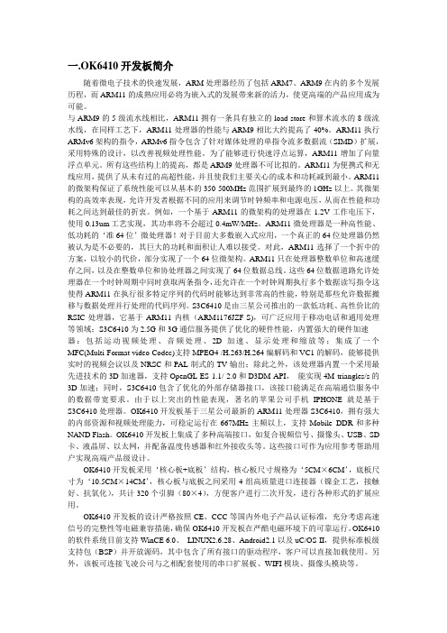
一.OK6410开发板简介随着微电子技术的快速发展,ARM处理器经历了包括ARM7、ARM9在内的多个发展历程,而ARM11的成熟应用必将为嵌入式的发展带来新的活力,使更高端的产品应用成为可能。
与ARM9的5级流水线相比,ARM11拥有一条具有独立的load-store和算术流水的8级流水线,在同样工艺下,ARM11处理器的性能与ARM9相比大约提高了40%。
ARM11执行ARMv6架构的指令,ARMv6指令包含了针对媒体处理的单指令流多数据流(SIMD)扩展,采用特殊的设计,以改善视频处理性能。
为了能够进行快速浮点运算,ARM11增加了向量浮点单元。
所有这些结构上的提高,都是ARM9处理器不可比拟的。
ARM11为便携式和无线应用,提供了从未有过的高超性能,并且使我们主要关心的成本和功耗减到最小。
ARM11的微架构保证了系统性能可以从基本的350-500MHz范围扩展到最终的1GHz以上。
其微架构的高效率表现,允许开发者根据不同的应用来调节时钟频率和电源电压,从而在性能和功耗之间达到最佳的折衷。
例如,一个基于ARM11的微架构的处理器在1.2V工作电压下,使用0.13um工艺实现,其功率将不会超过0.4mW/MHz。
ARM11微处理器是一种高性能、低功耗的‘准64位’微处理器!对于目前大多数嵌入式应用,一个真正的64位处理器仍然被认为是不必要的,其巨大的功耗和面积让人难以接受。
对此,ARM11选择了一个折中的方案,以较小的代价,部分实现了一个64位微架构。
ARM11只在处理器整数单位和高速缓存之间,以及在整数单位和协处理器之间实现了64位数据总线。
这些64位数据道路允许处理器在一个时钟周期中同时获取两条指令,还允许在一个时钟周期执行多个数据读写指令这使得ARM11在执行很多特定序列的代码时能够达到非常高的性能,特别是那些允许数据搬移与数据处理并行处理的代码序列。
S3C6410是由三星公司推出的一款低功耗、高性价比的RSIC处理器,它基于ARM11内核(ARM1176JZF-S),可广泛应用于移动电话和通用处理等领域;S3C6410为2.5G和3G通信服务提供了优化的硬件性能,内置强大的硬件加速器:包括运动视频处理、音频处理、2D加速、显示处理和缩放等;集成了一个MFC(Multi-Format video Codec)支持MPEG4 /H.263/H.264编解码和VC1的解码,能够提供实时的视频会议以及NRSC和PAL制式的TV输出;除此之外,该处理器内置一个采用最先进技术的3D加速器,支持OpenGL ES 1.1/ 2.0和D3DM API,能实现4M triangles/s的3D加速;同时,S3C6410包含了优化的外部存储器接口,该接口能满足在高端通信服务中的数据带宽要求。

铁将科技 6410 双系统实验箱 使用手册产品介绍:本实验箱带有Linux (Qt 操作界面)、Android 两种操作系统的实验平台,可以进行Linux 和Android 两种系统下的基础实验以下是实验板布局:初次使用介绍:1、实验箱基本实验环境搭建实验箱的使用需要与计算机搭建出主机和宿主机的实验平台。
在打开实验箱,根据配件清单清点配件完毕之后,就可以搭建实验平台。
首先,确保实验板开关关闭,插上5V 供电电源。
然后,用串口线将计算机和实验板相连(便于在计算机上查看终端输出信息),将Mini USB 线的mini 端插到实验板的Mini USB 接口,将普通的USB 接口插到计算机的USB 接口(需要在计算机上安装Mini USB 驱动,Mini USB 线的作用主要是在烧写u-boot 、kernel 、根文件系统时快速传输上述文件)。
将实验箱配套的网线分别与计算机和实验板之上的网口相连接。
耳机和VGA 连接线可以留待以后进行相关实验之时进行连接。
2、启动系统类别的选择实验箱出厂之时,默认是烧写好相关bootloader、kernel以及根文件系统的,掰开开关,即可让实验板启动,在开机时按住HOME键(红色按钮),系统会进入Linux系统Qt界面平台,在不按HOME键的情况下,实验板自动进入Android系统。
3、查看系统终端输出信息在插好串口线的情况下,打开SecureCRT软件,如下图所示:单击左数第一个“连接”按钮,出现如图所示对话框:单击左数第三个“新建连接”按钮,出现新建连接对话框,首先要选择的是协议,本实验箱协议选择的是Serial协议,然后下一步。
端口选择要根据自己的计算机(在“我的电脑”属性中,硬件中查看),波特率选择115200,数据位是8,奇偶校验位是None,停止位是1,流控制的三项都不选。
然后单击下一步,为自己新建的会话重命名一个名字,方便自己以后连接。
4、实验板SD卡槽初始核心板中是没有bootloader的,所以,要用SD卡启动(在SD卡中做了一个启动用的U-boot),此外,还可以在SD卡中存储数据。
OK6410裸机程序---leds
今天写一下OK6410 裸机中的led 灯,led 是差不最简单的裸机驱动了吧。
详细的说一下,以便梳理自己的知识。
我们首先看一下OK6410 的LED 连接图:
其中NLED1234,和s3c6410 的GPIO 引脚相连,如图:
其实LED 发光的原理很简单的,就是把LED 连接到s3c6410 的GPIO 引脚,通过改变s3c6410 的GPIO 上的电平来控制LED 发光。
这样的话就很清楚了,我们来看下s3c6410 datasheet 上关于GPIO 引脚的设置:
首先是GPMCON 寄存器:
因为我们要控制GPIO 的电平,所以要把对应的GPIO 引脚设置为Output,即:0001
像我们这个就是:GPMCON &=0xffff fff1;
把这个引脚设置好后,我们可以通过改变GPMDAT 的值来改变引脚上的电平。
下面是GPMDAT:
可以看出来我们只要把对应的位设置为0 或1,就可以控制LED 了。
简单吧?下面看下源程序:。
OK6410开发板启动模式介绍平台:ARM11 三星S3C6410开发板:飞凌OK6410-A开发板…OM0‟信号为S3C6410芯片时钟源选择信号,当…OM0‟信号为“0”时选择…XTlpll‟:当…OM0‟信号为“1”时选择…EXTCLK‟。
这里,OK6410开发板使用…XTlpll‟,所以…OM0‟直接下拉接地。
…SELNAND‟信号用来选择系统FLASH存储器类型,当选择NAND FLASH时必须为高电平…1‟,选择ONENAND存储器时为低电平…0‟,OK6410开发板使用NAND FLASH存储器,所以这里直接上接为高。
…EINT13-EINT15‟为IROM启动方式设备选择引脚,当使用IROM启动方式时,S3C6410处理器首先运行片内ROM固化程序,读取EINT15、EINT14、EINT13三个端口引脚状态,再根据本配置的不同状态,从而选择不同的设备启动。
OM1-OM4信号为S3C6410处理器启动方式配置引脚。
目前的ARM处理器都支持多种启动模式,S3C6410和以前的Samsung的ARM处理器一样,通过外部管脚OM[4:0]的拉高拉低来决定是从哪个存储设备上启动。
我认为S3C6410的User Manual 并没有说的很清楚,所以我在最开始使用的时候,也对其启动模式有一些误解,下面就我个人的理解,介绍一下S3C6410的启动。
先读一下S3C6410 User Manual的第3章System Controller,在123页列了一张表,如图:这章表列出了S3C6410所支持的几种启动模式。
首先介绍一下和启动模式相关的硬件管脚:OM[4:0]:选择启动设备及时钟源。
OM[0]为0选择XXTlpll,为1选择XEXTCLK。
GPN[15:13]:用于识别所支持的Nandflash的类型,包括Page的类型和地址周期。
XSELNAND:选择Nand启动或者是OneNand启动。
OK6410的裸机调试(不用Jlink)废话不多说,直接进入主题。
有两种方法写入,一种是从sd卡启动,一种是从nand flash中启动。
方法一:用sd卡启动我们的裸机程序用到的软件:WinHex_14.0_SR-1_SC.exe首先在RVDS上编译裸机代码,RVDS的设置可以参考我的设置,(好像不这么设置也可以成功)我的这项设置输出的是文件名为zImage的二进制代码文件。
注意是zImage!!没有.bin!之后一种方法就用到它,暂且先说了吧。
插入已经格式化的SD卡,打开WinHex_14.0_SR-1_SC.exe这个软件。
S3C6410 SD 启动模式原理: 上电后,CPU自动将SD0丛最后0x23FF 处,连续8KB数据读到内部SRAM 0x0C000000处执行.就这样,我们的裸奔程序就写到SD卡中了,把OK6410设置为SD卡启动,就可以看到我们的裸机程序在运行了!方法二:借助uboot把我们的裸机程序从nand flash中启动起来!我们一键烧写的方法,将SD做一些准备。
打开SD_Writer.exe然后把uboot.bin拷贝到H盘中(SD卡的盘符)可以用位于OK6410-A 6410官方基础资料-2G\linux2.6.28\demo下的uboot.bin 接下来把我们刚刚生成的裸机目标文件“zImage”拷贝到SD卡中。
设置OK6410为SD卡启动,用dnw观察打印的信息,看到此信息就说明烧写完成了。
完成后把板子设置为nandflash启动,就可以“裸奔”了看到这个信息就说明你的裸机程序在执行了总结方法一借鉴了别人的想法,方法二是本人自己摸索出来的!大家一起学习,一同进步!DIY爱好者2011年6月20日。