AT88SC系列完整文档,带通信协议,怎么用,方法,教程,中文资料,中文文档AT88SC0104CA
- 格式:pdf
- 大小:1.23 MB
- 文档页数:79

AT88SC0104C芯片和DS28E01芯片类似,该加密芯片与CPU进行交互认证,实现系统的防拷贝,该加密芯片内部配置数据基本无法获取,与CPU间通信采用密文方式。
安全性较好。
天大创芯利用各种技术保护配置数据—OTP (反熔丝、基于闪存的可重复编程存储单元以及可重复编程、基于SRAM的可配置逻辑单元。
由于配置数据存储于AT88SC0104C解密芯片,并且芯片具有防止存储数据读取的机制基于闪存的解决方案都提供了相对安全的方案。
此外,除非采用非常复杂的方法来使安全机制失效,否则数据遭到破坏的可能性非常低AT88SC168保密性能强,读写速度快,无需先擦除就可以进行写操作。
AT88SC1608加密卡时钟频率为1MHz,支持页写方式(16字节/页),如果以页写方式访问的话,访问时间为10ms(最大)/页;工作电压为2.7V—5.5V;写/擦除次数为10万次;数据保持100年;工作温度为0—70℃;通讯协议符合ISO/IEC 7816-3同步协议。
尤其是AT88SC1608加密卡的高保密性能十分突出,除了带加密逻辑,还具有高保密认证及反截取跟踪技术,64位相互认证及认证错误计数器,错误计数8次。
AT88SC1608具有1个128字节设置区和8个256字节应用分区,8个区可以自由合并,分别受读密码、写密码(16套密码、各3个字节)控制,错误计数8次。
下面将利用本加密芯片进行产品加密的最安全模式的原理及其实现过程进行阐述。
1)芯片的认证:通过读取芯片配置区内的序列号,制造商ID以及加密的存储区,获得数据进行64位密钥的运算(自制的F1算法),得到芯片内部的加密种子Gc。
再获得芯片内部的特定寄存器的随机数Ci 和CPU产生的随机数Q1,利用芯片内部的F2算法,芯片和CPU 分别进行F2(Ci,Q1,Gc)运算,利用计算结果进行双向判断,从而完成认证2)芯片的加密认证:芯片认证完成后,采用第一步运算产生的SK(F2算法特定处的中间结果),以及由认证更新过得Ci+1 和CPU产生的随机数Q2再进行一次加密运算F2(Ci+1,Q2,SK)认证,最后再通过读取芯片内部更新的Ci+2与CPU计算的结果进行比较,如果相同,则加密认证完成,进入加密模式。
摘要:本文首先介绍了GSM移动通信中的收发短消息(SMS)协议及其编码方式,接着分别探讨了AT8 9C55微处理器与Motorola D15短消息模块发送、接收接口子程序的设计,并给出了详细的MCS-51编码程序。
关键词:SMS编码;GSM;AT89C55;Motorola D151.0 引言GSM(Global System for Mobile communication)系统是目前基于时分多址技术的移动通讯体制中比较成熟、完善、应用较广泛的一种系统,主要提供话音、短信息、数据等多种业务。
基于GSM短消息功能可以做成传输各种检测、监控数据信号和控制命令的数据通信系统,无需另外组建专用通信网络,被广泛用于远程监控、定位导航、个人通信终端等场合。
Motorola D15是带语音,数据,传真和短消息支持的PHASE II GSM四类嵌入式封装的模块,常应用于导航,紧急服务,安全系统等领域。
数据应用能提供包括车载信息,移动计算,资产管理,远程咪表读取,街灯控制,家庭安全,销售管理,法事管理,POS连接,家用器具监视和控制,显示系统,装入管理等功能。
本文以Motorola D15模块为例,探讨了AT89C55微处理器与Motorola D15短消息模块发送、接收接口子程序的具体实现过程。
1.1 SMS协议及其编码方式GSM移动通信中的短消息传输主要有以下3种类型:①分组模式(Block Mode)。
该模式是最早期的短消息传输方式,其通信效率最低。
②文本模式(Text Mode)。
Motorola D15不支持该模式。
③PD U(Protocol Date Unit)模式(PDU模式)。
该模式是当前短消息协议中被广泛使用的模式。
欧洲ETS(Electronic Telegraph System电报系统)协会规定:通过GSM数字蜂窝移动通信网络来发送短消息,用户数据必须转化为GSM字符。
而且,用户数据的内容必须是ASCII码字符集里的0x00到0x7f,7位编码的字符(这是对于英文短消息的规定)。
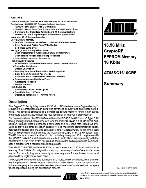
Note: This is a summary document. A complete document is available under NDA. For more information, please contact your local Atmel sales office.Features•One of a Family of Devices with User Memory of 1 Kbit to 64 Kbits •Contactless 13.56 MHz RF Communications Interface–ISO/IEC 14443-2:2001 Type B Compliant–ISO/IEC 14443-3:2001 Type B Compliant Anticollision Protocol –Command Set Optimized for Multicard RF Communications –Tolerant of Type A Signaling for Multiprotocol Applications •Integrated 82 pF Tuning Capacitor •User EEPROM Memory–16 Kbits Configured as Sixteen 128-byte (1-Kbit) User Zones –Byte, Page, and Partial Page Write Modes –Self-timed Write Cycle•256-byte (2-Kbit) Configuration Zone–User-programmable Application Family Identifier (AFI)–User-defined Anticollision Polling Response –User-defined Keys and Passwords •High-Security Features–64-bit Mutual Authentication Protocol (under license of ELVA)–Encrypted Checksum –Stream Encryption–Four Key Sets for Authentication and Encryption –Eight Sets of Two 24-bit Passwords–Password and Authentication Attempts Counters –Selectable Access Rights by Zone –Antitearing Function –Tamper Sensors •High Reliability–Endurance: 100,000 Write Cycles –Data Retention: 10 Years–Operating Temperature: −40°C to +85°CDescriptionThe CryptoRF ® family integrates a 13.56 MHz RF interface into a CryptoMemory ®,resulting in a contactless smart card with advanced security and cryptographic fea-tures. This device is optimized as a contactless secure memory, for RF smart cards,and secure data storage, without the requirement of an internal microprocessor.For communications, the RF interface utilizes the ISO/IEC 14443-2 and -3 Type B bit timing and signal modulation schemes, and the ISO/IEC 14443-3 Slot-MARKER Anti-collision Protocol. Data is exchanged half duplex at a 106-kbit/s rate, with a two-byte CRC_B providing error detection capability. The maximum communication range between the reader antenna and contactless card is approximately 10 cm when used with an RFID reader that transmits the maximum ISO/IEC 14443-2 RF power level.The RF interface powers the other circuits; no battery is required. Full compliance with the ISO/IEC 14443-2 and -3 standards results in anticollision interoperability with the AT88RF020 2-Kbit RFID EEPROM product and provides both a proven RF communi-cation interface and a robust anticollision protocol.The AT88SC1616CRF contains 16 Kbits of user memory and 2 Kbits of configuration memory. The 2 Kbits of configuration memory contain eight sets of read/write pass-words, four crypto key sets, security access registers for each user zone, and password/key registers for each zone.The CryptoRF command set is optimized for a multicard RF communications environ-ment. A programmable AFI register allows this IC to be used in numerous applications in the same geographic area with seamless discrimination of cards assigned to a par-ticular application during the anticollision process.2AT88SC1616CRF5026CS–CRRF–12/06Block DiagramFigure 1. Block Diagram CommunicationsAll personalization and communication with this device is performed through the RF interface. The IC includes an integrated tuning capacitor, enabling it to operate with only the addition of a single external coil antenna.The RF communications interface is fully compliant with the electrical signaling and RF power specifications in ISO/IEC 14443-2:2001 for Type B only. Anticollision operation and frame formatting are compliant with ISO/IEC 14443-3:2001 for Type B only.ISO/IEC 14443 nomenclature is used in this specification where applicable. The following abbreviations are utilized throughout this document. Additional terms are defined in the section in which they are used.•PCD – Proximity Coupling Device: the reader/writer and antenna•PICC – Proximity Integrated Circuit Card: the tag/card containing the IC and antenna•RFU – Reserved for Future Use: any feature, memory location, or bit that is held as reserved for future use•$ xx – Hexadecimal Number: denotes a hex number “xx” (Most Significant Bit on left)Anticollision ProtocolWhen the PICC enters the 13.56 MHz RF field of the host reader (PCD), it performs a power on reset (POR) function and waits silently for a valid Type B polling command.The CryptoRF PICC processes the antitearing registers as part of the POR process. The PCD initiates the anticollision process by issuing an REQB or WUPB command.The WUPB command activates any card (PICC) in the field with a matching AFI code.3AT88SC1616CRF5026CS–CRRF–12/06The REQB command performs the same function but does not affect a PICC in the Halt state. The CryptoRF command set is available only after the anticollision process has been completed.CRC Error DetectionA two-byte CRC_B is required in each frame transmitted by the PICC or PCD to permit transmission error detection. The CRC_B is calculated on all of the command and data bytes in the frame. The SOF, EOF, start bits, stop bits, and EGT are not included in the CRC_B calculation. The two-byte CRC_B follows the data bytes in the frame.Figure 2. Location of the Two CRC_B Bytes within a FrameType A ToleranceThe RF Interface is designed for use in multiprotocol applications. It will not latch or lock up if exposed to Type A signals and will not respond to them. The PICC may reset in thepresence of Type A field modulation but is not damaged by exposure to Type A signals.4AT88SC1616CRF5026CS–CRRF–12/06User MemoryThe EEPROM user memory is divided into 16 user zones as shown in the memory map in Table 1. Multiple zones allow for different types of data or files to be stored in different zones. Access to the user zones is allowed only after security requirements have been met. These security requirements are defined by the user in the configuration memory during personalization of the device. The EEPROM memory page length is 16 bytes.Configuration MemoryThe configuration memory consists of 2048 bits of EEPROM memory used for storing system data, passwords, keys, codes, and security-level definitions for each user zone.Access rights to the configuration zone are defined in the control logic and may not be altered by the user. These access rights include the ability to program certain portions of the configuration memory and then lock the data written through use of the security fuses.Security FusesThere are three fuses on the device that must be blown during the device personaliza-tion process. Each fuse locks certain portions of the configuration memory as OTP memory. Fuses are designated for the module manufacturer, card manufacturer and card issuer and must be blown in sequence.Table 1. Memory MapZone$0$1$2$3$4$5$6$7User 0$00–128 Bytes–$78User 1–––User 14$00––$78User 15$00–128 Bytes–$785AT88SC1616CRF5026CS–CRRF–12/06Communication SecurityCommunication between the PICC and reader operates in three basic modes. Standard mode is the default mode for the device after power-up and anticollision. Authentication mode is activated by a successful authentication sequence. Encryption mode is activated by a successful encryption activation, following a successful authentication.Notes:1.Modification Detection Code2.Message Authentication CodeSecurity MethodologyFigure 3. Security MethodologyMemory AccessDepending on the device configuration, the host will carry out the authentication protocol and/or present different passwords for each operation: read or write. To insure security between the different user zones (multiapplication card), each zone can use a different set of passwords. A specific attempts counter for each password and for the authentication provides protection against systematic attacks.Table 2. Configuration Security ModesMode User Data PasswordsData IntegrityCheckStandard clear clear MDC (1)Authentication clear encrypted MAC (2)Encryption encryptedencryptedMAC (2)6AT88SC1616CRF5026CS–CRRF–12/06Security OperationsAntitearingIn the event of a power loss during a write cycle, the integrity of the device’s stored data may be recovered. This function is optional: the host may choose to activate the antitearing function depending on application requirements. When antitearing is active,write commands take longer to execute since more write cycles are required to complete them. Data writes are limited to 8-byte pages when antitearing is active.Data is written first to a buffer zone in EEPROM instead of to the intended destination address, but with the same access conditions. The data is then written to the required location. If this second write cycle is interrupted due to a power loss, the device will automatically recover the data from the buffer zone at the next power-up.Password VerificationPasswords may be used to protect user zone read and/or write access. When a password is presented using the Check Password command, it is memorized and active until power is removed unless a new password is presented or a valid DESELECT or IDLE command is received. Only one password is active at a time, but write passwords also give read access.Authentication ProtocolThe access to a user zone may be protected by an authentication protocol in addition to password dependent rights. Passwords are encrypted in authentication mode.The authentication success is memorized and active as long as the chip is powered,unless a new authentication is initialized or a valid DESELECT or IDLE command is received. If the new authentication request is not validated, the card loses its previous authentication and it must be presented again. Only the last request is memorized.EncryptionThe data exchanged between the card and the reader during Read, Write, and Check Password commands may be encrypted to ensure data confidentiality.The issuer may choose to protect the access to a user zone with an encryption key by settings made in the configuration memory. In that case, activation of the encryption mode is required in order to read/write data in the zone.The encryption activation success is memorized and active as long as the chip is powered, unless a new initialization is initiated or a valid DESELECT or IDLE command is received. If the new encryption activation request is not validated, the card will no longer encrypt data during read operations nor will it decrypt data received during write or Check Password operations.ChecksumThe PICC implements a data validity check function in the form of a checksum. The checksum may function in standard or cryptographic mode. In the standard mode, the checksum is optional and may be used for transmission error detection. The cryptographic mode is more powerful since it provides data origin authentication capability in the form of a Message Authentication Code (MAC). To write data to the device, the host is required to compute a valid MAC and provide it to the device.If after an ingoing command the device computes a MAC different from the MAC transmitted by the host, not only is the command abandoned but the cryptographic mode is also reset.A new authentication is required to reactivate the cryptographic mode.Initial Device ProgrammingCryptoRF is delivered with all security features disabled. To program the polling response or enable the security features of CryptoRF the device must be personalized by programming several registers. This is accomplished by programming the configuration memory using simple write and read commands.7AT88SC1616CRF5026CS–CRRF–12/06Transport PasswordTo gain access to the configuration memory, a transport password known as the secure code must be presented using the Check Password command. The secure code for AT88SC1616CRF is $50 44 72.Tuning Capacitance The capacitance between the coil pins AC1 and AC2 is 82 pF nominal and may vary ±10% over temperature and process variation.ReliabilityMechanicalEngineering SamplesTable 3. ReliabilityParameter Min Typ Max Units Write endurance 100,000––Write Cycles Data retention10––YearsSample Code Sample DescriptionMaximum RangeAT88SC1616CRF-MR1R Module, 82 pF, on 35 mm tape AT88SC1616CRF-L01B RF Smart Card, ID-1 size, PVC8−10 cm AT88SC1616CRF-MU1RFID Tag, 17 mm diameter, on 35 mm tape 1−3 cm AT88SC1616CRF-MS1RFID Tag, 10 x 20 mm size, on 35 mm tape10−15 mm8AT88SC1616CRF5026CS–CRRF–12/06Ordering InformationPackaging InformationOrdering Code Package Tuning CapacitorTemperature Range AT88SC1616CRF-MR1R Module82 pF Commercial (0° C to 70° C)AT88SC1616CRF-WA16 mil wafer, 150 mm diameter82 pFIndustrial (−40° C to 85° C)Package Type DescriptionR Module2- lead RF Smart Card Module, XOA2 style, RoHS compliantDisclaimer: The information in this document is provided in connection with Atmel products. No license, express or implied, by estoppel or otherwise,to any intellectual property right is granted by this document or in connection with the sale of Atmel products. EXCEPT AS SET FORTH IN ATMEL’S TERMS AND CONDI-TIONS OF SALE LOCATED ON ATMEL’S WEB SITE, ATMEL ASSUMES NO LIABILITY WHATSOEVER AND DISCLAIMS ANY EXPRESS, IMPLIED OR STATUTORY WARRANTY RELATING TO ITS PRODUCTS INCLUDING, BUT NOT LIMITED TO, THE IMPLIED WARRANTY OF MERCHANTABILITY, FITNESS FOR A PARTICULAR PURPOSE, OR NON-INFRINGEMENT. IN NO EVENT SHALL ATMEL BE LIABLE FOR ANY DIRECT, INDIRECT, CONSEQUENTIAL, PUNITIVE, SPECIAL OR INCIDEN-TAL DAMAGES (INCLUDING, WITHOUT LIMITATION, DAMAGES FOR LOSS OF PROFITS, BUSINESS INTERRUPTION, OR LOSS OF INFORMATION) ARISING OUT OF THE USE OR INABILITY TO USE THIS DOCUMENT, EVEN IF ATMEL HAS BEEN ADVISED OF THE POSSIBILITY OF SUCH DAMAGES. Atmel makes no representations or warranties with respect to the accuracy or completeness of the contents of this document and reserves the right to make changes to specifications and product descriptions at any time without notice. Atmel does not make any commitment to update the information contained herein. Unless specifically provided otherwise, Atmel products are not suitable for, and shall not be used in, automotive applications. Atmel’s products are not intended, authorized, or warranted for use as components in applications intended to support or sustain life.Atmel CorporationAtmel Operations2325 Orchard Parkway San Jose, CA 95131, USA Tel: 1(408) 441-0311Fax: 1(408) 487-2600Regional HeadquartersEuropeAtmel SarlRoute des Arsenaux 41Case Postale 80CH-1705 Fribourg SwitzerlandTel: (41) 26-426-5555Fax: (41) 26-426-5500AsiaRoom 1219Chinachem Golden Plaza 77 Mody Road Tsimshatsui East Kowloon Hong KongTel: (852) 2721-9778Fax: (852) 2722-1369Japan9F, Tonetsu Shinkawa Bldg.1-24-8 ShinkawaChuo-ku, Tokyo 104-0033JapanTel: (81) 3-3523-3551Fax: (81) 3-3523-7581Memory2325 Orchard Parkway San Jose, CA 95131, USA Tel: 1(408) 441-0311Fax: 1(408) 436-4314Microcontrollers2325 Orchard Parkway San Jose, CA 95131, USA Tel: 1(408) 441-0311Fax: 1(408) 436-4314La Chantrerie BP 7060244306 Nantes Cedex 3, France Tel: (33) 2-40-18-18-18Fax: (33) 2-40-18-19-60ASIC/ASSP/Smart CardsZone Industrielle13106 Rousset Cedex, France Tel: (33) 4-42-53-60-00Fax: (33) 4-42-53-60-011150 East Cheyenne Mtn. Blvd.Colorado Springs, CO 80906, USA Tel: 1(719) 576-3300Fax: 1(719) 540-1759Scottish Enterprise Technology Park Maxwell BuildingEast Kilbride G75 0QR, Scotland Tel: (44) 1355-803-000Fax: (44) 1355-242-743RF/AutomotiveTheresienstrasse 2Postfach 353574025 Heilbronn, Germany Tel: (49) 71-31-67-0Fax: (49) 71-31-67-23401150 East Cheyenne Mtn. Blvd.Colorado Springs, CO 80906, USA Tel: 1(719) 576-3300Fax: 1(719) 540-1759Biometrics/Imaging/Hi-Rel MPU/High Speed Converters/RF DatacomAvenue de Rochepleine BP 12338521 Saint-Egreve Cedex, France Tel: (33) 4-76-58-47-50Fax: (33) 4-76-58-47-60Literature Requests/literature5026CS–CRRF–12/06©2006 Atmel Corporation. All rights reserved. Atmel ®, logo and combinations thereof, Everywhere You Are ®, CryptoMemory ®, CryptoRF ® and others are registered trademarks or trademarks of Atmel Corporation or its subsidiaries. Other terms and product names may be trademarks of others.。

A T24C256中文资料2009-11-15 09:43特性与1MHz I2C 总线兼容1.8 到6.0 伏工作电压范围低功耗CMOS 技术写保护功能当WP 为高电平时进入写保护状态64 字节页写缓冲器自定时擦写周期100,000 编程/擦写周期可保存数据100 年8 脚DIP SOIC 封装温度范围商业级工业级和汽车级概述CAT24WC256 是一个256K 位串行CMOS E2PROM 内部含有32768 个字节每字节为8 位CATALYST 公司的先进CMOS 技术实质上减少了器件的功耗CAT24WC256 有一个64 字节页写缓冲器该器件通过I2C 总线接口进行操作管脚描述管脚名称功能A0 A1 地址输入SDA 串行数据/地址SCL 串行时钟WP 写保护Vcc +1.8V 6.0V 电源Vss 地NC 未连接极限参数工作温度工业级-55 +125商业级0 +75贮存温度-65 +150各管脚承受电压-2.0V Vcc+2.0VVcc 管脚承受电压-2.0V +7.0V封装功率损耗Ta=25 1.0W焊接温度(10 秒) 300口输出短路电流100mA功能描述CAT24WC256 支持I2C 总线数据传送协议I2C 总线协议规定任何将数据传送到总线的器件作为发送器任何从总线接收数据的器件为接收器数据传送是由产生串行时钟和所有起始停止信号的主器件控制的CAT24WC256 是作为从器件被操作的主器件和从器件都可以作为发送器或接收器但由主器件控制传送数据发送或接收的模式管脚描述SCL 串行时钟CAT24WC256 串行时钟输入管脚用于产生器件所有数据发送或接收的时钟这是一个输入管脚SDA 串行数据/地址双向串行数据/地址管脚用于器件所有数据的发送或接收SDA 是一个开漏输出管脚可与其它开漏输出或集电极开路输出进行线或wire-ORWP 写保护当WP 脚连接到Vcc 所有内存变成写保护只能读当WP 引脚连接到Vss 或悬空允许器件进行读/写操作A0 A1 器件地址输入这些管脚为硬连线或者不连接对于单总线系统最多可寻址4 个CAT24WC256 器件参阅器件寻址当这些引脚没有连接时其默认值为0I2C 总线协议I2C 总线协议定义如下1 只有在总线空闲时才允许启动数据传送2 在数据传送过程中当时钟线为高电平时数据线必须保持稳定状态不允许有跳变时钟线为高电平时数据线的任何电平变化将被看作总线的起始或停止信号起始信号时钟线保持高电平期间数据线电平从高到低的跳变作为I2C 总线的起始信号停止信号时钟线保持高电平期间数据线电平从低到高的跳变作为I2C 总线的停止信号器件寻址主器件通过发送一个起始信号启动发送过程然后发送它所要寻址的从器件的地址8 位从器件地址的高5 位固定为10100 见图5 接下来的2 位A1 A0 为器件的地址位最多可以连接4 个器件到同一总线上这些位必须与硬连线输入脚A1 A0 相对应从器件地址的最低位作为读写控制位1表示对从器件进行读操作0 表示对从器件进行写操作在主器件发送起始信号和从器件地址字节后CAT24WC256 监视总线并当其地址与发送的从地址相符时响应一个应答信号通过SDA 线CAT24WC256 再根据读写控制位R/W 的状态进行读或写操作应答信号I2C 总线数据传送时每成功地传送一个字节数据后接收器都必须产生一个应答信号应答的器件在第9 个时钟周期时将SDA 线拉低表示其已收到一个8 位数据CAT24WC256 在接收到起始信号和从器件地址之后响应一个应答信号如果器件已选择了写操作则在每接收一个8 位字节之后响应一个应答信号当CAT24WC256 工作于读模式时在发送一个8 位数据后释放SDA 线并监视一个应答信号一旦接收到应答信号CAT24WC256 继续发送数据如主器件没有发送应答信号器件停止传送数据并等待一个停止信号写操作字节写在字节写模式下主器件发送起始信号和从器件地址信息R/W 位置0 给从器件在从器件送回应答信号后主器件发送两个8 位地址字写入CAT24WC256 的地址指针主器件在收到从器件的应答信号后再发送数据到被寻址的存储单元CAT24WC256 再次应答并在主器件产生停止信号后开始内部数据的擦写在内部擦写过程中CAT24WC256 不再应答主器件的任何请求页写在页写模式下单个写周期内CAT24WC256 最多可以写入64 个字节数据页写操作的启动和字节写一样不同在于传送了一字节数据后主器件允许继续发送63 个字节每发送一个字节后CAT24WC256 将响应一个应答位且内部低6 位地址加1 高位地址保持不变如果主器件在发送停止信号之前发送大于64 个字节地址计数器将自动翻转先前写入的数据被覆盖当所有64 字节接收完毕主器件发送停止信号内部编程周期开始此时所有接收到的数据在单个写周期内写入CAT24WC256应答查询可以利用内部写周期时禁止数据输入这一特性一旦主器件发送停止位指示主器件操作结束时CAT24WC256 启动内部写周期应答查询立即启动包括发送一个起始信号和进行写操作的从器件地址如果CAT24WC256 正在进行内部写操作将不会发送应答信号如果CAT24WC256 已经完成了内部写操作将发送一个应答信号主器件可以继续对CAT24WC256 进行下一次读写操作写保护写保护操作特性可使用户避免由于不当操作而造成对存储区域内部数据的改写当WP 管脚接高时整个寄存器区全部被保护起来而变为只可读取CAT24WC256 可以接收从器件地址和字节地址但是装置在接收到第一个数据字节后不发送应答信号从而避免寄存器区域被编程改写读操作CAT24WC256 读操作的初始化方式和写操作时一样仅把R/W 位置为1 有三种不同的读操作方式立即/当前地址读选择/随机读和连续读立即/当前地址读的地址计数器内容为最后操作字节的地址加1 也就是说如果上次读/写的操作地址为N 则立即读的地址从地址N+1 开始如果N=E 此处E=32767 则计数器将翻转到0 且继续输出数据CAT24WC256接收到从器件地址信号后R/W 位置1 它首先发送一个应答信号然后发送一个8 位字节数据主器件不需发送一个应答信号但要产生一个停止信号选择/随机读选择/随机读操作允许主器件对寄存器的任意字节进行读操作主器件首先通过发送起始信号从器件地址和它想读取的字节数据的地址执行一个伪写操作在CAT24WC256 应答之后主器件重新发送起始信号和从器件地址此时R/W 位置1 CAT24WC256 响应并发送应答信号然后输出所要求的一个8 位字节数据主器件不发送应答信号但产生一个停止信号连续读连续读操作可通过立即读或选择性读操作启动在CAT24WC256 发送完一个8 位字节数据后主器件产生一个应答信号来响应告知CAT24WC256 主器件要求更多的数据对应每个主机产生的应答信号CAT24WC256 将发送一个8 位数据字节当主器件不发送应答信号而发送停止位时结束此操作从CAT24WC256 输出的数据按顺序由N 到N+1 输出读操作时地址计数器在CAT24WC256 整个地址内增加这样整个寄存器区域在可在一个读操作内全部读出当读取的字节超过E 此处E=32767计数器将翻转到零并继续输出数据字节。
YX-SC880智能数据采集器用户手册型号:SC880 操作前请仔细阅读该手册,其中包括产品技术、性能、使用、维修保养等方面内容。
欢迎使用欢迎您使用SC880智能数据采集器。
很高兴向您介绍SC880智能数据采集器,愿SC880智能数据采集器能够帮助您轻松、高效的工作。
SC880是一款具有多种行业应用功能的智能数据采集器,它基于Microsoft Windows Mobile 6.5操作系统,在结合了智能数据采集器通讯功能和高性能的掌上电脑来轻松管理个人和工作信息的功能。
不仅如此,通过高速的 GPRS 技术,它可以使您畅游在信息高速公路上。
SC880数据存储具有高安全性,不会因电量耗尽而丢失。
SC880具有符合GB/T 4208规定的IP65防护等级的牢固的外壳、艳丽的彩色屏幕、内置的实用软件,轻松地操作,将会给您良好的使用体验。
SC880内置了高性能的工业级320万像素摄像头。
本手册系统地介绍了如何使用 SC880的各种功能、使用技巧以及注意事项,请在使用前仔细阅读手册,以便快速掌握使用方法。
版权说明Microsoft、Windows、Windows徽标、Outlook 和ActiveSync 是Microsoft Corporation 在美国和其它国家 / 地区的商标。
microSD™是SD卡片协会商标。
本文档中提及所有其它产品名称可能是其各自所属公司的商标。
本公司对本文档中出现的技术错误、编辑错误或遗漏之处概不负责。
本信息按“原样”提供且不作任何保证。
如有更改,恕不另行通知。
本文档包含的所有权信息受版权保护。
未经本公司事先书面许可,不得影印、复制本文档的任何部分或将其翻译成其它语言。
本文所含信息可能随时更改,恕不另行通知。
本公司产品和服务的唯一保修条款均在此产品和服务随附的保修声明中明确阐明。
此处任何信息均不构成额外的保修条款。
本公司对于本文包含的技术或编辑错误或遗漏概不负责。
微软、Windows 和Windows标识均为微软公司在美国或其他国家的注册商标或商标。
SC-RWP2-USB型AT88SCxx读写编程器使用说明1.简介本读写编程器适用于AT88SCxx系列加密器件的开发,具有读写配置区、读写用户、模拟认证、配置文件管理和脱机编程等功能。
在熔丝已熔断(在FUSES=#00H)的情况下,只要导入了正确的密钥(Gc和Password),还可将器件所有数据和配置文件读回。
2.硬件简介读写编程器硬件示意图如图所示。
USB接口:安装时,用USB数据线与PC和USB连接。
复位按键(RST):单片机复位编程按键(PROM):启动一次编程测试按键(TEST):用于检测器件安置是否正确。
按下后,如绿灯亮表明通过检测,如不亮则须对器件的安置情况进行检查。
对SO-8封装的器件须检查安置方向和引脚连接情况;清零按键(CLR):使编程计数值清零。
使用时,应同时按下本键和“复位按键(RST)”,然后先释放“复位按键(RST)”才能起作用。
电源开关:拨向“ON”一侧为接通电源。
也可直接使用USB供电。
电源插座:直流输入电压8V~15V。
电源指示(PWR):点亮表明装置电源已接通。
成功指示(OK):点亮表明一次操作成功。
器件电源(CVCC):点亮表明器件已上电。
数码显示:显示已编程器件的计数,计数值断电不丢失。
转换插座:安置时注意PCB板上白色线框。
器件安置:安置时注意PCB板上白色线框注释的1、4、5、8脚。
安置后,应按下“测试按键(TEST)”以检测器件的安置情况,绿灯点亮表明器件安置正确;否则为不正确,须检查器件的安置情况。
3.软件使用方法对AT88SC0104C~25616C各寄存器和数据存储器的配置请参考Atmel公司的有关资料。
3.1 生产配置文件(由已有的配置文件修改生成)1. 由“File”菜单中选择“Lode File”。
如要重新装入配置文件,则应先退出配置区/用户区的操作界面。
2. 由“Device Operations”菜单中选择“Config Zone”,在此对配置区进行配置,按“Leave”按钮退出。