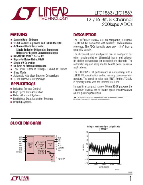
18647231中文资料
- 格式:pdf
- 大小:315.05 KB
- 文档页数:1
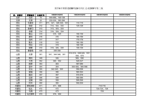

一级简码表一(G)地(F)在(D)要(S)工(A)上(H)是(J)中(K)国(L)同(M)和(T)的(R)有(E)人(W)我(Q)主(Y)产(U)不(I)为(O)这(P)民(N)了(B)发(V)以(C)经(X)二级简码表:GFDSAHJKLMTREWQYUIOPNBVCXG五于天末开下理事画现玫珠表珍列玉平不来与屯妻到互F二寺城霜载直是吉协南才垢圾夫无坟增示赫过志地雪支D三夺大厅左丰百右历成帮原胡春克太磁砂灰达成顾肆友龙S本村枯林械相查可楞机格析极检构术样档杰棕杨李要权楷A七革基苛式牙划或功贡攻匠菜共区芳燕东芝世节切芭药H睛睦睚盯虎止旧占卤贞睡睥肯具餐眩瞳步眯瞎卢眼皮此J量时晨果虹早昌蝇曙遇昨蝗明蛤晚景暗晃显晕电最归紧昆K呈叶顺呆呀中虽吕另员呼听吸只史嘛啼吵噗喧叫啊哪吧哟L车轩因困轼四辊加男轴力斩胃办罗罚较辚边思囝轨轻累M同财央朵曲由则崭册几贩骨内风凡赠峭赕迪岂邮凤嶷T生行知条长处得各力向笔物秀答称入科秒秋管秘季委么第R后持拓打找年提扣押抽手折扔失换扩拉朱搂近所报扫反批E且肝须采肛胩胆肿肋肌用遥朋脸胸及胶膛膦爱甩服妥肥脂W全会估休代个介保佃仙作伯仍从你信们偿伙亿他分公化Q钱针然钉氏外旬名锣负儿铁角欠多久匀乐炙锭包凶争色Y主计庆订度让刘训为高放诉衣认义方说就变这记离良充率U闰半关亲并站间部曾商产瓣前闪交六立冰普帝决闻妆冯北I汪法尖洒江小浊澡渐没少泊肖兴光注洋水淡学沁池当汉涨O业灶类灯煤粘烛炽烟灿烽煌粗伙炮米料炒炎迷断籽娄烃糨P定守害宁宽寂审宫军宙客宾家空宛社实宵灾之官字安它N怀导居民收慢避惭届必怕愉懈心习悄屡忱忆敢恨怪尼B卫际承阿陈耻阳职阵出降孤阴队隐防联孙耿辽也子限取陛V姨寻姑杂毁叟旭如舅妯九奶婚妨嫌录灵巡刀好妇妈姆C骊对参骠戏骒台劝观矣牟能难允驻骈驼马邓艰双X线结顷红引旨强细纲张绵级给约纺弱纱继综纪弛绿经比常用1500字(列出了86五笔原版的最简码):以下是常用字1到300的r 一g 是j 在d 了b 不i 和t 有e 大dd 这p 主y 中k 人w 上h 为o 们wu 个wh 地f 用et 工a 时jf 要s 动fcl 国l 产u 以c 我q 到gc 他wb 会wf 作wt 来go 分wv 生tg 对cf 于gf 学ip 下gh 级xe 就yi 年rh 阶bwj 义yq 发v 成dn 部uk 民n 可sk 出bm 能ce 方yy 进fj 同m 行tf 面dm 说yu 种tkh 过fp 命wgkb 度ya 革af 而dmj 多qq 子bb 后rg 自thd 社py 加lk 小ih 机sm 也bn 经x 力lt 线xg 本sg 电jn 高ym 量jg 长ta 党ipk 得tj 实pu 家pe 定pg 深ipw 法if 表ge 着udh 水ii 理gj 化wx 争qv 现gm 所rn 二fg 起fhn 政ght 三dg 好vb 十fgh 战hka 无fq 农pei 使wgkq 性ntg 前ue 等tffu 反rc 体wsg 合wgk 斗ufk 路kht 图ltu 把rcn 结xf 第tx 期adwe 里jfd 正ghd 新usr 开ga 论ywx 之pp 物tr 从ww 当iv 两gmww 些hxf 还gip 天gd 资uqwm 事gk 队bw 批rx 如vk 应yid 形gae 想shn 制rmhj 心ny 样su 干fggh 都ftjb 向tm 变yo 关ud 点hko 育yce 重tgj 其adw 思ln 与gn 间uj 内mw 去fcu 因ld 件wrh 日jjjj 利tjh 相sh 由mh 压dfy 员km 气rnb 业og 代wa 全wg 组xeg 数ovt 果js 导nf 平gu 各tk 基ad 或ak 月eee 毛tfn 然qd 问ukd 比xx 展nae 那vfb 它px 最jb 及ey 外qh 没im 看rhf 治ick 提rj 五gg 解qev 系txi 林ss 者ftj 米oy 群vtk 头udi 意ujn 只kw 明je 四lh 道uthp 马cn 认yw 次uqw 文yygy 通cep 但wjg 条ts 较lu 克dq 又ccc 公wc 孔bnn 领wycm 流iyc 入ty 接ruv 军pl 席yam 位wug 情nge 运fcp 器kkd 并ua 习nu 原dr 油img 立uu 放yt 题jghm 质rfm 指rxj 建vfhp 区aq 验cwg 活itd 众www 很tve 教ftbt 决un 特trf 此hx 常ipkh 石dgtg 强xk 极se 土ffff 少it 己nng 根sve 共aw 直fh 团lft 统xyc 式aa 转lfn 别klj 造tfkp 切av 九vt 你wq 取bc 西sghg 持rf 总ukn 料ou连lpk 任wtf 志fn 观cm 调ymf 么tc 七ag 山mmm 程tkgg 百dj 报rb 更gjq 见mqb 必nt 真fhw 保wk 热rvyo 委tv 手rt 改nty 管tp 处th 将uqf 已nnnn 修wht 支fc 识ykw 病ugm 象qje 几mt 先tfq 老ftx以下是常用字301-500光iq 专fny 什wfh 六uy 型gajf 具hw 示fi 复tjt 安pv 带gkp 每txg 东ai 增fu 则mj 完pfq 风mq 回lkd 南fm 广yygt 劳apl 轮lwx 科tu 北ux 打rs 积tkw 车lg 计yf 给xw 节ab 做wdt 务tl 被puhc 整gkih 联bu 步hi 类od 集wys 号kgn 列gq 温ijl 装ufy 即vcb 毫ypt 轴lm 知td 研dga 单ujfj 色qc 坚jcf 据rnd 速gkip 防by 史kq 拉ru 设ymc 世an 达dp 尔qiu 场fnrt 织xkw 历dl 花awx 受epc 求fiy 传wfny 口kkkk 断on 况ukq 采es 精oge金qqqq 界lwj 品kkk 判udjh 参cd 层nfc 止hh 边lp 清ige 至gcf 万dnv确dqe 究pwv 书nnh 术sy 厂dgt 状udy 须ed 离yb 再gmf 目hhhh 海itx 交uq 且eg 儿qt 青gef 才ft 证ygh 低wqa 越fha 际bf 八wty 试yaa 规fwm斯adwr 近rp 注iy 办lw 布dmh 门uyh 铁qr 需fdm 走fhu 议yyq 县egc 虫jhny 固ldd 除bwt 般tem 引xh 齿hwb 千tfk 胜etg 细xl 影jyie 白rrr 济iyj 格st 效uqt 推rwyg 兵rgw 空pw 配sgn 刀vn 叶kf 率yx 述syp 今wynb 选tfqp 养udyj 话ytd 查sj 差uda 德tfl 半uf 敌tdt 始vck 片thg 施ytb 响ktm 收nh 华wxf 觉ipmq 备tlf 红xa 名qk 续xfn 均fqu 药ax 标sfi 记yn 难cw 存dhb 士fghg 身tmd 测imj 紧jc 液iyw 置lfhf 派ire 准uwy 斤rtt 角qe 降bt 维xwy 板src 许ytf 破dhc 技rfc 端umd 消iie 底yqa 床ysi 田lll 势rvyl 感dgkn 往tyg 神pyj 便wgj 圆lkmi 村sf 构sq 照jvko 容pww 非djd 搞rym 亚gog 磨yssd 族ytt 火ooo以下是常用字501-1500段wdm 算tha 适tdp 讲yfj 按rpv 值wfhg 美ugdu 态dyn 黄amw 易jqr 彪hame 服eb 早jh 班gyt 麦gtu 削iej 信wy 排rdj 台ck 声fnr 该yynw 击fmk 素gxi 张xt 密pnt 害pd 候whn 草ajj 何wsk 树scf 肥ec 继xo 右dk属ntk 市ymhj 径tca 严god 螺jlx 检sw 左da 页dmu 抗rymn 苏alw 显jo苦adf 英amd 快nnw 称tq 坏fgi 移tqq 约xq 巴cnh 材sft 省ith 黑lfo 武gah 培fuk 著aft 河isk 帝up 仅wcy 针qf 怎thfn 植sfhg 京yiu 助egl 升tak 王ggg 眼hv 她vbn 抓rrhy 含wynk 苗alf 副gkl 杂vs 普uo 谈yoo 围lfnh 食wyv 射tmdf 源idr 例wgq 致gcft 酸sgc 旧hj 却fcb 充yc 足khu 短tdg 划aj 剂yjjh 宣pgj 环ggi 落ait 首uth 尺nyi 波ihc 承bd 粉ow 践khg 府ywf 鱼qgf 随bde 考ftg 刻ynt 靠tfkd 够qkqq 满iagw 夫fw 失rw 包qn 住wygg 促wkh 枝sfc 局nnk 菌alt 杆sfh 周mfk 护ryn 岩mdf 师jgm 举iwf 曲ma 春dw 超fhv 元fqb 负qm 砂di 封fffy 换rq 太dy 模saj 贫wvm 减udg 阳bj 扬rnr 江ia 析sr 亩ylf 木ssss 言yyy 球gfi 朝fje 医atd 校suq 古dgh 呢knx 稻tev 宁ps 听kr 唯kwyg 输lwg 滑ime 站uh 另kl 卫bg 字pb 鼓fkuc 刚mqj 写pgn 刘yj 良yv 微tmg 略ltk 范aib 供waw 阿bs 块fnw 某afs 功al 套ddu 限bv 友dc 项adm 余wtu 卷udbb 创wbj 律tvfh 雨fghy 让yh 骨me 远fqp 帮dt 初puv 皮hc 播rtol 优wdn 占hk 死gqx 毒gxgu 伟wfn 季tb 训yk 控rpw 激iry 叫kn 找ra 云fcu 互gx 裂gqje 粮oyv跟khv 粒oug 母xgu 练xan 塞pfjf 钢qmq 顶sdm 策tgm 双cc 留qyvl 误ykg 础dbm 吸ke 阻begg 故dty 寸fghy 盾rfh 晚jq 丝xxg 女vvv 散aet 焊ojf 攻at 株sri 亲us 院bpf 冷uwyc 彻tavn 弹xuj 错qaj 尼nx 商um 视pym 艺anb 灭goi 版thgc 烈gqjo 零fwyc 室pgc 轻lc 血tld 倍wuk 缺rmn 厘djfd 泵diu 察pwfi 绝xqc 富pgk 城fd 冲ukh 喷kfa 壤fyk 简tuj 否gik 柱syg 李sb 望yneg 盘tel 磁du 雄dcw 似wny 困ls 巩amy 益uwl 洲iyt 脱euk 座yww 投rmc 奴vcy 侧wmj 润iugg 盖ugl 挥rpl 距kha 触qejy 星jtg 松swc 送udp 获aqt 兴iw 独qtj 官pn 混ijx 纪xn 依wye 未fii 突pwd 架lks 宽pa 冬tuu 倒wgc 章ujj 湿ijo 偏wyna 纹xyy 吃ktn 执rvy 阀uwa 矿dyt 寨pfjs 责gmu 熟ybv 稳tqv 夺df 硬dgj 价wwj 翻toln 努vcl 甲lhnh 奇dskf 预cbd 职bk 评ygu 读yfn 背uxe 协fl 损rkm 棉srm 侵wvp 灰do 虽kj 矛cbt 厚djb 罗lq 泥inx 辟nku 告tfkf 卵qyt 箱tsh 掌ipkr 氧rnu 恩ldn 爱ep 停wyp 曾ul 溶ipwk 营apk 终xtu 纲xm 孟blf 钱qg 待tffy 尽nyu 俄wtr 缩xpw 沙iit 退vep 陈ba 讨yfy 奋dlf 旋ytn 械sa 载fa 胞eqn 幼xln 剥vijh 哪kv 迫rpd 征tgh 槽sgmj 握rng 担rjg 仍we 呀ka 鲜qgu 吧kc 卡hhu 粗oe 介wj 钻qhk 逐epi 弱xu 脚efcb 圈lud 怕nr 盐fhl 末gs 阴be 丰dh 编xyna 印qgb 蜂jtd 急qvn 拿wgkr 扩ry 伤wtl 飞nui 露fkhk 核synw 缘xxe 游iytb 振rdf 操rkk 央md 伍wgg 域fakg 甚adwn 迅nfp 辉iqpl 异naj 序ycb 免qkq 纸xqa 夜ywt 乡xte 久qy 隶vii 缸rma 夹guw 念wynn 兰uff 映jmd 沟iqc 乙nnl 吗kcg 儒wfd 杀qsu 汽irn 磷doq 艰cv 晶jjj 插rtf 埃fct 燃oqdo 欢cqw 铣qtfq 补puh 演ipg 烧oat 咱kth 语ygk 贵khgm 倾wxd 阵bl 碳dmd 威dgv 附bwf 牙ah 芽aah 永yni 瓦gny 斜wtuf 灌iak 欧aqq 献fmud 顺kd 猪qtfj 腐ywfw 洋iu 请yge 透tep 司ngk 危qdb 括rtd 脉eyni 笑ttd 宜peg 若adk 尾ntf 束gki 壮ufg 暴jaw 企whf 菜ae 穗tgjn 楚ssn 汉ic 愈wgen 绿xv 拖rtb 牛rhk 份wwv 染ivs 既vca 秋to 疗ubk 遍ynm 锻qwd 玉gy 夏dht 尖id 殖gqf 井fjk 费xjm 州ytyh 访yyn 吹kqw 荣aps 铜qmgk 沿imk 替fwf 滚iuc 客pt 召vkf 旱jfj 悟ngkg 刺gmi 脑eyb 措raj 贯xfm 藏adnt 敢nb 令wyc 隙bij 炉oyn 壳fpm 硫dyc 煤oa 迎qbp 铸qdt 粘oh 探rpws 临jty 薄aig 旬qj 善uduk 福pyg 纵xww 择rcf 礼pynn 愿drin 伏wdy 残gqg 雷flf 延thp 句qkd 烟ol 纯xgb 渐il 耕dif 跑khq 泽icf 船temk 慢nj 栽fas 鲁qgj 赤fo 繁txgi 境fuj 潮ifj 横sam 掉rhj 锥qwy 池ib 希qdm 败mty 假wnh 亮ypm 谓yle 托rta 伙wo 哲rrk 怀ng 割pdhj 摆rlf 贡am 呈kg 劲cal 财mf 沉ipm 仪wyq 炼oanw 麻yss 罪ldj 祖pye 息thn 辅lgey 穿pwat 货wxm 销qie 齐yjj 鼠vnu 抽rm 画gl 饲qnnk 龙dx 库ylk 守pf 筑tam 房yny 歌sksw 寒pfj 喜fku 哥sks 蚀qnj 洗itf 废ynty 纳xmw 腹etj 乎tuh 录vi 镜quj 谋yaf 妇vv 恶gogn 脂ex 庄yfd 擦rpwi 险bwg 赞tfqm 钟qkhh 摇rer 典maw 柄sgm 辩uyu 竹ttg 谷wwk 卖fnud 乱tdn 虚hao 桥std 奥tmo 伯wr 赶fhfk 垂tga 途wtp 额ptkm 壁nkuf 截faw 网mqq 野jfc 遗khgp 静geq 弄gaj 挂rffg 妄ynvf 镇qfhw 盛dnnl 耐dmjf 援ref 扎rnn 虑han 键qvfp 归jv 符twf 庆yd 聚bct 摩yssr 绕xat 忙nynn 舞rlg 遇jm 顾db 索fpx 胶eu 羊udj 湖ide 钉qs 仁wfg 音ujf 迹yop 碎dyw 伸wjh 灯os 避nk 泛itp 答tw 亡ynv 勇cel 频hid 皇rgf 柳sqt 哈kwg 揭rjq 甘afd 诺yad 概svc 宪ptf 浓ipe 岛qynm 袭dxy 谁ywyg 洪iaw 谢ytm 炮oq 斑gyg 浇iat 讯ynf 徒tfhy 懂nat 灵vo 蛋nhj 闭uft 孩bynw 释toc 乳ebn 私tcy 银qve 伊wvt 景jy 坦fjg 累lx 匀qu 霉ftxu 杜sfg 乐qi 勒afl 隔bgk 巨and 弯yox 一ggl 招rvk 绍xvk 胡de 呼kt 痛uce 峰mtd 柴hxs 簧tamw 午tfj 跳khi 居nd 尚imkf 丁sgh 秦dwt 稍tie 追wnnp 梁ivw 耗ditn 折rr 碱ddg 殊gqr 岗mmq 挖rpwn 氏qa 刃vyi 堆fwy 赫fof 荷awsk 胸eq 衡tqdh 勤akgl 膜eajd 篇tyna 登wgku 慧dhd 驻cy 案pvs 刊fjh 秧tmdy 缓xef 凸hgm 役tmc 剪uejv 川kthh 雪fv 链qlp 渔iqgg 啦kru 脸ew 户yne 洛itk 勃fpb 盟jel 买nudu 杨sn 宗pfi 焦wyo 旗yta 赛pfjm 滤iha 硅dff 股emc 坐wwf 蒸abi 凝uxt 竟ujq 陷bqv 枪swb 救fiyt 黎tqt 冒jhf 暗ju 洞imgk 犯qtb 筒tmgk 您wqin 弧xrc 宋psu 爆oja 谬ynwe 涂iwt 味kfi 臂nkue 津ivfh 障buj 褐pujn 陆bfm 啊kb 健wvf 尊usg 豆gku 拔rdc 莫ajd 抵rqa 坡fhc 桑cccs 缝xtdp 警aqky 挑riq 冰ui 污ifn 柬gli 嘴khx 啥kwfk 饭qnr 塑ubtf 寄pds 赵fhq 喊kdgt 垫rvyf 康yvi 遵usgp 牧trt 遭gmap 幅mhg 园lfq 腔epw 订ys 香tjf 弟uxh 肉mww 屋ngc 敏txgt 恢ndo 忘ynnu 衣ye 孙bi 龄hwbc 岭mwyc 骗cyna 休ws 借waj 丹myd 渡iya 耳bgh 刨qnjh 笔tt 虎ha 稀tqd 昆jx 浪iyv 萨abu 茶aws 滴ium 浅igt 拥reh 穴pwu 覆stt 伦wwx 娘vyv 吨kgb 浸ivp 袖pum 珠gr 雌hxw 妈vc 紫hxx 戏ca 塔fawk 锤qtgf 震fdf 岁mqu 貌eerq 洁ifk 剖ukj 锋qtd 疑xtdh 霸faf 闪uw 猛qtbl 埔fgey 诉yr 刷nmh 狠qtv 忽qrn 闹uym 灾po 刮tdjh 唐yvh 漏infy 闻ub 沈ipq 氯rnv 熔opw 荒aynq 茎aca 男ll 凡my 抢rwb 像wqj 浆uqi 旁upy 玻ghc 亦you 唱kjj 蒙apg 忠khn 予cbj 纷xwv 捕rge 锁qim 尤dnv 乘tux 乌qng 智tdkj 淡io 允cq 叛udrc 畜yxl 浮ieb 摸rajd 锈qten 牢prh 毕xxf 璃gyb 宝pgy 芯anu 爷wqb 鉴jtyq 净uqv 秘tn 蒋auq 钙qgh 肩yned 腾eud 枯sd 抛rvl 扫rv 轨lv 堂ipkf 拌rufh爸wqc 循trfh 诱yte 祝pyk 励ddnl 肯he 酒isgg 绳xkjn 穷pwl 塘fyv 燥okk 袋waye 泡iqn 朗yvc 喂klge 铝qkk 软lqw 渠ians 颗jsd 惯nxf 粪oawu 贸qyv 综xp 墙ffuk 趋fhqv 彼thc 届nm 碍djg 墨lfof 启ynk 逆ubt 卸rhb航tey 雾ftl 丙gmw 冠pfqf 街tffh 贝mhny 莱ago 辐lgk 肠enr 付wfy 吉fk 渗icd 瑞gmd 顿gbnm 惊nyiy 挤ryj 秒ti 姆vx 悬egcn 烂oufg 森sss 糖oyv 圣cff 凹mmgd 陶bqr 词yngk 迟nyp 蚕gdj 亿wn 矩tda 脊iwe 歼gqt 羽nny 掩rdjn 汗ifh。
To all our customersRegarding the change of names mentioned in the document, such as Hitachi Electric and Hitachi XX, to Renesas Technology Corp.The semiconductor operations of Mitsubishi Electric and Hitachi were transferred to Renesas Technology Corporation on April 1st 2003. These operations include microcomputer, logic, analog and discrete devices, and memory chips other than DRAMs (flash memory, SRAMs etc.) Accordingly, although Hitachi, Hitachi, Ltd., Hitachi Semiconductors, and other Hitachi brand names are mentioned in the document, these names have in fact all been changed to Renesas Technology Corp. Thank you for your understanding. Except for our corporate trademark, logo and corporate statement, no changes whatsoever have been made to the contents of the document, and these changes do not constitute any alteration to the contents of the document itself.Renesas Technology Home Page: Renesas Technology Corp.Customer Support Dept.April 1, 2003CautionsKeep safety first in your circuit designs!1. Renesas Technology Corporation puts the maximum effort into making semiconductor products betterand more reliable, but there is always the possibility that trouble may occur with them. Trouble with semiconductors may lead to personal injury, fire or property damage.Remember to give due consideration to safety when making your circuit designs, with appropriate measures such as (i) placement of substitutive, auxiliary circuits, (ii) use of nonflammable material or (iii) prevention against any malfunction or mishap.Notes regarding these materials1. These materials are intended as a reference to assist our customers in the selection of the RenesasTechnology Corporation product best suited to the customer's application; they do not convey any license under any intellectual property rights, or any other rights, belonging to Renesas Technology Corporation or a third party.2. Renesas Technology Corporation assumes no responsibility for any damage, or infringement of anythird-party's rights, originating in the use of any product data, diagrams, charts, programs, algorithms, or circuit application examples contained in these materials.3. All information contained in these materials, including product data, diagrams, charts, programs andalgorithms represents information on products at the time of publication of these materials, and are subject to change by Renesas Technology Corporation without notice due to product improvements or other reasons. It is therefore recommended that customers contact Renesas Technology Corporation or an authorized Renesas Technology Corporation product distributor for the latest product information before purchasing a product listed herein.The information described here may contain technical inaccuracies or typographical errors.Renesas Technology Corporation assumes no responsibility for any damage, liability, or other loss rising from these inaccuracies or errors.Please also pay attention to information published by Renesas Technology Corporation by various means, including the Renesas Technology Corporation Semiconductor home page().4. When using any or all of the information contained in these materials, including product data, diagrams,charts, programs, and algorithms, please be sure to evaluate all information as a total system before making a final decision on the applicability of the information and products. Renesas Technology Corporation assumes no responsibility for any damage, liability or other loss resulting from theinformation contained herein.5. Renesas Technology Corporation semiconductors are not designed or manufactured for use in a deviceor system that is used under circumstances in which human life is potentially at stake. Please contact Renesas Technology Corporation or an authorized Renesas Technology Corporation product distributor when considering the use of a product contained herein for any specific purposes, such as apparatus or systems for transportation, vehicular, medical, aerospace, nuclear, or undersea repeater use.6. The prior written approval of Renesas Technology Corporation is necessary to reprint or reproduce inwhole or in part these materials.7. If these products or technologies are subject to the Japanese export control restrictions, they must beexported under a license from the Japanese government and cannot be imported into a country other than the approved destination.Any diversion or reexport contrary to the export control laws and regulations of Japan and/or thecountry of destination is prohibited.8. Please contact Renesas Technology Corporation for further details on these materials or the productscontained therein.HA17431 SeriesShunt RegulatorADE-204-049A (Z)Rev.1Sep. 2002 DescriptionThe HA17431 series is temperature-compensated variable shunt regulators. The main application of these products is in voltage regulators that provide a variable output voltage. The on-chip high-precisionmax of 16 volts. reference voltage source can provide ±1% accuracy in the V versions, which have a VKAThe HA17431VLP, which is provided in the MPAK-5 package, is designed for use in switching mode power supplies. It provides a built-in photocoupler bypass resistor for the PS pin, and an error amplifier can be easily constructed on the supply side.Features•The V versions provide 2.500 V ±1% at Ta = 25°C•The HA17431VLP includes a photocoupler bypass resistor (2 kΩ)•The reference voltage has a low temperature coefficient•The MPAK-5(5-pin), MPAK(3-pin) and UPAK miniature packages are optimal for use on high mounting density circuit boards•Car use is providedBlock DiagramHA17431 SeriesRev.1, Sep. 2002, page 2 of 24Application Circuit ExampleOrdering InformationVersionItemV VersionA Version Normal VersionPackage Operating Temperature Range Accuracy ±1% ±2.2% ±4% Max 2.525 V 2.550 V 2.595 V Typ 2.500 V 2.495 V 2.495 V Reference voltage (at 25°C)Min2.475 V 2.440 V 2.395 V Cathode voltage 16 V max 40 V max 40 V max Cathode current 50 mA max150 mA max150 mA maxHA17431VPJHA17431PNAJTO-92HA17431PAJ HA17431PJ TO-92MOD HA17431FPAJ Car useHA17431FPJFP-8D –40 to +85°CHA17431 SeriesRev.1, Sep. 2002, page 3 of 24Ordering Information (cont.)VersionItemV VersionA VersionNormal VersionPackage Operating Temperature Range HA17431VLTP HA17432VLTP MPAKHA17431VLP MPAK-5 HA17431VP HA17431PNA TO-92 HA17431VUP HA17431UPA HA17432VUPHA17432UPAUPAK HA17431PA HA17431P TO-92MOD HA17431FPA Industrial useHA17431FPFP-8D HA17431UA Commercial use HA17432UAUPAK –20 to +85°CPin ArrangementHA17431 SeriesRev.1, Sep. 2002, page 4 of 24Absolute Maximum Ratings(Ta = 25°C)Item Symbol HA17431VLP HA17431VP HA17431VPJ Unit Notes Cathode voltage V KA 16 16 16 V 1 PS term. voltage V PS V KA to 16 — — V 1,2,3Continuous cathode current I K –50 to +50 –50 to +50 –50 to +50 mA Reference input currentIref–0.05 to +10–0.05 to +10–0.05 to +10mAPower dissipation P T 150 *4 500 *5 500 *5 mW 4, 5 Operating temperature range Topr–20 to +85–20 to +85–40 to +85°CStorage temperatureTstg –55 to +150 –55 to +150 –55 to +150 °CItem Symbol HA17431VUP/HA17432VUP HA17431VLTP/HA17432VLTP Unit Notes Cathode voltage V KA 16 16V 1PS term. voltage V PS — — V 1,2,3 Continuouscathode current I K –50 to +50 –50 to +50 mA Reference input currentIref–0.05 to +10–0.05 to +10mAPower dissipation P T 800 *8 150 *4 mW 4, 8 Operating temperature range Topr–20 to +85–20 to +85°CStorage temperatureTstg –55 to +150 –55 to +150 °CItemSymbol HA17431PNA HA17431P/PAHA17431FP/FPA HA17431UA/UPA/ HA17432UA/UPAUnitNotes Cathode voltage V KA 4040 40 40 V 1Continuous cathode current I K –100 to +150 –100 to +150 –100 to +150 –100 to +150 mA Reference input currentIref–0.05 to +10–0.05 to +10–0.05 to +10–0.05 to +10mAPower dissipation P T 500 *5 800 *6 500 *7 800 *8 mW 5,6,7,8 Operating temperature range Topr–20 to +85–20 to +85–20 to +85–20 to +85°CStorage temperatureTstg –55 to +150 –55 to +150 –55 to +125 –55 to +150 °CHA17431 SeriesRev.1, Sep. 2002, page 5 of 24Absolute Maximum Ratings (cont.)(Ta = 25°C)Item Symbol HA17431PNAJ HA17431PJ/PAJ HA17431FPJ/FPAJ Unit Notes Cathode voltage V KA 40 40 40 V 1 Continuous cathode current I K –100 to +150 –100 to +150 –100 to +150 mA Reference input currentIref–0.05 to +10–0.05 to +10–0.05 to +10mAPower dissipation P T 500 *5 800 *6 500 *7 mW 5,6,7 Operating temperature range Topr–40 to +85–40 to +85–40 to +85°CStorage temperatureTstg –55 to +150 –55 to +150 –55 to +125 °CNotes: 1. Voltages are referenced to anode.2. The PS pin is only provided by the HA17431VLP.3. The PS pin voltage must not fall below the cathode voltage. If the PS pin is not used, the PS pinis recommended to be connected with the cathode.4. Ta ≤ 25°C. If Ta > 25°C, derate by 1.2 mW/°C.5. Ta ≤ 25°C. If Ta > 25°C, derate by 4.0 mW/°C.6. Ta ≤ 25°C. If Ta > 25°C, derate by 6.4 mW/°C.7. 50 mm × 50 mm × 1.5mmt glass epoxy board(5% wiring density), Ta ≤ 25°C. If Ta > 25°C,derate by 5 mW/°C.8. 15 mm × 25 mm × 0.7mmt alumina ceramic board,Ta ≤ 25°C. If Ta > 25°C, derate by 6.4mW/°C.HA17431 SeriesRev.1, Sep. 2002, page 6 of 24Electrical CharacteristicsHA17431VLP/VP/VPJ/VUP/VLTP, HA17432VUP/VLTP (Ta = 25°C, I K = 10 mA)Item Symbol Min Typ Max Unit Test Conditions Notes Reference voltage Vref 2.475 2.500 2.525 VV KA = VrefReference voltage temperature deviationVref(dev)— 10 — mV V KA = Vref,Ta = –20°C to +85°C 1Reference voltage temperature coefficient ∆Vref/∆Ta— ±30 — ppm/°C V KA = Vref,0°C to 50°C gradientReference voltage regulation ∆Vref/∆V KA — 2.0 3.7 mV/V V KA = Vref to 16 V Reference input currentIref — 2 6 µA R 1 = 10 k Ω, R 2 = ∞ Reference current temperature deviation Iref(dev)— 0.5 —µA R 1 = 10 k Ω, R 2 = ∞,Ta = –20°C to +85°CMinimum cathode currentImin — 0.4 1.0 mA V KA = Vref2 Off state cathode current Ioff — 0.001 1.0 µA V KA = 16 V, Vref = 0 V Dynamic impedance Z KA — 0.2 0.5 Ω V KA = Vref,I K = 1 mA to 50 mA Bypass resistance R PS 1.6 2.0 2.4 k ΩI PS = 1 mA3 Bypass resistance temperature coefficient ∆R PS /∆Ta— +2000 — ppm/°C I PS = 1 mA,0°C to 50°C gradient3HA17431 SeriesRev.1, Sep. 2002, page 7 of 24Electrical Characteristics (cont.)HA17431PJ/PAJ/FPJ/FPAJ/P/PA/UA/UPA/FP/FPA/PNA/PNAJ, HA17432UA/UPA (Ta = 25°C, I K = 10 mA)Item Symbol Min Typ Max Unit Test Conditions Notes 2.440 2.495 2.550 A Reference voltage Vref 2.395 2.495 2.595 V V KA = Vref Normal —11(30)Ta =–20°C to +85°C 1, 4Reference voltage temperature deviationVref(dev)— 5 (17)mV V KA = VrefTa = 0°C to +70°C1, 4 — 1.4 3.7 V KA = Vref to 10 V Reference voltage regulation ∆Vref/∆V KA — 1 2.2mV/V V KA = 10 V to 40 VReference input currentIref — 3.8 6 µA R 1 = 10 k Ω, R 2 = ∞ Reference current temperature deviation Iref(dev)— 0.5 (2.5) µA R 1 = 10 k Ω, R 2 = ∞,Ta = 0°C to +70°C 4Minimum cathode currentImin — 0.4 1.0 mA V KA = Vref2 Off state cathode current Ioff — 0.001 1.0 µA V KA = 40 V, Vref = 0 V Dynamic impedanceZ KA— 0.2 0.5 ΩV KA = Vref,I K = 1 mA to 100 mANotes: 1. Vref(dev) = Vref(max) – Vref(min)2. Imin is given by the cathode current at Vref = Vref (IK=10mA) – 15 mV.3. R PS is only provided in HA17431VLP.4. The maximum value is a design value (not measured).HA17431 SeriesRev.1, Sep. 2002, page 8 of 24MPAK-5(5-pin), MPAK(3-pin) and UPAK Marking PatternsThe marking patterns shown below are used on MPAK-5, MPAK and UPAK products. Note that the product code and mark pattern are different. The pattern is laser-printed.Notes: 1. Boxes (1) to (5) in the figures show the position of the letters or numerals, and are not actuallymarked on the package.2. The letters (1) and (2) show the product specific mark pattern.Product (1)(2) HA17431VLP 4 P HA17431VUP 4 R HA17432VUP 4 S HA17431VLTP 3 A HA17432VLTP 3 B HA17431UA 4 A HA17431UPA 4 B HA17432UA 4 C HA17432UPA 4F3. The letter (3) shows the production year code (the last digit of the year) for UPAK products.4. The bars (a), (b) and (c) show a production year code for MPAK-5 and MPAK products as shownbelow. After 2010 the code is repeated every 8 years.Year 2002 2003 2004 2005 2006 2007 2008 2009 (a) None None None Bar Bar Bar Bar None (b) None Bar Bar None None Bar Bar None (c) Bar None Bar None Bar None Bar None5. The letter (4) shows the production month code (see table below).Production month Jan. Feb. Mar. Apr. May. Jun. Jul. Aug. Sep. Oct. Nov. Dec. Marked code A B C D E F G H J K L M6. The letter (5) shows manufacturing code. For UPAK products.Characteristics CurvesHA17431VLP/VP/VPJ/VUP/VLTP, HA17432VUP/VLTPHA17431PJ/PAJ/FPJ/FPAJ/P/PA/UA/UPA/FP/FPA/PNA/PNAJ, HA17432UA/UPAApplication ExamplesAs shown in the figure on the right, this IC operates as an inverting amplifier, with the REF pin as input pin. The open-loop voltage gain is given by the reciprocal of “reference voltage deviation by cathodevoltage change ” in the electrical specifications, and is approximately 50 to 60 dB. The REF pin has a high input impedance, with an input current Iref of 3.8 µA Typ (V version: Iref = 2 µA Typ). The outputimpedance of the output pin K (cathode) is defined as dynamic impedance Z KA , and Z KA is low (0.2 Ω) over a wide cathode current range. A (anode) is used at the minimum potential, such as ground.Figure 1 Operation DiagramApplication HintsNo. Application Example Description1Reference voltage generation circuitVoutGND VinGNDThis is the simplest reference voltage circuit. The valueof the resistance R is set so that cathode current I K ≥ 1 mA.Output is fixed at Vout ≅ 2.5 V.The external capacitor C L (C L ≥ 3.3 µF) is used to prevent oscillation in normal applications.2 Variable output shunt regulator circuitThis is circuit 1 above with variable output provided.Vout ≅ 2.5 V ×Here,(R 1 + R 2)R 2Since the reference input current Iref = 3.8 µA Typ (V version: Iref = 2 µA Typ) flows through R 1, resistance values are chosen to allow the resultant voltage drop to be ignored.3Single power supply invertingcomparator circuitThis is an inverting type comparator with an input threshold voltage of approximately 2.5 V. Rin is the REF pin protection resistance, with a value of several k Ω to several tens of k Ω.R L is the load resistance, selected so that the cathode current I K • 1 mA when Vout is low.Condition C1C2Vin Less then 2.5 V 2.5 V or moreVout V CC (V OH )Approx. 2 V (V OL )ICOFF ON4 AC amplifier circuitGain G =(DC gain)R 1R 2 // R 3Cutoff frequency fc =12π Cf (R 1 // R 2 // R 3)This is an AC amplifier with voltage gain G = –R 1 / (R 2//R 3). The input is cut by capacitance Cin, so that the REF pin is driven by the AC input signal, centered on 2.5 V DC .R 2 also functions as a resistance that determines the DC cathode potential when there is no input, but if the input level is low and there is no risk of Vout clipping to V CC , this can be omitted.To change the frequency characteristic, Cf should be connected as indicated by the dotted line.5Switching power supply erroramplification circuit12Note:LED R3R4: Light emitting diode in photocoupler : Bypass resistor to feed IK(>Imin) when LED current vanishes : LED protection resistanceThis circuit performs control on the secondary side of a transformer, and is often used with a switching power supply that employs a photocoupler for offlining.The output voltage (between V+ and V –) is given by the following formula:Vout ≅ 2.5 V ×(R 1 + R 2)R 2In this circuit, the gain with respect to the Vout error is as follows:G =×R 2(R 1 + R 2)HA17431 open loop gain ×photocoupler total gainAs stated earlier, the HA17431 open-loop gain is 50 to60 dB.6Constant voltage regulator circuitV CCVoutGNDGNDThis is a 3-pin regulator with a discrete configuration, inwhich the output voltageVout = 2.5 V ×(R 2 + R 3)R 3R 1 is a bias resistance for supplying the HA17431 cathode current and the output transistor Q base current.7Discharge type constant current circuitV SI LThis circuit supplies a constant current ofI L ≅[A] into the load. Caution is required2.5 V R Ssince the HA17431 cathode current is also superimposed on IL .The requirement in this circuit is that the cathode current must be greater than Imin = 1 mA. The I Lsetting therefore must be on the order of several mA or more.8Induction type constant current circuitV I L SIn this circuit, the load is connected on the collector side of transistor Q in circuit 7 above. In this case, the load floats from GND, but the HA17431 cathode current is not superimposed on I L , so that I L can be kept small (1 mA or less is possible). The constant current value is the same as for circuit 7 above:I L ≅[A]2.5 V R SDesign Guide for AC-DC SMPS (Switching Mode Power Supply)Use of Shunt Regulator in Transformer Secondary Side ControlThis example is applicable to both forward transformers and flyback transformers. A shunt regulator is used on the secondary side as an error amplifier, and feedback to the primary side is provided via a photocoupler.Figure 2 Typical Shunt Regulator/Error AmplifierDetermination of External Constants for the Shunt RegulatorDC characteristic determination: In figure 2, R1 and R2are protection resistor for the light emitting diodein the photocoupler, and R2 is a bypass resistor to feed IKminimum, and these are determined as shownbelow. The photocoupler specification should be obtained separately from the manufacturer. Using the parameters in figure 2, the following formulas are obtained:R1 =V0– V F– V KI F + I B, R2 =V FI BVKis the HA17431 operating voltage, and is set at around 3 V, taking into account a margin for fluctuation.R2 is the current shunt resistance for the light emitting diode, in which a bias current IBof around 1/5 IFflows.Next, the output voltage can be determined by R3 and R4, and the following formula is obtained:V0 =R3 + R4R4× Vref, Vref = 2.5 V TypThe absolute values of R3 and R4are determined by the HA17431 reference input current Iref and the ACcharacteristics described in the next section. The Iref value is around 3.8 µA Typ. (V version: 2 µA Typ)AC characteristic determination: This refers to the determination of the gain frequency characteristic of the shunt regulator as an error amplifier. Taking the configuration in figure 2, the error amplifier characteristic is as shown in figure 3.Figure 3 HA17431 Error Amplification CharacteristicIn Figure 3, the following formulas are obtained: GainG 1 = G 0 ≈ 50 dB to 60 dB (determined by shunt regulator)G 2 =R 5R 3Corner frequenciesf 1 = 1/(2π C 1 G 0 R 3) f 2 = 1/(2π C 1 R 5)G 0 is the shunt regulator open-loop gain; this is given by the reciprocal of the reference voltage fluctuation ∆Vref/∆V KA , and is approximately 50 dB.Practical ExampleConsider the example of a photocoupler, with an internal light emitting diode V F = 1.05 V and I F = 2.5 mA, power supply output voltage V 2 = 5 V, and bias resistance R 2 current of approximately 1/5 I F at 0.5 mA. If the shunt regulator V K = 3 V, the following values are found.R 1 =5V – 1.05V – 3V2.5mA + 0.5mA= 316(Ω) (330Ω from E24 series)R 2 =1.05V0.5mA= 2.1(k Ω) (2.2k Ω from E24 series)Next, assume that R 3 = R 4 = 10 k Ω. This gives a 5 V output. If R 5 = 3.3 k Ω and C 1 = 0.022 µF, the following values are found.G 2 = 3.3 k Ω / 10 k Ω = 0.33 times (–10 dB) f 1 = 1 / (2 × π × 0.022 µF × 316 × 10 k Ω) = 2.3 (Hz) f 2 = 1 / (2 × π × 0.022 µF × 3.3 k Ω) = 2.2 (kHz)Package DimensionsDisclaimer1. Hitachi neither warrants nor grants licenses of any rights of Hitachi’s or any third party’s patent,copyright, trademark, or other intellectual property rights for information contained in this document. Hitachi bears no responsibility for problems that may arise with third party’s rights, including intellectual property rights, in connection with use of the information contained in this document. 2.Products and product specifications may be subject to change without notice. Confirm that you have received the latest product standards or specifications before final design, purchase or use.3. Hitachi makes every attempt to ensure that its products are of high quality and reliability. However, contact Hitachi’s sales office before using the product in an application that demands especially high quality and reliability or where its failure or malfunction may directly threaten human life or cause risk of bodily injury, such as aerospace, aeronautics, nuclear power, combustion control, transportation, traffic, safety equipment or medical equipment for life support.4. Design your application so that the product is used within the ranges guaranteed by Hitachi particularly for maximum rating, operating supply voltage range, heat radiation characteristics, installationconditions and other characteristics. Hitachi bears no responsibility for failure or damage when used beyond the guaranteed ranges. Even within the guaranteed ranges, consider normally foreseeable failure rates or failure modes in semiconductor devices and employ systemic measures such as fail-safes, so that the equipment incorporating Hitachi product does not cause bodily injury, fire or other consequential damage due to operation of the Hitachi product. 5. This product is not designed to be radiation resistant.6. No one is permitted to reproduce or duplicate, in any form, the whole or part of this document without written approval from Hitachi.7. Contact Hitachi’s sales office for any questions regarding this document or Hitachi semiconductor products.Sales OfficesHitachi, Ltd.Semiconductor & Integrated CircuitsNippon Bldg., 2-6-2, Ohte-machi, Chiyoda-ku, Tokyo 100-0004, Japan Tel: (03) 3270-2111 Fax: (03) 3270-5109Copyright © Hitachi, Ltd., 2002. All rights reserved. Printed in Japan.Hitachi Asia Ltd. Hitachi Tower16 Collyer Quay #20-00 Singapore 049318Tel : <65>-6538-6533/6538-8577 Fax : <65>-6538-6933/6538-3877URL : .sg URL /Hitachi Asia Ltd.(Taipei Branch Office)4/F, No. 167, Tun Hwa North Road Hung-Kuo Building Taipei (105), Taiwan Tel : <886>-(2)-2718-3666 Fax : <886>-(2)-2718-8180 Telex : 23222 HAS-TPURL : Hitachi Asia (Hong Kong) Ltd.Group III (Electronic Components) 7/F., North TowerWorld Finance Centre,Harbour City, Canton RoadTsim Sha Tsui, Kowloon Hong Kong Tel : <852>-2735-9218 Fax : <852>-2730-0281URL : Hitachi Europe GmbHElectronic Components Group Dornacher Straße 3D-85622 FeldkirchenPostfach 201, D-85619 Feldkirchen GermanyTel: <49> (89) 9 9180-0Fax: <49> (89) 9 29 30 00Hitachi Europe Ltd.Electronic Components Group Whitebrook ParkLower Cookham Road MaidenheadBerkshire SL6 8YA, United Kingdom Tel: <44> (1628) 585000Fax: <44> (1628) 585200Hitachi Semiconductor (America) Inc.179 East Tasman Drive San Jose,CA 95134 Tel: <1> (408) 433-1990Fax: <1>(408) 433-0223For further information write to:Colophon 6.0。