CD4049UBCM_NL中文资料
- 格式:pdf
- 大小:73.87 KB
- 文档页数:7
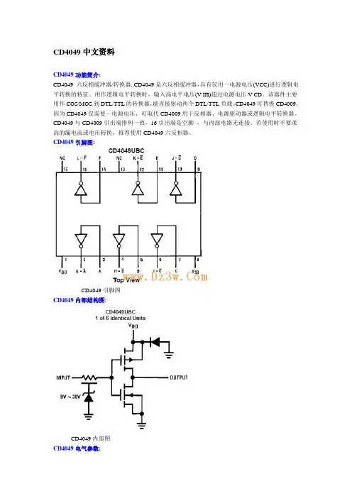
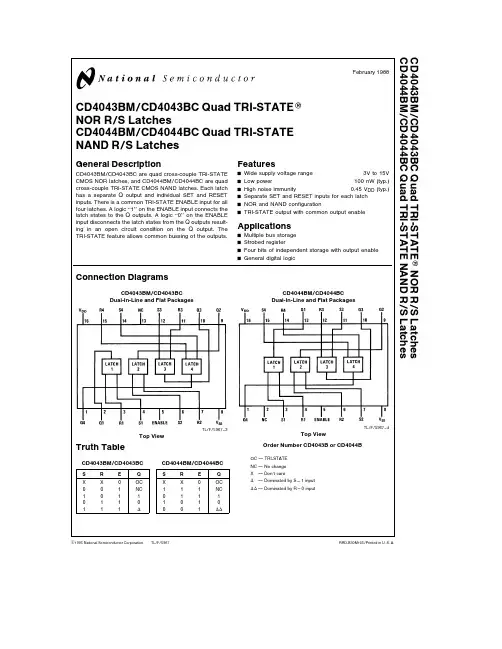
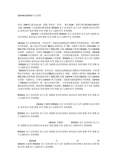
© 2002 Fairchild Semiconductor Corporation DS005971October 1987Revised April 2002CD4049UBC • CD4050BC Hex Inverting Buffer • Hex Non-Inverting BufferCD4049UBC • CD4050BC Hex Inverting Buffer •Hex Non-Inverting BufferGeneral DescriptionThe CD4049UBC and CD4050BC hex buffers are mono-lithic complementary MOS (CMOS) integrated circuits con-structed with N- and P-channel enhancement mode transistors. These devices feature logic level conversion using only one supply voltage (V DD ). The input signal high level (V IH ) can exceed the V DD supply voltage when these devices are used for logic level conversions. These devices are intended for use as hex buffers, CMOS to DTL/TTL converters, or as CMOS current drivers, and at V DD =5.0V, they can drive directly two DTL/TTL loads over the full operating temperature range.Featuress Wide supply voltage range: 3.0V to 15Vs Direct drive to 2 TTL loads at 5.0V over full temperature range s High source and sink current capabilitys Special input protection permits input voltages greater than V DDApplications•CMOS hex inverter/buffer •CMOS to DTL/TTL hex converter •CMOS current “sink” or “source” driver •CMOS HIGH-to-LOW logic level converterOrdering Code:Devices also available in T ape and Reel. Specify by appending the suffix letter “X ” to the ordering code.Connection DiagramsPin Assignments for DIPCD4049UBCTop View CD4050BCTop ViewOrder Number Package NumberPackage DescriptionCD4049UBCM M16A 16-Lead Small Outline Integrated Circuit (SOIC), JEDEC MS-012, 0.150" Narrow CD4049UBCN N16E 16-Lead Plastic Dual-In-Line Package (PDIP), JEDEC MS-001, 0.300" Wide CD4050BCM M16A 16-Lead Small Outline Integrated Circuit (SOIC), JEDEC MS-012, 0.150" Narrow CD4050BCNN16E16-Lead Plastic Dual-In-Line Package (PDIP), JEDEC MS-001, 0.300" Wide 2C D 4049U B C • C D 4050B CSchematic DiagramsCD4049UBC 1 of 6 Identical UnitsCD4050BC1 of 6 Identical UnitsCD4049UBC • CD4050BCAbsolute Maximum Ratings (Note 1)(Note 2)Recommended Operating Conditions (Note 2)Note 1: “Absolute Maximum Ratings ” are those values beyond which the safety of the device cannot be guaranteed; they are not meant to imply that the devices should be operated at these limits. The table of “Recom-mended Operating Conditions ” and “Electrical Characteristics ” provides conditions for actual device operation.Note 2: V SS = 0V unless otherwise specified.DC Electrical Characteristics (Note 3)Note 3: V SS = 0V unless otherwise specified.Supply Voltage (V DD )−0.5V to +18V Input Voltage (V IN )−0.5V to +18V Voltage at Any Output Pin (V OUT )−0.5V to V DD + 0.5V Storage Temperature Range (T S )−65°C to +150°CPower Dissipation (P D )Dual-In-Line 700 mW Small Outline 500 mWLead Temperature (T L )(Soldering, 10 seconds)260°C Supply Voltage (V DD )3V to 15V Input Voltage (V IN )0V to 15V Voltage at Any Output Pin (V OUT )0 to V DDOperating Temperature Range (T A )CD4049UBC, CD4050BC−55°C to +125°CSymbol ParameterConditions−55°C +25°C +125°C UnitsMinMax MinTyp Max MinMax I DDQuiescent Device CurrentV DD = 5V 1.00.01 1.030µAV DD = 10V 2.00.01 2.060V DD = 15V4.00.034.0120V OLLOW Level Output VoltageV IH = V DD , V IL = 0V,|I O | < 1 µA V DD = 5V 0.0500.050.05VV DD = 10V 0.0500.050.05V DD = 15V0.050.050.05V OHHIGH Level Output VoltageV IH = V DD , V IL = 0V,|I O | < 1 µA V DD = 5V 4.95 4.955 4.95VV DD = 10V 9.959.95109.95V DD = 15V14.9514.951514.95V ILLOW Level Input Voltage |I O | < 1 µA(CD4050BC Only)V DD = 5V, V O = 0.5V 1.5 2.25 1.5 1.5V V DD = 10V, V O = 1V 3.0 4.5 3.0 3.0V DD = 15V, V O = 1.5V4.0 6.75 4.0 4.0V ILLOW Level Input Voltage |I O | < 1 µA(CD4049UBC Only)V DD = 5V, V O = 4.5V 1.0 1.5 1.0 1.0V V DD = 10V, V O = 9V 2.0 2.5 2.0 2.0V DD = 15V, V O = 13.5V3.03.53.03.0V IHHIGH Level Input Voltage |I O | < 1 µA(CD4050BC Only)V DD = 5V, V O = 4.5V 3.5 3.5 2.75 3.5V V DD = 10V, V O = 9V 7.07.0 5.57.0V DD = 15V, V O = 13.5V11.011.08.2511.0V IHHIGH Level Input Voltage |I O | < 1 µA(CD4049UBC Only)V DD = 5V, V O = 0.5V 4.0 4.0 3.5 4.0V V DD = 10V, V O = 1V 8.08.07.58.0V DD = 15V, V O = 1.5V12.012.011.512.0I OLLOW Level Output Current V IH = V DD , V IL = 0V (Note 4)V DD = 5V, V O = 0.4V 5.6 4.65 3.2mA V DD = 10V, V O = 0.5V 129.812 6.8V DD = 15V, V O = 1.5V35294020I OHHIGH Level Output Current V IH = V DD , V IL = 0V (Note 4)V DD = 5V, V O = 4.6V −1.3−1.1−1.6−0.72mA V DD = 10V, V O = 9.5V −2.6−2.2−3.6−1.5V DD = 15V, V O = 13.5V−8.0−7.2−12−5I INInput CurrentV DD = 15V, V IN = 0V −0.1−10−5−0.1−1.0µA V DD = 15V, V IN = 15V0.110−50.11.0 4C D 4049U B C • C D 4050B CDC Electrical Characteristics (Continued)Note 4: These are peak output current capabilities. Continuous output current is rated at 12 mA maximum. The output current should not be allowed to exceed this value for extended periods of time. I OL and I OH are tested one output at a time.AC Electrical Characteristics (Note 5)CD4049UBCT A = 25°C, C L = 50 pF, R L = 200k, t r = t f = 20 ns, unless otherwise specifiedNote 5: AC Parameters are guaranteed by DC correlated testing.AC Electrical Characteristics (Note 6)CD4050BCT A = 25°C, C L = 50 pF, R L = 200k, t r = t f = 20 ns, unless otherwise specifiedNote 6: AC Parameters are guaranteed by DC correlated testing.Symbol ParameterConditions Min Typ Max Units t PHLPropagation Delay Time V DD = 5V 3065nsHIGH-to-LOW LevelV DD = 10V 2040V DD = 15V 1530t PLHPropagation Delay Time V DD = 5V 4585nsLOW-to-HIGH LevelV DD = 10V 2545V DD = 15V 2035t THLTransition Time V DD = 5V 3060nsHIGH-to-LOW LevelV DD = 10V 2040V DD = 15V 1530t TLHTransition Time V DD = 5V 60120ns LOW-to-HIGH LevelV DD = 10V 3055V DD = 15V 2545C INInput CapacitanceAny Input1522.5pFSymbol ParameterConditions Min Typ Max Units t PHLPropagation Delay Time V DD = 5V 60110nsHIGH-to-LOW LevelV DD = 10V 2555V DD = 15V 2030t PLHPropagation Delay Time V DD = 5V 60120nsLOW-to-HIGH LevelV DD = 10V 3055V DD = 15V 2545t THLTransition Time V DD = 5V 3060nsHIGH-to-LOW LevelV DD = 10V 2040V DD = 15V 1530t TLHTransition Time V DD = 5V 60120ns LOW-to-HIGH LevelV DD = 10V 3055V DD = 15V 2545C INInput CapacitanceAny Input57.5pFCD4049UBC • CD4050BCSwitching Time WaveformsTypical ApplicationsCMOS to TLL or CMOS at a Lower V DDV DD1 ≥ V DD2In the case of the CD4049UBC the output drive capability increases with increasing input voltage. E.g., If V DD1 = 10V the CD4049UBC could drive 4 TTL loads. 6C D 4049U B C • C D 4050B CPhysical Dimensionsinches (millimeters) unless otherwise noted16-Lead Small Outline Integrated Circuit (SOIC), JEDEC MS-012, 0.150" NarrowPackage Number M16A7CD4049UBC • CD4050BC Hex Inverting Buffer • Hex Non-Inverting BufferPhysical Dimensions inches (millimeters) unless otherwise noted (Continued)16-Lead Plastic Dual-In-Line Package (PDIP), JEDEC MS-001, 0.300" WidePackage Number N16EFairchild does not assume any responsibility for use of any circuitry described, no circuit patent licenses are implied and Fairchild reserves the right at any time without notice to change said circuitry and specifications.LIFE SUPPORT POLICYFAIRCHILD ’S PRODUCTS ARE NOT AUTHORIZED FOR USE AS CRITICAL COMPONENTS IN LIFE SUPPORT DEVICES OR SYSTEMS WITHOUT THE EXPRESS WRITTEN APPROVAL OF THE PRESIDENT OF FAIRCHILD SEMICONDUCTOR CORPORATION. As used herein:1.Life support devices or systems are devices or systems which, (a) are intended for surgical implant into the body, or (b) support or sustain life, and (c) whose failure to perform when properly used in accordance with instructions for use provided in the labeling, can be rea-sonably expected to result in a significant injury to the user.2. A critical component in any component of a life support device or system whose failure to perform can be rea-sonably expected to cause the failure of the life support device or system, or to affect its safety or effectiveness.。