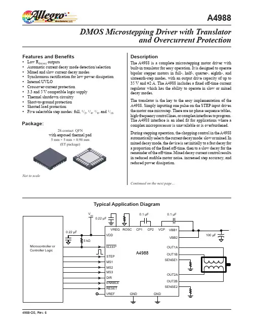
Features and Benefits▪ Low R ds(on) outputs▪ Automatic current decay mode detection/selection ▪ Mixed and slow current decay modes▪ Synchronous rectification for low power dissipation ▪ Internal UVLO▪ Crossover-current protection▪ 3.3 and 5 V compatible logic supply ▪ Thermal shutdown circuitry ▪ Short-to-ground protection ▪ Shorted load protection▪Five selectable step modes: full, 1/2, 1/4, 1/8, and 1/16Package:DescriptionThe A4988 is a complete microstepping motor driver with built-in translator for easy operation. It is designed to operate bipolar stepper motors in full-, half-, quarter-, eighth-, and sixteenth-step modes, with an output drive capacity of up to 35 V and ±2 A. The A4988 includes a fixed off-time current regulator which has the ability to operate in slow or mixed decay modes.The translator is the key to the easy implementation of the A4988. Simply inputting one pulse on the STEP input drives the motor one microstep. There are no phase sequence tables, high-frequency control lines, or complex interfaces to program. The A4988 interface is an ideal fit for applications where a complex microprocessor is unavailable or is overburdened.During stepping operation, the chopping control in the A4988 automatically selects the current decay mode: slow or mixed. In mixed decay mode, the device is set initially to a fast decay for a proportion of the fixed off-time, then to a slow decay for the remainder of the off-time. Mixed decay current control results in reduced audible motor noise, increased step accuracy, and reduced power dissipation.DMOS Microstepping Driver with Translatorand Overcurrent ProtectionContinued on the next page…A498828-contact QFNwith exposed thermal pad5 mm × 5 mm × 0.90 mm(ET package)Typical Application DiagramNot to scaleInternal synchronous rectification control circuitry is provided to improve power dissipation during PWM operation. Internal circuit protection includes: thermal shutdown with hysteresis, undervoltage lockout (UVLO), and crossover-current protection. Special power-on sequencing is not required.The A 4988 is supplied in a surface-mount QFN package (ET), 5 mm × 5 mm, with a nominal overall package height of 0.90 mm and an exposed pad for enhanced thermal dissipation. It is lead (Pb) free (suffix –T), with 100% matte-tin-plated leadframes.Description (continued)Absolute Maximum RatingsCharacteristicSymbol NotesRating Units Load Supply Voltage V BB 35V Output Current I OUT ±2A Logic Input Voltage V IN –0.3 to 5.5V Logic Supply Voltage V DD–0.3 to 5.5V Motor Outputs Voltage –2.0 to 37V Sense Voltage V SENSE –0.5 to 0.5V Reference VoltageV REF 5.5V Operating Ambient Temperature T A Range S–20 to 85ºC Maximum Junction T J (max)150ºC Storage TemperatureT stg–55 to 150ºCSelection GuidePart Number PackagePackingA4988SETTR-T28-contact QFN with exposed thermal pad1500 pieces per 7-in. reelFunctional Block DiagramELECTRICAL CHARACTERISTICS1at T A= 25°C, V BB = 35 V (unless otherwise noted)Characteristics Symbol Test Conditions Min.Typ.2Max.Units Output DriversLoad Supply Voltage Range V BB Operating8–35V During Sleep Mode0–35VLogic Supply Voltage Range V DD Operating3– 5.5VOutput On-Resistance R ds(on)Source driver, I OUT = –1.5 A–320430mΩSink driver, I OUT = 1.5 A–320430mΩBody Diode Forward Voltage V F Source diode, I F = –1.5 A–– 1.2V Sink diode, I F = 1.5 A–– 1.2VMotor Supply Current I BB f PWM < 50 kHz ––4mA Operating, outputs disabled––2mA Sleep Mode––10µALogic Supply Current I DD f PWM < 50 kHz––8mA Outputs off––5mA Sleep Mode––10µAControl LogicLogic Input Voltage V IN(1)V DD × 0.7––V V IN(0)––V DD × 0.3VLogic Input Current I IN(1)V IN = V DD × 0.7–20<1.020µA I IN(0)V IN = V DD × 0.3–20<1.020µAMicrostep Select R MS1MS1 pin–100–kΩR MS2MS2 pin–50–kΩR MS3MS3 pin–100–kΩLogic Input Hysteresis V HYS(IN)As a % of V DD51119% Blank Time t BLANK0.71 1.3μsFixed Off-Time tOFF OSC = VDD or GND203040μs R OSC = 25 kΩ233037μsReference Input Voltage Range V REF0–4V Reference Input Current I REF–303μACurrent Trip-Level Error3err I V REF = 2 V, %I TripMAX = 38.27%––±15% V REF = 2 V, %I TripMAX= 70.71%––±5% V REF = 2 V, %I TripMAX= 100.00%––±5%Crossover Dead Time t DT100475800ns ProtectionOvercurrent Protection Threshold4I OCPST 2.1––A Thermal Shutdown Temperature T TSD–165–°C Thermal Shutdown Hysteresis T TSDHYS–15–°C VDD Undervoltage Lockout V DDUVLO V DD rising 2.7 2.8 2.9V VDD Undervoltage Hysteresis V DDUVLOHYS–90–mV1 For input and output current specifications, negative current is defined as coming out of (sourcing) the specified device pin.2 Typical data are for initial design estimations only, and assume optimum manufacturing and application conditions. Performance may vary for individual units, within the specified maximum and minimum limits.3 V ERR = [(V REF/8) – V SENSE] / (V REF/8).4 Overcurrent protection (OCP) is tested at T A = 25°C in a restricted range and guaranteed by characterization.THERMAL CHARACTERISTICSCharacteristicSymbol Test Conditions*Value Units Package Thermal ResistanceR θJAFour-layer PCB, based on JEDEC standard32ºC/W*Additional thermal information available on Allegro website.Temperature, T A (°C)P o w e r D i s s i p a t i o n , P D (W )0.501.502.002.503.003.504.001.0020406080100120140160Power Dissipation versus Ambient TemperatureFigure 1: Logic Interface Timing DiagramMS1, MS2, MS3, Table 1: Microstepping Resolution Truth TableTime DurationSymbol Typ.Unit STEP minimum, HIGH pulse width t A 1μs STEP minimum, LOW pulse width t B 1μs Setup time, input change to STEP t C 200ns Hold time, input change to STEPt D200nsMS1MS2 MS3 Microstep Resolution Excitation Mode L L L Full Step 2 Phase H L L Half Step 1-2 Phase L H L Quarter Step W1-2 Phase H H L Eighth Step 2W1-2 Phase HHHSixteenth Step4W1-2 PhaseDevice Operation. The A4988 is a complete microstepping motor driver with a built-in translator for easy operation with minimal control lines. It is designed to operate bipolar stepper motors in full-, half-, quarter-, eighth, and sixteenth-step modes. The currents in each of the two output full-bridges and all of the N-channel DMOS FETs are regulated with fixed off-time PWM (pulse-width modulated) control circuitry. At each step, the cur-rent for each full-bridge is set by the value of its external current-sense resistor (R S1 and R S2), a reference voltage (V REF), and the output voltage of its DAC (which in turn is controlled by the output of the translator).At power-on or reset, the translator sets the DACs and the phase current polarity to the initial Home state (shown in Figures 9 through 13), and the current regulator to Mixed decay mode for both phases. When a step command signal occurs on the STEP input, the translator automatically sequences the DACs to the next level and current polarity. (See Table 2 for the current-level sequence.) The microstep resolution is set by the combined effect of the MSx inputs, as shown in Table 1.When stepping, if the new output levels of the DACs are lower than their previous output levels, then the decay mode for the active full-bridge is set to Mixed. If the new output levels of the DACs are higher than or equal to their previous levels, then the decay mode for the active full-bridge is set to Slow. This auto-matic current decay selection improves microstepping perfor-mance by reducing the distortion of the current waveform that results from the back EMF of the motor.Microstep Select (MSx). The microstep resolution is set by the voltage on logic inputs MSx, as shown in Table 1. The MS1 and MS3 pins have a 100 kΩ pull-down resistance, and the MS2 pin has a 50 kΩ pull-down resistance. When changing the step mode, the change does not take effect until the next STEP rising edge.If the step mode is changed without a translator reset, and abso-lute position must be maintained, it is important to change the step mode at a step position that is common to both step modes in order to avoid missing steps. When the device is powered down, or reset due to TSD or an overcurrent event, the translator is set to the home position which is by default common to all step modes.Mixed Decay Operation. The bridge operates in Mixed decay mode, at power-on and reset, and during normal running according to the ROSC configuration and the step sequence, as shown in Figures 9 through 13. During Mixed decay mode, when the trip point is reached, the A4988 initially goes into a fast decay interval for 31.25% of the off-time, t OFF . After that, it switchesto slow decay for the remainder of t OFF. A timing diagram for this feature appears on the next page.Typically, mixed decay is only necessary when the current in the winding is going from a higher value to a lower value as determined by the state of the translator. For most loads, automatically selected mixed decay is convenient because it minimizes ripple when the current is rising and prevents missed steps when the current is falling. For some applications where microstepping at very low speeds is necessary, the lack of back EMF in the winding causes the current to increase in the load quickly, resulting in missed steps. This is shown in Figure 2. By pulling the ROSC pin to ground, mixed decay is set to be active 100% of the time, for both rising and falling currents, and prevents missed steps as shown in Figure 3. If this is not an issue, it is recommended that automatically selected mixed decay be used, because it will produce reduced ripple currents. Refer to the Fixed Off-Time section for details.Low Current Microstepping. Intended for applications where the minimum on-time prevents the output current from regulating to the programmed current level at low current steps. To prevent this, the device can be set to operate in Mixed decay mode on both rising and falling portions of the current waveform. This feature is implemented by shorting the ROSC pin to ground. In this state, the off-time is internally set to 30 µs.Reset Input (¯R¯¯E¯¯S¯¯E¯¯T¯ ). The ¯R¯ ¯E¯ ¯S ¯E¯ ¯T¯ input sets the translator to a predefined Home state (shown in Figures 9 through 13), and turns off all of the FET outputs. All STEP inputs are ignored until the ¯R¯ ¯E¯ ¯S ¯E¯ ¯T¯ input is set to high.Step Input (STEP). A low-to-high transition on the STEP input sequences the translator and advances the motor one incre-ment. The translator controls the input to the DACs and the direc-Functional DescriptionFigure 2: Missed Steps in Low-Speed MicrosteppingFigure 3: Continuous Stepping Using Automatically-Selected Mixed Stepping (ROSC pin grounded)t → , 1 s/div.Step input 10 V/div.Mixed Decay No Missed StepsI LOAD 500 mA/div.t → , 1 s/div.Step input 10 V/div.Slow DecaySlow DecaySlow DecaySlow DecayMixed DecayMixed DecayMixed DecayMixed DecayMissed StepVoltage on ROSC terminal 2 V/div.tion of current flow in each winding. The size of the increment is determined by the combined state of the MSx inputs. Direction Input (DIR).This determines the direction of rota-tion of the motor. Changes to this input do not take effect until the next STEP rising edge.Internal PWM Current Control. Each full-bridge is con-trolled by a fixed off-time PWM current control circuit that limits the load current to a desired value, I TRIP . Initially, a diagonal pair of source and sink FET outputs are enabled and current flows through the motor winding and the current sense resistor, R S x. When the voltage across R S x equals the DAC output voltage, the current sense comparator resets the PWM latch. The latch then turns off the appropriate source driver and initiates a fixed off-time decay modeThe maximum value of current limiting is set by the selection of R S x and the voltage at the VREF pin. The transconductance func-tion is approximated by the maximum value of current limiting, I TripMAX (A), which is set byI TripMAX = V REF / ( 8 × R S)where R S is the resistance of the sense resistor (Ω) and V REF is the input voltage on the REF pin (V).The DAC output reduces the V REF output to the current sense comparator in precise steps, such thatI trip = (%I TripMAX / 100)× I TripMAX(See Table 2 for %I TripMAX at each step.)It is critical that the maximum rating (0.5 V) on the SENSE1 and SENSE2 pins is not exceeded.Fixed Off-Time. The internal PWM current control circuitry uses a one-shot circuit to control the duration of time that the DMOS FETs remain off. The off-time, t OFF, is determined by the ROSC terminal. The ROSC terminal has three settings:▪ ROSC tied to VDD — off-time internally set to 30 µs; decay mode is automatic Mixed, except when in full-step where decay mode is set to Slow.▪ ROSC tied directly to ground — off-time internally set to30 µs; current decay is set to Mixed for both increasing and decreasing currents for all step modes.▪ ROSC through a resistor to ground — off-time is determined by the following formula; the decay mode is automatic Mixed for all step modes except full-step which is set to Slow.t OFF ≈ R OSC⁄ 825where t OFF is in µs.Blanking. This function blanks the output of the current sense comparators when the outputs are switched by the internal current control circuitry. The comparator outputs are blanked to prevent false overcurrent detection due to reverse recovery currents of the clamp diodes, and switching transients related to the capacitance of the load. The blank time, t BLANK (µs), is approximatelyt BLANK≈ 1 µsShorted Load and Short-to-Ground Protection.If the motor leads are shorted together, or if one of the leads is shorted to ground, the driver will protect itself by sensing the overcurrent event and disabling the driver that is shorted, protect-ing the device from damage. In the case of a short-to-ground, the device will remain disabled (latched) until the S¯ ¯L¯ ¯E¯ ¯E¯ ¯P input goes high or V DD power is removed. A short-to-ground overcurrent event is shown in Figure 4.When the two outputs are shorted together, the current path is through the sense resistor. After the blanking time (≈1 µs) expires, the sense resistor voltage is exceeding its trip value, due to the overcurrent condition that exists. This causes the driver to go into a fixed off-time cycle. After the fixed off-time expires, the driver turns on again and the process repeats. In this condition, the driver is completely protected against overcurrent events, but the short is repetitive with a period equal to the fixed off-time of the driver. This condition is shown in Figure 5.During a shorted load event, it is normal to observe both a posi-tive and negative current spike as shown in Figure 3, due to the direction change implemented by the Mixed decay feature. This is shown in Figure 6. In both instances, the overcurrent circuitry is protecting the driver and prevents damage to the device. Charge Pump (CP1 and CP2). The charge pump is usedto generate a gate supply greater than that of V BB for driving the source-side FET gates. A 0.1 µF ceramic capacitor should be connected between CP1 and CP2. In addition, a 0.1 µF ceramic capacitor is required between VCP and VBB, to act as a reservoir for operating the high-side FET gates.Capacitor values should be Class 2 dielectric ±15% maximum, or tolerance R, according to EIA (Electronic Industries Alliance) specifications.V REG(VREG). This internally generated voltage is used to operate the sink-side FET outputs. The nominal output voltage of the VREG terminal is 7 V. The VREG pin must be decoupled with a 0.22 µF ceramic capacitor to ground. V REG is internally monitored. In the case of a fault condition, the FET outputs of the A4988 are disabled.Capacitor values should be Class 2 dielectric ±15% maximum, or tolerance R, according to EIA (Electronic Industries Alliance) specifications.Enable Input (¯E¯¯N¯¯A¯¯B¯¯L¯¯E¯). This input turns on or off all of the FET outputs. When set to a logic high, the outputs are disabled. When set to a logic low, the internal control enables the outputs as required. The translator inputs STEP, DIR, and MSx, as well as the internal sequencing logic, all remain active, independent of the ¯E¯ ¯N¯ ¯A¯ ¯B¯ ¯L¯ ¯E¯ input state.Shutdown. In the event of a fault, overtemperature (excess T J) or an undervoltage (on VCP), the FET outputs of the A4988 are disabled until the fault condition is removed. At power-on, the UVLO (undervoltage lockout) circuit disables the FET outputs and resets the translator to the Home state.Sleep Mode (¯S¯¯L¯¯E¯¯E¯¯P¯). To minimize power consumption when the motor is not in use, this input disables much of the internal circuitry including the output FETs, current regulator, and charge pump. A logic low on the S¯ ¯L¯ ¯E¯ ¯E¯ ¯P pin puts the A4988 into Sleep mode. A logic high allows normal operation, as wellas startup (at which time the A4988 drives the motor to the Home microstep position). When emerging from Sleep mode, in order to allow the charge pump to stabilize, provide a delay of 1 ms before issuing a Step command.Mixed Decay Operation. The bridge operates in Mixed decay mode, depending on the step sequence, as shown in Fig-ures 9 through 13. As the trip point is reached, the A4988 initially goes into a fast decay interval for 31.25% of the off-time, t OFF. After that, it switches to slow decay for the remainder of t OFF. A timing diagram for this feature appears in Figure 7.Synchronous Rectification. When a PWM-off cycle is triggered by an internal fixed-off time cycle, load current recircu-lates according to the decay mode selected by the control logic. This synchronous rectification feature turns on the appropriate FETs during current decay, and effectively shorts out the body diodes with the low FET R ds(on). This reduces power dissipation significantly, and can eliminate the need for external Schottky diodes in many applications. Synchronous rectification turns off when the load current approaches zero (0 A), preventing reversal of the load current.t →Fixed off-time5 A / div.t →5 A / div.Figure 4: Short-to-Ground EventFigure 5. Shorted Load (OUTxA → OUTxB) in Slow Decay Mode Figure 6: Shorted Load (OUTxA → OUTxB) in Mixed Decay ModeFixed off-timeFast decay portion(direction change)t →5 A / div.FaultlatchedV STEPI OUTI OUTtEnlargement A70.71–70.710100.00–100.00Symbol Characteristict off Device fixed off-time I PEAK Maximum output current t SD Slow decay interval t FD Fast decay interval I OUTDevice output currentFigure 7: Current Decay Modes Timing ChartApplication LayoutLayout. The printed circuit board should use a heavy ground-plane. For optimum electrical and thermal performance, theA4988 must be soldered directly onto the board. Pins 3 and 18 are internally fused, which provides a path for enhanced thermal dissipation. Theses pins should be soldered directly to an exposed surface on the PCB that connects to thermal vias are used to transfer heat to other layers of the PCB.In order to minimize the effects of ground bounce and offset issues, it is important to have a low-impedance single-point ground, known as a star ground, located very close to the device. By making the connection between the pad and the ground plane directly under the A4988, that area becomes an ideal location for a star ground point. A low-impedance ground will prevent ground bounce during high-current operation and ensure that the supply voltage remains stable at the input terminal.The two input capacitors should be placed in parallel, and as close to the device supply pins as possible. The ceramic capaci-tor (CIN1) should be closer to the pins than the bulk capacitor (CIN2). This is necessary because the ceramic capacitor will be responsible for delivering the high-frequency current components. The sense resistors, RSx , should have a very low-impedance path to ground, because they must carry a large current while supporting very accurate voltage measurements by the current sense comparators. Long ground traces will cause additional voltage drops, adversely affecting the ability of the comparators to accurately measure the current in the windings. The SENSEx pins have very short traces to the RSx resistors and very thick, low-impedance traces directly to the star ground under the device. If possible, there should be no other components on the sense circuits.Figure 8: Typical Application and Circuit LayoutPin Circuit DiagramsFigure 10: Decay Modes for Half-Step IncrementsFigure 9: Decay Mode for Full-Step IncrementsPhase 2I OUT2ADirection = H(%)Phase 1I OUT1ADirection = H(%)STEPRESETPhase 2I OUT2BDirection = H(%)Phase 1I OUT1ADirection = H(%)STEPPhase 2I OUT2BDirection = H(%)Phase 1I OUT1ADirection = H(%)STEPFigure 11: Decay Modes for Quarter-Step IncrementsDIR= HDIR= HDIR= HFigure 12: Decay Modes for Eighth-Step IncrementsPhase 2I OUT2BDirection = H(%)Phase 1I OUT1ADirection = H(%)STEPDIR= HFigure 13: Decay Modes for Sixteenth-Step IncrementsPhase 2I OUT2BDirection = H(%)Phase 1I OUT1ADirection = H(%)STEPDIR= HTable 2: Step Sequencing SettingsHome microstep position at Step Angle 45º; DIR = HPinout DiagramTerminal List TableName NumberDescriptionCP14Charge pump capacitor terminal CP25Charge pump capacitor terminal VCP 6Reservoir capacitor terminal VREG 8Regulator decoupling terminal MS19Logic input MS210Logic input MS311Logic input ¯R ¯ ¯E ¯ ¯S ¯ ¯E ¯ ¯T ¯ 12Logic input ROSC 13Timing set ¯S ¯ ¯L ¯ ¯E ¯ ¯E ¯ ¯P ¯ 14Logic input VDD 15Logic supply STEP 16Logic inputREF 17G m reference voltage input GND 3, 18Ground*DIR 19Logic inputOUT1B 21DMOS Full Bridge 1 Output B VBB122Load supplySENSE123Sense resistor terminal for Bridge 1OUT1A 24DMOS Full Bridge 1 Output A OUT2A 26DMOS Full Bridge 2 Output A SENSE227Sense resistor terminal for Bridge 2VBB228Load supplyOUT2B 1DMOS Full Bridge 2 Output B ¯E ¯ ¯N ¯ ¯A ¯ ¯B ¯ ¯L ¯ ¯E ¯ 2Logic input NC 7, 20, 25No connectionPAD–Exposed pad for enhanced thermal dissipation**The GND pins must be tied together externally by connecting to the PAD ground plane under the device.B B 2E N S E 2U T 2ACU T 1AE N S E 1B B 1OUT1B NC DIRGND REF STEP VDDET Package, 28-Pin QFN with Exposed Thermal PadA Terminal #1 mark areaB Exposed thermal pad (reference only, terminal #1 identifier appearance at supplier discretion)For Reference Only; not for tooling use (reference JEDEC MO-220VHHD-1)Dimensions in millimetersExact case and lead configuration at supplier discretion within limits shownC Reference land pattern layout (reference IPC7351 QFN50P500X500X100-29V1M);All pads a minimum of 0.20 mm from all adjacent pads; adjust as necessary to meet application process requirements and PCB layout tolerances; when mounting on a multilayer PCB, thermal vias at the exposed thermal pad land can improve thermal dissipation (reference EIA/JEDEC Standard JESD51-5)PCB Layout Reference View0.73 MAX1.15CD Coplanarity includes exposed thermal pad and terminalsFor the latest version of this document, visit our website:Revision HistoryRevisionRevision Date Description of Revision4January 27, 2012Updated I OCPST5May 7, 2014Revised text on page 9; revised Figure 8 and Table 26January 14, 2016Updated VBB, IBB, and IDD in Electrical Characteristics tableCopyright ©2016, Allegro MicroSystems, LLCAllegro MicroSystems, LLC reserves the right to make, from time to time, such departures from the detail specifications as may be required topermit improvements in the performance, reliability, or manufacturability of its products. Before placing an order, the user is cautioned to verify that the information being relied upon is current.Allegro’s products are not to be used in any devices or systems, including but not limited to life support devices or systems, in which a failure of Allegro’s product can reasonably be expected to cause bodily harm.use; nor for any infringement of patents or other rights of third parties which may result from its use.。