半导体照明术语对照表
- 格式:docx
- 大小:73.76 KB
- 文档页数:35
外延术语1、外延生长(Epitaxy)2、量子阱(Quantum Well)3、能带工程(Energyband engineering)4、半导体发光二极管(Light Emitting Diode)5、PN结的击穿(PN junction Striking)6 Deposition)7、异质结构(Heterogeneous Structure)8、量子阱半导体激光器(Quantum Well Laser)9、超晶格(Super Lattice)EpitaxyGaP:磷化镓n-GaN:N型氮化镓p-GaN:P型氮化镓GaAs:砷化镓GaN:氮化镓AlInGaP:磷化铝镓铟(铝铟镓磷)AlGaAs:砷化铝镓(铝镓砷)InGaN 铟镓氮AlGaN 铝镓氮Wafer:晶片、外延片分析仪器1、XRD:X射线衍射仪,主peak GaN分析仪器2、PL:荧光光谱仪(或光致发光光谱仪),Peak强度越强,FWHM越窄,表示有较佳的QW。
3、Hall:霍尔测试仪,利用霍尔效应测量载流子(对n-GaN载流子为电子,对p-GaN,载流子为空穴)迁移率(mobility)以及Sheet Resistance,分析时同结构若有相同的掺杂(Doping),若是量测的迁移率mobility较小,可以推测此结构有较多的缺陷(Defects)。
4、SEM(Scanning Electron Microscopy):扫描式电子显微镜,测量刻蚀深度、及刻蚀截面状况。
5、Microscope:显微镜6、Differential Microscopy(Nikon-OPTI PHOT):晶相(金相)显微镜,用morphology)。
7、EDS EDS之仪器构造主要是由一个硅(锂)固态侦测器为核心,它是由硅单晶参杂锂原子而成的。
8、:金属有机化学汽相9、TEM10、SIMS:二次离子质谱仪,测量每层的掺杂状况,可测量P-GaN以及N-GaN的掺杂状况,以及掺杂载子的浓度以及扩散距离等测量。
半导体一些术语的中英文对照离子注入机 ion implanterLSS理论 Lindhand Scharff and Schiott theory 又称“林汉德-斯卡夫-斯高特理论”。
沟道效应 channeling effect射程分布 range distribution深度分布 depth distribution投影射程 projected range阻止距离 stopping distance阻止本领 stopping power标准阻止截面 standard stopping cross section退火 annealing激活能 activation energy等温退火 isothermal annealing激光退火 laser annealing应力感生缺陷 stress-induced defect择优取向 preferred orientation制版工艺 mask-making technology图形畸变 pattern distortion初缩 first minification精缩 final minification母版 master mask铬版 chromium plate干版 dry plate乳胶版 emulsion plate透明版 see-through plate高分辨率版 high resolution plate, HRP超微粒干版 plate for ultra-microminiaturization 掩模 mask掩模对准 mask alignment对准精度 alignment precision光刻胶 photoresist又称“光致抗蚀剂”。
负性光刻胶 negative photoresist正性光刻胶 positive photoresist无机光刻胶 inorganic resist多层光刻胶 multilevel resist电子束光刻胶 electron beam resistX射线光刻胶 X-ray resist刷洗 scrubbing甩胶 spinning涂胶 photoresist coating后烘 postbaking光刻 photolithographyX射线光刻 X-ray lithography电子束光刻 electron beam lithography离子束光刻 ion beam lithography深紫外光刻 deep-UV lithography光刻机 mask aligner投影光刻机 projection mask aligner曝光 exposure接触式曝光法 contact exposure method接近式曝光法 proximity exposure method光学投影曝光法 optical projection exposure method 电子束曝光系统 electron beam exposure system分步重复系统 step-and-repeat system显影 development线宽 linewidth去胶 stripping of photoresist氧化去胶 removing of photoresist by oxidation等离子[体]去胶 removing of photoresist by plasma 刻蚀 etching干法刻蚀 dry etching反应离子刻蚀 reactive ion etching, RIE各向同性刻蚀 isotropic etching各向异性刻蚀 anisotropic etching反应溅射刻蚀 reactive sputter etching离子铣 ion beam milling又称“离子磨削”。
外延术语1、外延生长(Epitaxy)2、量子阱(Quantum Well)3、能带工程(Energyband engineering)4、半导体发光二极管(Light Emitting Diode)5、PN结的击穿(PN junction Striking)6 Deposition)7、异质结构(Heterogeneous Structure)8、量子阱半导体激光器(Quantum Well Laser)9、超晶格(Super Lattice)EpitaxyGaP:磷化镓n-GaN:N型氮化镓p-GaN:P型氮化镓GaAs:砷化镓GaN:氮化镓AlInGaP:磷化铝镓铟(铝铟镓磷)AlGaAs:砷化铝镓(铝镓砷)InGaN 铟镓氮AlGaN 铝镓氮Wafer:晶片、外延片分析仪器1、XRD:X射线衍射仪,主peak GaN分析仪器2、PL:荧光光谱仪(或光致发光光谱仪),Peak强度越强,FWHM越窄,表示有较佳的QW。
3、Hall:霍尔测试仪,利用霍尔效应测量载流子(对n-GaN载流子为电子,对p-GaN,载流子为空穴)迁移率(mobility)以及Sheet Resistance,分析时同结构若有相同的掺杂(Doping),若是量测的迁移率mobility较小,可以推测此结构有较多的缺陷(Defects)。
4、SEM(Scanning Electron Microscopy):扫描式电子显微镜,测量刻蚀深度、及刻蚀截面状况。
5、Microscope:显微镜6、Differential Microscopy(Nikon-OPTI PHOT):晶相(金相)显微镜,用morphology)。
7、EDS EDS之仪器构造主要是由一个硅(锂)固态侦测器为核心,它是由硅单晶参杂锂原子而成的。
8、:金属有机化学汽相9、TEM10、SIMS:二次离子质谱仪,测量每层的掺杂状况,可测量P-GaN以及N-GaN的掺杂状况,以及掺杂载子的浓度以及扩散距离等测量。
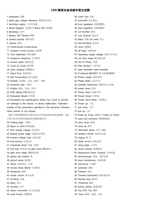
LED照明专业术语中英文对照1 backplane 背板2 Band gap voltage reference 带隙电压参考3 benchtop supply 工作台电源4 Block Diagram 方块图5 Bode Plot 波特图6 Bootstrap 自举7 Bottom FET Bottom FET8 bucket capcitor 桶形电容9 chassis 机架10 Combi-sense Combi-sense11 constant current source 恒流源12 Core Sataration 铁芯饱和13 crossover frequency 交叉频率14 current ripple 纹波电流15 Cycle by Cycle 逐周期16 cycle skipping 周期跳步17 Dead Time 死区时间18 DIE Temperature 核心温度19 Disable 非使能,无效,禁用,关断20 dominant pole 主极点21 Enable 使能,有效,启用22 ESD Rating ESD额定值23 Evaluation Board 评估板24 Exceeding the specifications below may result in perman ent damage to the device, or device malfunction. Operation outside of the parameters specified in the Electrical Characte ristics section is not implied.超过下面的规格使用可能引起永久的设备损害或设备故障。
建议不要工作在电特性表规定的参数范围以外。
25 Failling edge 下降沿26 figure of merit 品质因数27 float charge voltage 浮充电压28 flyback power stage 反驰式功率级29 forward voltage drop 前向压降30 free-running 自由运行31 Freewheel diode 续流二极管32 Full load 满负载33 gate drive 栅极驱动34 gate drive stage 栅极驱动级35 gerber plot Gerber 图36 ground plane 接地层37 Henry 电感单位:亨利38 Human Body Model 人体模式39 Hysteresis 滞回40 inrush current 涌入电流41 Inverting 反相42 jittery 抖动43 Junction 结点44 Kelvin connection 开尔文连接45 Lead Frame 引脚框架46 Lead Free 无铅47 level-shift 电平移动48 Line regulation 电源调整率49 load regulation 负载调整率50 Lot Number 批号51 Low Dropout 低压差52 Miller 密勒53 node 节点54 Non-Inverting 非反相55 novel 新颖的56 off state 关断状态57 Operating supply voltage 电源工作电压58 out drive stage 输出驱动级59 Out of Phase 异相60 Part Number 产品型号61 pass transistor pass transistor62 P-channel MOSFET P沟道MOSFET63 Phase margin 相位裕度64 Phase Node 开关节点65 portable electronics 便携式电子设备66 power down 掉电67 Power Good 电源正常68 Power Groud 功率地69 Power Save Mode 节电模式70 Power up 上电71 pull down 下拉72 pull up 上拉73 Pulse by Pulse 逐脉冲(Pulse by Pulse)74 push pull converter 推挽转换器75 ramp down 斜降76 ramp up 斜升77 redundant diode 冗余二极管78 resistive divider 电阻分压器79 ringing 振铃80 ripple current 纹波电流81 rising edge 上升沿82 sense resistor 检测电阻83 Sequenced Power Supplys 序列电源84 shoot-through 直通,同时导通85 stray inductances. 杂散电感86 sub-circuit 子电路87 substrate 基板88 Telecom 电信89 Thermal Information 热性能信息90 thermal slug 散热片91 Threshold 阈值92 timing resistor 振荡电阻93 Top FET Top FET94 Trace 线路,走线,引线95 Transfer function 传递函数96 Trip Point 跳变点97 turns ratio 匝数比,=Np / Ns。
外延术语1、外延生长〔Epitaxy〕2、量子阱〔Quantum Well〕3、能带工程〔Energyband engineering〕4、半导体发光二极管〔Light Emitting Diode〕5、PN 结的击穿〔PN junction Striking〕6 、金属有机化学汽相沉淀积〔Metal Organic Chemical Vapor Deposition〕7、异质构造〔Heterogeneous Structure〕8、量子阱半导体激光器〔Quantum Well Laser〕9、超晶格〔Super Lattice〕InGaN AlGaN 铟镓氮 铝镓氮3、Hall :霍尔测试仪,利用霍尔效应测量载流子〔对 n-GaN 载流子为电子,对p-GaN,载流子为空穴〕迁移率〔mobility 〕以及 Sheet Resistance ,分析时同构造假设有一样的掺杂〔Doping 〕,假设是量测的迁移率 mobility 较小,可以推想此构造有较多的缺陷〔Defects 〕。
Epitaxy :外延制程〔垒晶〕GaP :磷化镓n-GaN :N 型氮化镓p-GaN :P 型氮化镓GaAs :砷化镓GaN :氮化镓AlInGaP :磷化铝镓铟〔铝铟镓磷〕 AlGaAs :砷化铝镓〔铝镓砷〕Wafer :晶片、外延片器1、XRD :X 射线衍射仪,主 peak GaN 器2、PL :荧光光谱仪〔或光致发光光谱仪〕,Peak 强度越强,FWHM 越窄,表示有较佳的 QW 。
4、SEM 〔Scanning Electron Microscopy 〕:扫描式电子显微镜,测量刻蚀深度、及刻蚀截面状况。
5、Microscope :显微镜6、Differential Microscopy 〔Nikon-OPTI PHOT 〕:晶相〔金相〕显微镜,用以观测磊芯片外表的型态〔morphology 〕。
7、EDS :能量分色散光谱仪,EDS 之仪器构造主要是由一个硅(锂)固态侦测器为核心,它是由硅单晶参杂锂原子而成的。
1 backplane 背板2 Band gap voltage reference 带隙电压参考3 benchtop supply 工作台电源4 Block Diagram 方块图5 Bode Plot 波特图6 Bootstrap 自举7 Bottom FET Bottom FET8 bucket capcitor 桶形电容9 chassis 机架10 Combi-sense Combi-sense11 constant current source 恒流源12 Core Sataration 铁芯饱和13 crossover frequency 交叉频率14 current ripple 纹波电流15 Cycle by Cycle 逐周期16 cycle skipping 周期跳步17 Dead Time 死区时间18 DIE Temperature 核心温度19 Disable 非使能,无效,禁用,关断20 dominant pole 主极点21 Enable 使能,有效,启用22 ESD Rating ESD额定值23 Evaluation Board 评估板24 Exceeding the specifications below may result in permanent damage to the device, or device malfunction. Operation outside of the parameters specified in the Electrical Characteristics section is not implied.超过下面的规格使用可能引起永久的设备损害或设备故障。
建议不要工作在电特性表规定的参数范围以外。
25 Failling edge 下降沿26 figure of merit 品质因数27 float charge voltage 浮充电压28 flyback power stage 反驰式功率级29 forward voltage drop 前向压降30 free-running 自由运行31 Freewheel diode 续流二极管32 Full load 满负载33 gate drive 栅极驱动34 gate drive stage 栅极驱动级35 gerber plot Gerber 图36 ground plane 接地层37 Henry 电感单位:亨利38 Human Body Model 人体模式39 Hysteresis 滞回40 inrush current 涌入电流41 Inverting 反相42 jittery 抖动43 Junction 结点44 Kelvin connection 开尔文连接45 Lead Frame 引脚框架46 Lead Free 无铅47 level-shift 电平移动48 Line regulation 电源调整率49 load regulation 负载调整率50 Lot Number 批号51 Low Dropout 低压差52 Miller 密勒53 node 节点54 Non-Inverting 非反相55 novel 新颖的56 off state 关断状态57 Operating supply voltage 电源工作电压58 out drive stage 输出驱动级59 Out of Phase 异相60 Part Number 产品型号61 pass transistor pass transistor62 P-channel MOSFET P沟道MOSFET63 Phase margin 相位裕度64 Phase Node 开关节点65 portable electronics 便携式电子设备66 power down 掉电67 Power Good 电源正常68 Power Groud 功率地69 Power Save Mode 节电模式70 Power up 上电71 pull down 下拉72 pull up 上拉73 Pulse by Pulse 逐脉冲(Pulse by Pulse)74 push pull converter 推挽转换器75 ramp down 斜降76 ramp up 斜升77 redundant diode 冗余二极管78 resistive divider 电阻分压器79 ringing 振铃80 ripple current 纹波电流81 rising edge 上升沿82 sense resistor 检测电阻83 Sequenced Power Supplys 序列电源84 shoot-through 直通,同时导通85 stray inductances. 杂散电感86 sub-circuit 子电路87 substrate 基板88 Telecom 电信89 Thermal Information 热性能信息90 thermal slug 散热片91 Threshold 阈值92 timing resistor 振荡电阻93 Top FET Top FET94 Trace 线路,走线,引线95 Transfer function 传递函数96 Trip Point 跳变点97 turns ratio 匝数比,=Np / Ns。
半导体照明术语对照表2009年2月«X*XfrMAE *«rvu SWcmtuCTOT «!i血s«acorducTox4evlce AiNlflU 处y (Fwu.】«n(Mmcondi»ri€r) dZ(主& H1-01 "二UD litht-tvitfinc 41«4e FMUUMM.W «f«< fttMtt1 WTVH ■■•■1-C5 MA««I solid «1«te iichtim・•发危«n <10)・iWAit(a> , • CUD) Wft*5伯列■"八Ja»»«w1-06 TV侔#Mfl xaiccokKtarli«h?Lng〔用g件为Ft4的创•山式@・ii£咽1-C W«•ub«Tr«ie m i nsMiR. r«. ArnAWfi^ i z ・ rrin***«n・S«iy 4 Kit epiiaiial wafern.SA出l-w li<ht-r»qttirwdiode ddr R<(WW>iA*・庄黄电«(•・屯口可miftt的什#侔“八*弋找■易1-10 ⑼缺LZD scxlde »h*t或事个戏兄•・功电i»・a.-LED««1-12 Lawn LB> 4Ltcrett*watf hUD4LDMft*«r 兀霑 &・n« NPtt悴彳■氏・1-13 imer 9102efficiency «卫KP生tn尤o厮注入f Y穴It«z比.1-14 mt ft* lltM Erwrtiomefficiency amtotAKwt tutt.出栈C1-15 i-A<* Injection•ffieiwncyft ALDlMl ; -'?/;«IBSH Xfi«<(n电il入如“tx «JK1*1S f outer wrr・ a M«int i B sn 人ux» nt 卜々>;ftBZUu Wf"人・♦代•《!,二血刚g ^ecu>1UMUl・y Mtenia 育■包set・*LH>2<Q ll<UZ fitLB)2*43 DHAtn ・3VLB CUd IrrllM z. g GfM ・«H刈.tR t YAflM^r«ia ❺g.TfitfW l皿g •ugSKLXD —g US 1金电・4W・b・441 i1,■"2 l*l>g 卜“l»lc* LB gut ! :IW > 14M U E“ft ■•|4^XIXDX»U・LD p<we» Lil Inmia^ JKMLUUMUL «wX LBBHYg LBUtB LCD dkw-«w etqur»Mi B /・ nstMvaisHM ito MiZ ・”・auiMWW^BWUD •nrMW0»・Q・3. *■<TB»g创代・• <<n<5jy<w^A«<mtiK I'MHMrt1 Z・ A HMM・ WMaWtfi 位歼■1 TK(4H<ftQ4^«h^AHM.#<-u«/a *»wrtta wU/•►«<•** nHavre^ar-WWtMAIM ・■ P><D e ■ fwa«m «・"♦H ■Uti-wrM —II炖irMCiMUTA创Mh ■r©mal evtaderiwv«cv£ «W<r・*••!< ・K 祁1%•■”^•4BR・2 ・*<r lw“A斡.tl«0U ? • a»• ■X・Rlft«1*f)IBVHH2W1 K6 111 •»hmM€WWH»WtK・ KM feKH >.l ・“IL£lijU・»・fMfQrflrti^ ■*■♦鬲・・tU ・BanXT HIM hrtvrttravM•iriK^tFTfiR0dA<mr.mht VMKM«Ar)■■EK". rx・・«••>NAM tiflBl*ae*er»M^««OlR* < 1 V>«KHS<r)・0 • Hi> MABAftdMT tWMM* H■■刑・・*TBw iCtfMl sdW AAK1 K・・ 4JWU«IF)/ie. d UH ■■ »LB«■・ <ze>・41 n«>i0tai*9«a*. <UH.?><^A ttAU I 水*9r)代卅・・■•rmi•-CB IdlMI 6 etaui R4IMWIWAf・■"•Utlt电上ttAM I^SWrtMff ・• HAfUrrmt08 •A Minrtiw・ wmtiiMRa・血匕” »«: a■馆■円miw.• <»<Ui <• cm«»i r・(tz・wrwsuk・BE ■■m»«rtvtai・irx0・ tM^bOC«4An ・■a imr lift-wM ・、u■此何・角匕庄n ■删■■•««<.舄代・HMHQfcftGU. BtHW・建”川・・竹曲«RCMSHMMI■a M<0TU •IxtrMoIfO 4«A^HA・f)幷电予代•期・・伙貝f・"■a MttM# ・s^cast. tr«*f<x■Z iaUMM H«HI< i wscitnKCxefjha.・■•湘址■OMA)•Ixrr “0UD^KMNil u?(r«. M.|♦・H lateral •Uegh■trwvflr*r.・<OA£»: <y)i ・■z*・LWHkMtmeiuF • A电・AMM vwtlcal 材“心*F.霭.hAitn«ur)鸽心・做冷M3 ■WfT.^itMA*rat«nau«£n・亡・・•的MMi M* MWL9d y»^Mnine 6 s 铃第/;■打片Aai^«4dtt«ernW5,■助wml dU> •・&艸*・<I:EC■初HttHH ■摟<n 总覘.MAU:.口・"1出电m ・E 恂・U UDMAfltJM auf<ntn UD M«d ・■■戻■・"氏■■佥*rr ・ r ID R«F )tt kA<R*ti )tKOfelf LAMM ■久•<aM rwted r«9*t3Wf 刿.Xt-KW ・ tMMR. FBtf H«in«^■円・UMXKD ・. Iff*・M»Wf 计d *Lirf7NiMib<JSit ・・ITm<? 1 nr/,M*MaichMne<La<fe ・《 L£> •4«・・6G 卸*他 “•:《••"只•宀林版11・IB * CIJMUtaq cri ♦■电.介闿 F.・m f«A IMUM<♦号 5“«tx«•y •MUtWT«U««dC K MT •Huiei.・•山*・件debit 裁■ WGM■« MIKteaifMn* •f*»l*w«l»^9SVW«jBf« F •已■•flUIM ・ *• ■仏as歸qcnwnm ・・1只・・<1 t UP. t» •色••却VK K RM ・ n-a»»mn«u ratfM•-<B W GUdty cMriinatM« 已・・ ii •侨• to rm on zn a A « >Af Hui^iuLint L ・atBan ・ 片、E44"aCBMMM4-.fr«wY "屮etUr w«tr«Rl«足・ ■ Ml •色 C ・ MM4A» 6MV9U AIM ・M ■內"d ■呢▲曲K ・e ・ <-MXnd ・礙©JBWJWyrtlw Aff«f«r«» K «a«nc.wr*•« itur A••・:a 色a* «»l-w fulcnao<HtN电 GKVMM,入■・ <«t< ・Mn tuiA CBM I ORs ■■♦ • v>A0Mir<r<i«iMv •Dl« 8-02”**4 对"M» U» 0W r flWWimfMlMia. <MM 几 ««Knwc«4mnMHM«u ・ ”r ・・a-aa— t<ai^«ae«a» g 5 W"FML ・・1 z ■■ *wml rm MTV ■们債負•pniMif •“肌,叩nay” ■•斤g ・WB■F ts-toui <•>•ernal rrva>*«e« fr ・ Mrtkaa <• CMOUX> HtinttAZMrtIMIt-ot ta ・«・・用・・rwiml rm«««M« "■ M>ciicm t« i«r geq 初导zxrMMH umizfwrHMia 稈n ・》* «■F oy ra•leeirottftieII6W tlKflMM•HIM 时〈"IHteoj 电IL ■•*it 样电卜■W5« ♦■・<UMK «i•>«•«»>tt«0 f AttriMKW<hlt«!k«lIMDa^flC=AMs*X.k«m•toWiciMt.ux 电UD "■龙 i n ・w ■仇❻■ ・MMVMm Met*OU1M I ♦K« <*V Rg «■> ・4H ic MRtV MMt &ArW<nvf • ■•羔»I-4UW0” xm«sMX «A台RMKX«*f ・宜久桂找电“丘: 仿一筹-■筑8-27 Kn«0iiffuuon c<«cii«nceA PK<im«<・ ttfiiPWftMXMX ・ W d r «0电/的■事・・A N - ffV V 贰(U ・・PR 电itttA ・ W 伯电•住・ UH 眄存牛.的电*飢1«1•故电・K ■左e-28 ”电Hltix®T chance of reaistarC WWfimi : <1AQ **4*^M^九.Mtwn Lwn«tx«f伽 g9113j ■宅希IHM «・沏♦论eS^trwl K«prr QsvrHslgUIMI W 能MttifW"心.杯》化谕巾" 紡b ・门仔询尤<»4丰什G ・第 >alHHy WMJW A ”;・,lw hngh*nw« CHLtlg 发•件卜・ 'iHWMMtrtAntMZlt.W!*W i a Mtn A •rtcivalioa・的眾•ffllKK ・ *P*-<«e# •a"发QReicHaiion *Eus 播兀炭❷岌出胁兒的* 现父丘・立您比ftlft ・mat<A«rmivicn««MH Krt tCitli ♦« » * ・嵋.算REM 比•・ «MtWWT 粗ttl ・ A ・■w mmen pZ »JLBXtMXfilMK. GA 勿 rat-»-« fM. 呦Full IH4th at HalfI<IIM c»nn«i«» r«m^«a ・e 位刃匚IHE •帝«• «awu tfficienty<rt*) ・utto 。
半导体专业术语英语半导体是当今最重要的技术领域之一。
随着半导体技术的不断发展,半导体专业术语英语越来越重要。
在本文中,我们将介绍一些常见的半导体专业术语英语,帮助读者更好地理解和掌握半导体技术。
基本概念1.Semiconductor:半导体2.Doping:掺杂3.Carrier:载流子4.Hole:空穴5.Electron:电子6.Bandgap:能隙7.Mobility:迁移率8.Resistivity:电阻率9.Conductivity:电导率10.PN Junction:PN结11.Schottky Junction:肖特基结半导体晶体结构1.Crystal:晶体ttice:晶格3.Unit Cell:单元胞4.Wafer:晶片5.Silicon Wafer:硅晶片6.Epitaxy:外延7.Deposition:沉积8.Etch:蚀刻9.Annealing:退火典型器件1.Transistor:晶体管2.Diode:二极管3.Capacitor:电容器4.Resistor:电阻器5.Inductor:电感器6.MOSFET:MOS场效应晶体管7.BJT:双极性晶体管8.LED:发光二极管9.IGBT:绝缘栅双极晶体管10.SCR:可控硅制程工艺1.Lithography:光刻2.Ion Implantation:离子注入3.Chemical Vapor Deposition (CVD):化学气相沉积4.Physical Vapor Deposition (PVD):物理气相沉积5.Wet Etch:湿法蚀刻6.Dry Etch:干法蚀刻7.Annealing:退火8.Configurations:构型9.Metrology:计量学10.Yield:良率11.Process Integration:制程集成半导体技术对现代社会的影响越来越大,而英语是半导体专业中的重要工具之一。
学习和掌握半导体专业术语英语,有助于提高在半导体行业的各种交流和合作能力。
半导体厂务专业名词中英文对照表Semiconductor Factory Terminologies English-Chinese Comparison1. Semiconductor - 半导体2. Wafer - 晶圆3. Die - 芯片4. Clean Room - 净化室5. Lithography - 光刻6. Etching - 蚀刻7. Deposition - 沉积8. Patterning - 图形化9. Doping - 掺杂10. Metrology - 计量11. Inspection - 检验12. Test - 测试13. Assembly - 组装14. Packaging - 封装15. Back-End - 后端16. Front-End - 前端17. Sputtering - 粒子沉积18. Chemical Vapor Deposition (CVD) - 化学气相沉积19. Physical Vapor Deposition (PVD) - 物理气相沉积20. Thin Film - 薄膜21. Photolithography - 光刻技术22. Ion Implantation - 离子注入23. Diffusion - 扩散24. Planarization - 平坦化25. Ion Etching - 离子蚀刻26. Circuit - 电路27. Integrated Circuit (IC) - 集成电路28. Silicon - 硅29. Gallium Arsenide (GaAs) - 砷化镓30. Silicon dioxide - 二氧化硅This English-Chinese comparison table provides a comprehensive list of key terminologies used in the semiconductor industry. These terms are essential for professionals working in semiconductor manufacturing facilities to communicate effectively with their Chinese counterparts. From basic concepts like wafer and die to advanced processes such as lithography and etching, having a clear understanding of these terms in both languages is crucial for successful collaboration and operations in a semiconductor factory.。
半导体一些术语的中英文对照离子注入机ion implanterLSS理论Lindhand Scharff and Schiott theory 又称“林汉德-斯卡夫-斯高特理论”。
沟道效应channeling effect射程分布range distribution深度分布depth distribution投影射程projected range阻止距离stopping distance阻止本领stopping power标准阻止截面standard stopping cross section 退火annealing激活能activation energy等温退火isothermal annealing激光退火laser annealing应力感生缺陷stress-induced defect择优取向preferred orientation制版工艺mask-making technology图形畸变pattern distortion初缩first minification精缩final minification母版master mask铬版chromium plate干版dry plate乳胶版emulsion plate透明版see-through plate高分辨率版high resolution plate, HRP超微粒干版plate for ultra-microminiaturization 掩模mask掩模对准mask alignment对准精度alignment precision光刻胶photoresist又称“光致抗蚀剂”。
负性光刻胶negative photoresist正性光刻胶positive photoresist无机光刻胶inorganic resist多层光刻胶multilevel resist电子束光刻胶electron beam resistX射线光刻胶X-ray resist刷洗scrubbing甩胶spinning涂胶photoresist coating后烘postbaking光刻photolithographyX射线光刻X-ray lithography电子束光刻electron beam lithography离子束光刻ion beam lithography深紫外光刻deep-UV lithography光刻机mask aligner投影光刻机projection mask aligner曝光exposure接触式曝光法contact exposure method接近式曝光法proximity exposure method光学投影曝光法optical projection exposure method 电子束曝光系统electron beam exposure system分步重复系统step-and-repeat system显影development线宽linewidth去胶stripping of photoresist氧化去胶removing of photoresist by oxidation等离子[体]去胶removing of photoresist by plasma 刻蚀etching干法刻蚀dry etching反应离子刻蚀reactive ion etching, RIE各向同性刻蚀isotropic etching各向异性刻蚀anisotropic etching反应溅射刻蚀reactive sputter etching离子铣ion beam milling又称“离子磨削”。
外延术语1外延生长(Epitaxy)在单晶衬底上沿其表面提供的择优位置延续性生长具有特定晶面的单晶薄层的方法。
根据衬底和外延层的化学成分,可分为同质外延和异质外延。
从反应机理上,又有利用化学反应的外延生长和利用物理化学辻程的外延生长Z分。
按生长过程中相变的方式,可分为气相外延、液相外延和固相外延。
外延生长的温度通常远低干外延层物质的熔点,因而有利于荻得高純度.低缺陷密度的材料,以及具有高熔点、高离解医的材料。
通过外延生长’可以制备由单原千(分千)层刮百微米量级厚度的单晶薄层,以及超晶格、量千阱等复杂的结构。
外延生长在半导体材料的研制中获得了广泛的应用,并满足了多种多样的电手器件和光电干雜件的需甌在半导体器件的工业生产中,主宴来用气相外延和液相外延。
分千東外延-化学東外延和金属有机化学气相沉积,己成为生长半导体超晶格.童千阱等异质结构的主要手段。
外延生长拽术,还甲千高临界温度超导体"氧化物铁电体等多种功能薄膜材料的研究,旨在为改善器件性能和开发新器件提供所需的材料在宣千力学中能够形成分立能级的原千、分子势场。
人工制备的莹千阱结构是采用分子束外延等枝术生长的。
当组分不同或掺杂不同的半导体超薄层材料交替排列时*就形戒了量千阱结构,两种材料分别为勢阱层和势垒层。
势阱层的厚度可以与电千的德布罗意波长相比(iw童级),而势垒层的厚度稍大一些。
在势阱中形成一系列由勢阱的厚度、深度和載流千的有效质量决定的分立能级'具有一个势阱的结构是单童千阱结构(阴甲);具有多个势阱的结构是多童千阱结构(m)°在劣量子阱结构中,势垒层的厚度足骼大,旨在避免相邻势阱内的电子波函数相互辎合。
在童干阱结构中]电手沿超薄层生长方向的运动受到约束;而在垂直干生长方向仍然是自由运动的。
因此,电千运动是二维或准二维的,电子的狀态密度为常数。
考虑到不同能级形咸的千能带的贡献,电千的状态密度是阶梯状的c 1974年,丁勒(L Dingle)等人首先在GaWA LG血单宣千阱的吸收光谱实脸中证实了対幢千限制效应#此外,在宣千阱结构中,由电千空穴对组成的激子具有准二维的特性,激干的東缚能和振子强度均比在体材料内大得多。