AD9481BSUZ-250;AD9481-PCBZ;中文规格书,Datasheet资料
- 格式:pdf
- 大小:712.39 KB
- 文档页数:11
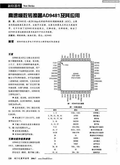
8-Bit, 250 MSPS3.3 V A/D ConverterAD9481 Rev.0Information furnished by Analog Devices is believed to be accurate and reliable.However, no responsibility is assumed by Analog Devices for its use, nor for anyinfringements of patents or other rights of third parties that may result from its use. Specifications subject to change without notice. No license is granted by implication or otherwise under any patent or patent rights of Analog Devices. Trademarks and registered trademarks are the property of their respective owners.One Technology Way, P.O. Box 9106, Norwood, MA 02062-9106, U.S.A. Tel: Fax: 781.326.8703© 2004 Analog Devices, Inc. All rights reserved.FEATURESDNL = ±0.35 LSBINL = ±0.26 LSBSingle 3.3 V supply operation (3.0 V to 3.6 V) Power dissipation of 439 mW at 250 MSPS 1 V p-p analog input rangeInternal 1.0 V referenceSingle-ended or differential analog inputs De-multiplexed CMOS outputsPower-down modeClock duty cycle stabilizerAPPLICATIONSDigital oscilloscopesInstrumentation and measurement CommunicationsPoint-to-point radiosDigital predistortion loops FUNCTIONAL BLOCK DIAGRAM545-1Figure 1.GENERAL DESCRIPTIONThe AD9481 is an 8-bit, monolithic analog-to-digital converter (ADC) optimized for high speed and low power consumption. Small in size and easy to use, the product operates at a250 MSPS conversion rate, with excellent linearity and dynamic performance over its full operating range.To minimize system cost and power dissipation, the AD9481 includes an internal reference and track-and-hold circuit. The user only provides a 3.3 V power supply and a differential encode clock. No external reference or driver components are required for many applications.The digital outputs are TTL/CMOS-compatible with an option of twos complement or binary output format. The output data bits are provided in an interleaved fashion along with output clocks that simplifies data capture. The AD9481 is available in a Pb-free, 44-lead, surface-mount package (TQFP-44) specified over the industrial temperature range (−40°C to +85°C).PRODUCT HIGHLIGHTS1.Superior linearity. A DNL of ±0.35 makes the AD9481 suitable for many instrumentation and measurement applications2.Power-down mode. A power-down function may be exercised to bring total consumption down to 15 mW.3.De-multiplexed CMOS outputs allow for easy interfacing with low cost FPGAs and standard logic.AD9481Rev. 0 | Page 2 of 28TABLE OF CONTENTSDC Specifications.............................................................................3 Digital Specifications........................................................................4 AC Specifications..............................................................................5 Switching Specifications..................................................................6 Timing Diagram...........................................................................7 Absolute Maximum Ratings............................................................8 Explanation of Test Levels...........................................................8 ESD Caution..................................................................................8 Pin Configuration and Function Descriptions.............................9 Terminology....................................................................................10 Typical Performance Characteristics...........................................12 Equivalent Circuits.........................................................................16 Applications.....................................................................................17 Analog Inputs..............................................................................17 Voltage Reference.......................................................................17 Clocking the AD9481.................................................................19 DS Inputs.....................................................................................19 Digital Outputs...........................................................................20 Interleaving Two AD9481s........................................................20 Data Clock Out...........................................................................20 Power-Down Input.....................................................................20 AD9481 Evaluation Board............................................................21 Power Connector........................................................................21 Analog Inputs..............................................................................21 Gain..............................................................................................21 Optional Operational Amplifier...............................................21 Clock............................................................................................21 Optional Clock Buffer...............................................................21 DS.................................................................................................21 Optional XTAL...........................................................................22 Voltage Reference.......................................................................22 Data Outputs...............................................................................22 Evaluation Board Bill of Materials (BOM).................................23 PCB Schematics..............................................................................24 PCB Layers......................................................................................26 Outline Dimensions.......................................................................28 Ordering Guide.. (28)REVISION HISTORY10/04—Revision 0: Initial VersionAD9481Rev. 0 | Page 3 of 28DC SPECIFICATIONSAVDD = 3.3 V , DRVDD = 3.3 V; T MIN = −40°C, T MAX = +85°C, A IN = −1 dBFS, full scale = 1.0 V , internal reference, differential analog and clock inputs, unless otherwise noted. Table 1.AD9481-250 Parameter Temp Test Level M in Typ M ax Unit RESOLUT ON 8 Bits ACCURACY No Missing Codes Full VI Guaranteed Offset Error 25°C I −40 40 mV Gain Error 125°C I −6.0 6.0 % FS Differential Nonlinearity (DNL) Full VI −0.85 ±0.35 0.85 LSB Integral Nonlinearity (INL) Full VI −0.9 ±0.26 0.9 LSB TEMPERATURE DRIFT Offset Error Full V 30 µV/°C Gain Error Full V 0.03 % FS/°C Reference Full V ±0.025 mV/°C REFERENCE Internal Reference Voltage Full VI 0.97 1.0 1.03 VOutput Current 225°C I V 1.5 mA I VREF Input Current 325°C I 100 µAI SENSE Input Current 225°C I 10 µA ANALOG INPUTS (VIN+, VIN−) Differential Input Voltage Range 4Full V 1 V p-p Common-Mode Voltage Full VI 1.6 1.9 2.1 V Input Resistance Full VI 8.4 10 11.2 kΩ Input Capacitance 25°C V 4 pF Analog Bandwidth, Full Power 25°C V 750 MHz POWER SUPPLY AVDD Full I V 3.0 3.3 3.6 V DRVDD Full I V 3.0 3.3 3.6 V Supply CurrentsIAVDD 5Full V I 133 145 mAIDRVDD 5Full V I 39 42.5 mA Power Dissipation 5 25°C V 439 mW Power-Down Dissipation 25°C V 15 37 mW Power Supply Rejection Ratio (PSRR) 25°C V −4.2 mV/V1 Gain error and gain temperature coefficients are based on the ADC only (with a fixed 1 V external reference and 1 V p-p input range). 2Internal reference mode; SENSE = AGND. 3External reference mode; VREF driven by external 1.0 V reference; SENSE = AVDD. 4In FS = 1 V, both analog inputs are 500 mV p-p and out of phase with each other. 5Supply current measured with rated encode and a 20 MHz analog input. Power dissipation measured with dc input, see the T section for power vs. clock rate.erminologyAD9481Rev. 0 | Page 4 of 28DIGITAL SPECIFICATIONSAVDD = 3.3 V , DRVDD = 3.3 V; T MIN = −40°C, T MAX = +85°C, A IN = −1 dBFS, full scale = 1.0 V , internal reference, differential analog and clock inputs, unless otherwise noted. Table 2.AD9481-250 Parameter Temp Test Level M in Typ M ax Unit CLOCK AND DS INPUTS (CLK+, CLK−, DS+, DS−) Differential Input Full IV 200 mV p-pCommon-Mode Voltage 1Full V I 1.38 1.5 1.68 V Input Resistance Full VI 4.2 5.5 6.0 kΩ Input Capacitance 25°C V 4 pF LOGIC INPUTS (PDWN, S1) Logic 1 Voltage Full IV 2.0 V Logic 0 Voltage Full IV 0.8 V Logic 1 Input Current Full VI ±160 µA Logic 0 input Current Full VI 10 µA Input Resistance 25°C V 30 kΩ Input Capacitance 25°C V 4 pF DIGITAL OUTPUTS Logic 1 Voltage 2Full VI DRVDD − 0.05 mV Logic 0 Voltage Full VI 0.05 V Output Coding Full IV Twos complement or binary1 The common mode for CLOCK inputs can be externally set, such that 0.9 V < CLK ± < 2.6 V. 2Capacitive loading only.AD9481Rev. 0 | Page 5 of 28AC SPECIFICATIONSAVDD = 3.3 V , DRVDD = 3.3 V; T MIN = −40°C, T MAX = +85°C, A IN = −1 dBFS, full scale = 1.0 V , internal reference, differential analog and clock inputs, unless otherwise noted. Table 3.AD9481-250 Parameter Temp Test Level M in Typ M ax Unit SIGNAL-TO-NOISE RATIO (SNR) f IN = 19.7 MHz 25°C V 46 dB f IN = 70.1 MHz 25°C I 44.5 45.7 dB SIGNAL-TO-NOISE AND DISTORTION (SINAD) f IN = 19.7 MHz 25°C V 45.9 dB f IN = 70.1 MHz 25°C I 44.4 45.7 dB EFFECTIVE NUMBER OF BITS (ENOB) f IN = 19.7 MHz 25°C V 7.5 Bits f IN = 70.1 MHz 25°C I 7.2 7.5 Bits WORST SECOND OR THIRD HARMONIC DISTORTION f IN = 19.7 MHz 25°C V −64.8 dBc f IN = 70.1 MHz 25°C I −64.8 −54 dBcWORST OTHERf IN = 19.7 MHz 25°C V −68 dBc f IN = 70.1 MHz 25°C I −65.8 −56 dBcSPURIOUS-FREE DYNAMIC RANGE (SFDR)1f IN = 19.7 MHz 25°C V −64.8 dBc f IN = 70.1 MHz 25°C I −64.8 −54 dBcTWO-TONE INTERMODULATION DISTORTION (IMD)f IN1 = 69.3 MHz, f IN2 = 70.3 MHz 25°C V −64.9 dBc1DC and Nyquist bin energy ignored.AD9481Rev. 0 | Page 6 of 28SWITCHING SPECIFICATIONSAVDD = 3.3 V , DRVDD = 3.3 V; differential encode input, duty cycle stabilizer enabled, unless otherwise noted. Table 4.AD9481-250 Parameter Temp Test Level M in Typ M ax Unit CLOCK Maximum Conversion Rate Full VI 250 MSPS Minimum Conversion Rate Full IV 20 MSPS Clock Pulse-Width High (t EH ) Full I V 1.2 2 ns Clock Pulse-Width Low (t EL ) Full I V 1.2 2 ns DS Input Setup Time (t SDS ) Full I V 0.5 ns DS Input Hold Time (t HDS ) Full I V 0.5 ns OUTPUT PARAMETERS 1Valid Time (t V )2Full V I 2.5 ns Propagation Delay (t PD ) Full VI 4 5.4 ns Rise Time (t R ) 10% to 90% Full V 670 ps Fall Time (t F ) 10% to 90% Full V 360 ps DCO Propagation Delay (t CPD ) 3Full V I 2.5 3.9 5.3 nsData-to-DCO Skew (t PD − t CPD )4Full V I −0.5 +0.5 ns A Port Data to DCO− Rising (t SKA )5Full I V 4 ns B Port Data to DCO+ Rising (t SKB ) Full IV 4 ns Pipeline Latency (A, B) Full IV 8 Cycles APERTURE Aperture Delay (t A ) 25°C V 1.5 ns Aperture Uncertainty (Jitter) 25°C V 0.25 ps rms OUT-OF-RANGE RECOVERY TIME 25°C V 1 Cycle1 C LOAD equals 5 pF maximum for all output switching specifications. 2Valid time is approximately equal to minimum t PD . 3T CPD equals clock rising edge to DCO (+ or −) rising edge delay. 4Data changing to (DCO+ or DCO−) rising edge delay. 5T SKA , T SKB are both clock rate dependent delays equal to T CYCLE − (Data to DCO skew).AD9481Rev. 0 | Page 7 of 28TIMING DIAGRAMVINCLK+CLK–D7A TO D0APORT A DS+DS–DCO+DCO–Figure 2. Timing DiagramAD9481Rev. 0 | Page 8 of 28ABSOLUTE MAXIMUM RATINGSThermal impedance (θJA ) = 46.4°C/W (4-layer PCB). Table 5.Parameter Min. Rating Max. Rating ELECTR CAL AVDD (With respect to AGND) −0.5 V +4.0 V DRVDD (With respect to DRGND) −0.5 V +4.0 V AGND (With respect to DRGND) −0.5 V +0.5 V Digital I/0 (With respect to DRGND) −0.5 V DRVDD + 0.5 V Analog Inputs (With respect to AGND) −0.5 V AVDD + 0.5 V ENV RONMENTAL Operating Temperature −40°C +85°CJunction Temperature 150°CStorage Temperature 150°CStresses above those listed under Absolute Maximum Ratings may cause permanent damage to the device. This is a stress rating only; functional operation of the device at these or any other conditions above those indicated in the operationalsection of this specification is not implied. Exposure to absolute maximum rating conditions for extended periods may affect device reliability. EXPLANATION OF TEST LEVELSTable 6.Level Description I100% production tested.II 100% production tested at 25°C and guaranteed by design and characterization at specified temperatures.III Sample tested only.IV Parameter is guaranteed by design and characterization testing.V Parameter is a typical value only.VI 100% production tested at 25°C and guaranteed bydesign and characterization for industrial temperaturerange.ESD CAUTIONESD (electrostatic discharge) sensitive device. Electrostatic charges as high as 4000 V readily accumulateon the human body and test equipment and can discharge without detection. Although this product features proprietary ESD protection circuitry, permanent damage may occur on devices subjected to high energy electrostatic discharges. Therefore, proper ESD precautions are recommended to avoid performance degradation or loss of functionality.AD9481Rev. 0 | Page 9 of 28PIN CONFIGURATION AND FUNCTION DESCRIPTIONSCLK–AVDD AGNDD7A (MSB)DRGND DRVDD CLK+D6A D5AD4A D3A AGND AVDD AVDD DRGND S1PDWN SENSE D7B (MSB)D6B D5B D4BD 2AD 1AD 0A (L S B )D R G N DD C O –D C O +D R V D DD 0B (L S B )D 1BD 2BD 3BD S +D S –S 3A V D DA G N DV I N +V I N –A G N DA V D DA G N DV R E F05045-003Figure 3. Pin ConfigurationTable 7. Pin Function DescriptionsPinNo. Name Description 1 CLK+ Input Clock—True 2 CLK− Input Clock—Complement 3 AVDD 3.3 V Analog Supply 4 AGND Analog Ground 5 DRVDD 3.3 V Digital Output Supply 6 DRGND Digital Ground 7 D7A Data Output Bit 7—Channel A (MSB) 8 D6A Data Output Bit 6—Channel A 9 D5A Data Output Bit 5—Channel A 10 D4A Data Output Bit 4—Channel A 11 D3A Data Output Bit 3—Channel A 12 D2A Data Output Bit 2—Channel A 13 D1A Data Output Bit 1—Channel A 14 D0A Data Output Bit 0—Channel A (LSB) 15 DRGND Digital Ground 16 DCO− Data Clock Output—Complement 17 DCO+ Data Clock Output—True 18 DRVDD 3.3 V Digital Output Supply 19 D0B Data Output Bit 0—Channel B (LSB) 20 D1B Data Output Bit 1—Channel B 21 D2B Data Output Bit 2—Channel B 22 D3B Data Output Bit 3—Channel B 23 D4B Data Output Bit 4—Channel B 24 D5B Data Output Bit 5—Channel BPinNo. Name Description 25 D6B Data Output Bit 6—Channel B 26 D7B Data Output Bit 7—Channel B (MSB) 27 DRGND Digital Ground28 S1 Data Format Select and Duty Cycle StabilizerSelect29 PDWN Power-Down Selection 30 AVDD 3.3 V Analog Supply 31 AVDD 3.3 V Analog Supply 32 AGND Analog Ground 33 SENSE Reference Mode Selection 34 VREF Voltage Reference Input/Output 35 AGND Analog Ground 36 AVDD 3.3 V Analog Supply 37 AGND Analog Ground 38 V I N− Analog I nput—Complement 39 V I N+ Analog I nput—True 40 AGND Analog Ground 41 AVDD 3.3 V Analog Supply42 S3 DCO Enable Select (Tie to AVDD for DCOActive)43 DS− Data Sync Complement (If Unused, Tie toDRVDD)44 DS+ Data Sync True (If Unused, Tie to DGND)AD9481Rev. 0 | Page 10 of 28TERMINOLOGYAnalog BandwidthThe analog input frequency at which the spectral power of the fundamental frequency (as determined by the FFT analysis) is reduced by 3 dB.Aperture DelayThe delay between the 50% point of the rising edge of the encode command and the instant the analog input is sampled. Aperture Uncertainty (Jitter)The sample-to-sample variation in aperture delay.Clock Pulse-Width/Duty CyclePulse-width high is the minimum amount of time that the clock pulse should be left in a Logic 1 state to achieve ratedperformance; pulse-width low is the minimum time clock pulse should be left in a low state. See timing implications of changing t EH in the Clocking the AD9481 section. At a given clock rate, these specifications define an acceptable clock duty cycle. CrosstalkCoupling onto one channel being driven by a low level (−40 dBFS) signal when the adjacent interfering channel is driven by a full-scale signal.Differential Analog Input Resistance, Differential Analog Input Capacitance, and Differential Analog Input Impedance The real and complex impedances measured at each analog input port. The resistance is measured statically and the capacitance and differential input impedances are measured with a network analyzer.Differential Analog Input Voltage RangeThe peak-to-peak differential voltage that must be applied to the converter to generate a full-scale response. Peak differential voltage is computed by observing the voltage on a single pin and subtracting the voltage from the other pin, which is 180° out of phase. Peak-to-peak differential is computed by rotating the inputs phase 180° and taking the peak measurement again. The difference is then computed between both peak measurements.Differential NonlinearityThe deviation of any code width from an ideal 1 LSB step. Effective Number of Bits (ENOB)ENOB is calculated from the measured SINAD based on the equation (assuming full-scale input)6.02dB1.76−=MEASURED SINAD ENOBFull-Scale Input PowerExpressed in dBm. Computed using the following equation⎟⎟⎟⎟⎟⎠⎞⎜⎜⎜⎜⎜⎝⎛=0.001log 10INPUT FULLSCALE 2FULLSCALE Z rms V Power Gain ErrorGain error is the difference between the measured and ideal full-scale input voltage range of the ADC.Harmonic Distortion, SecondThe ratio of the rms signal amplitude to the rms value of the second harmonic component, reported in dBc.Harmonic Distortion, ThirdThe ratio of the rms signal amplitude to the rms value of the third harmonic component, reported in dBc.Integral NonlinearityThe deviation of the transfer function from a reference line measured in fractions of 1 LSB using a best straight line determined by a least square curve fit.Minimum Conversion RateThe encode rate at which the SNR of the lowest analog signal frequency drops by no more than 3 dB below the guaranteed limit.Maximum Conversion RateThe encode rate at which parametric testing is performed. Output Propagation DelayThe delay between a differential crossing of CLK+ and CLK− and the time when all output data bits are within valid logic levels.Noise (for Any Range within the ADC)This value includes both thermal and quantization noise.⎟⎟⎠⎞⎜⎜⎝⎛−−××=1010.0010Z dBFSdBc dBm noise Signal SNR FS V where:Z is the input impedance.FS is the full scale of the device for the frequency in question. SNR is the value for the particular input level.Signal is the signal level within the ADC reported in dB below full scale.分销商库存信息:ANALOG-DEVICESAD9481BSUZ-250AD9481-PCBZ。