AT45DB161B中文资料
- 格式:pdf
- 大小:351.52 KB
- 文档页数:33
Description
The AT45DB161B is a 2.5-volt or 2.7-volt only, serial interface Flash memory ideally suited for a wide variety of digital voice-, image-, program code- and data-storage
Features
• Single 2.5V - 3.6V or 2.7V - 3.6V Supply • Serial Peripheral Interface (SPI) Compatible • 20 MHz Max Clock Frequency • Page Program Operation
– Single Cycle Reprogram (Erase and Program)
– 4096 Pages (528 Bytes/Page) Main Memory • Supports Page and Block Erase Operations • Two 528-byte SRAM Data Buffers – Allows Receiving of Data
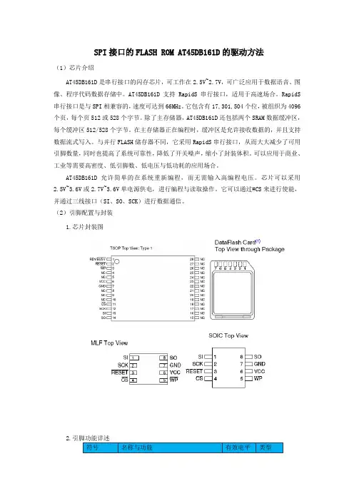
Pin Configurations
Pin Name CS SCK SI SO WP
RESET RDY/BUSY
Function Chip Select Serial Clock Serial Input Serial Output Hardware Page Write Protect Pin Chip Reset Ready/Busy
SECTOR 2
BLOCK 62 BLOCK 63 BLOCK 64 BLOCK 65 BLOCK 66
8 Pages
BLOCK 1
BLOCK 0
PAGE ARCHITECTURE
PAGE 0 PAGE 1
PAGE 6 PAGE 7 PAGE 8 PAGE 9
PAGE 14 PAGE 15 PAGE 16 PAGE 17 PAGE 18
WP
24
RESET
23
RDY/BUSY
22
NC
21
NC
20
NC
19
ห้องสมุดไป่ตู้NC
18
NC
17
NC
16
NC
15
NC
CBGA Top View through Package
12345
A NC NC NC NC
B NC SCK GND VCC NC
C NC CS RDY/BSY WP NC
D NC SO SI RESET NC
CS 4
8 SO 7 GND 6 VCC 5 WP
Rev. 2224I–DFLSH–10/04
1
Block Diagram
applications. Its 17,301,504 bits of memory are organized as 4096 pages of 528 bytes each. In addition to the main memory, the AT45DB161B also contains two SRAM data buffers of 528 bytes each. The buffers allow receiving of data while a page in the main memory is being reprogrammed, as well as writing a continuous data stream. EEPROM emulation (bit or byte alterability) is easily handled with a self-contained three step Read-Modify-Write operation.Unlike conventional Flash memories that are accessed randomly with multiple address lines and a parallel interface, the DataFlash uses a SPI serial interface to sequentially access its data. DataFlash supports SPI mode 0 and mode 3. The simple serial interface facilitates hardware layout, increases system reliability, minimizes switching noise, and reduces package size and active pin count. The device is optimized for use in many commercial and industrial applications where high density, low pin count, low voltage, and low power are essential. The device operates at clock frequencies up to 20 MHz with a typical active read current consumption of 4 mA.
SECTOR 0
BLOCK ARCHITECTURE
BLOCK 0 BLOCK 1
SECTOR 1
SECTOR 2 = 256 Pages 135,168 bytes (128K + 4K)
SECTOR 3 = 256 Pages 135,168 bytes (128K + 4K)
BLOCK 30 BLOCK 31 BLOCK 32 BLOCK 33
SECTOR 16 = 256 Pages 135,168 bytes (128K + 4K)
Device Operation
Read Commands
2224I–DFLSH–10/04
BLOCK 509 BLOCK 510 BLOCK 511
Block = 4224 bytes (4K + 128)
– 4 mA Active Read Current Typical
– 2 µA CMOS Standby Current Typical • Hardware Data Protection Feature • 100% Compatible to AT45DB161 • 5.0V-tolerant Inputs: SI, SCK, CS, RESET and WP Pins • Commercial and Industrial Temperature Ranges • Green (Pb/Halide-free) Packaging Options
28 NC 27 NC 26 NC 25 NC 24 NC 23 NC 22 NC 21 NC 20 NC 19 NC 18 NC 17 NC 16 NC 15 NC
SOIC
GND
1
NC
2
NC
3
CS
4
SCK
5
SI
6
SO
7
NC
8
NC
9
NC
10
NC
11
NC
12
NC
13
NC
14
28
VCC
27
NC
26
NC
25
PAGE 4093 PAGE 4094 PAGE 4095
Page = 528 bytes (512 + 16)
The device operation is controlled by instructions from the host processor. The list of instructions and their associated opcodes are contained in Tables 1 through 4. A valid instruction starts with the falling edge of CS followed by the appropriate 8-bit opcode and the desired buffer or main memory address location. While the CS pin is low, toggling the SCK pin controls the loading of the opcode and the desired buffer or main memory address location through the SI (serial input) pin. All instructions, addresses and data are transferred with the most significant bit (MSB) first.
E NC NC NC NC NC
16-megabit 2.5-volt Only or 2.7-volt Only DataFlash®
AT45DB161B
Note: 1. See AT45DCB002 Datasheet.
CASON – Top View through Package
SI 1 SCK 2 RESET 3
while Reprogramming of Nonvolatile Memory • Continuous Read Capability through Entire Array
– Ideal for Code Shadowing Applications • Low Power Dissipation