三极管开关特性(经典)
- 格式:ppt
- 大小:387.50 KB
- 文档页数:14

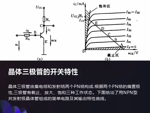
三极管的开关特性
在脉冲与数字电路中,三极管作为最基本的开关元件得到了普遍的应用。
三极管工作在饱和状态时,其UCES≈0,相当于开关的接通状态;工
作在截止状态时,IC≈0,相当于开关的断开状态,因此,三极管可当
做开关器件使用。
结型场效应管
场效应管(Fjeld Effect Transistor简称FET )是利用电场效应来控制半导体中电流的一种半导体器件,故因此而得名。
场效应管是一种电压控制器件,只依靠一种载流子参与导电,故又称为单极型晶体管。
与双极型晶体三极管
相比,它具有输入阻抗高、噪声低、热稳定性好、抗辐射能力强、功耗小、
制造工艺简单和便于集成化等优点。
场效应管有两大类,结型场效应管JFET和绝缘栅型场效应管IGFET,后
者性能更为优越,发展迅速,应用广泛。
图Z0121 为场效应管的类型及图形、符号。
一、结构与分类
图Z0122为N沟道结型场效应管结构示意图和它的图形、符号。
它是在同。
三极管的开关特性在脉冲与数字电路中,三极管作为最基本的开关元件得到了普遍的应用。
三极管工作在饱和状态时,其UCES≈0,相当于开关的接通状态;工作在截止状态时,IC≈0,相当于开关的断开状态,因此,三极管可当做开关器件使用。
结型场效应管场效应管(Fjeld Effect Transistor简称FET )是利用电场效应来控制半导体中电流的一种半导体器件,故因此而得名。
场效应管是一种电压控制器件,只依靠一种载流子参与导电,故又称为单极型晶体管。
与双极型晶体三极管相比,它具有输入阻抗高、噪声低、热稳定性好、抗辐射能力强、功耗小、制造工艺简单和便于集成化等优点。
场效应管有两大类,结型场效应管JFET和绝缘栅型场效应管IGFET,后者性能更为优越,发展迅速,应用广泛。
图Z0121 为场效应管的类型及图形、符号。
一、结构与分类图 Z0122为N沟道结型场效应管结构示意图和它的图形、符号。
它是在同一块N型硅片的两侧分别制作掺杂浓度较高的P型区(用P+表示),形成两个对称的PN结,将两个P区的引出线连在一起作为一个电极,称为栅极(g),在N型硅片两端各引出一个电极,分别称为源极(s)和漏极(d)。
在形成PN结过程中,由于P+区是重掺杂区,所以N一区侧的空间电荷层宽度远大二、工作原理N沟道和P沟道结型场效应管的工作原理完全相同,只是偏置电压的极性和载流子的类型不同而已。
下面以N沟道结型场效应管为例来分析其工作原理。
电路如图Z0123所示。
由于栅源间加反向电压,所以两侧PN结均处于反向偏置,栅源电流几乎为零。
漏源之间加正向电压使N型半导体中的多数载流子-电子由源极出发,经过沟道到达漏极形成漏极电流ID。
1.栅源电压UGS对导电沟道的影响(设UDS=0)在图Z0123所示电路中,UGS <0,两个PN结处于反向偏置,耗尽层有一定宽度,ID=0。
若|UGS| 增大,耗尽层变宽,沟道被压缩,截面积减小,沟道电阻增大;若|UGS| 减小,耗尽层变窄,沟道变宽,电阻减小。

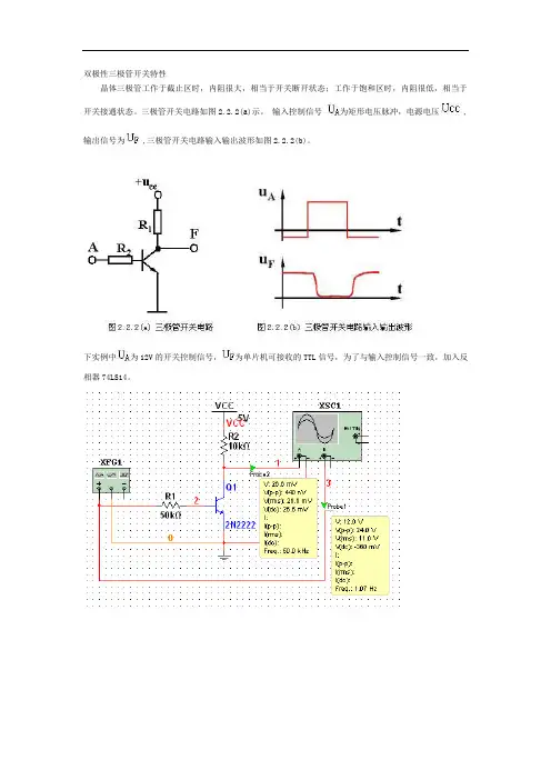
双极性三极管开关特性晶体三极管工作于截止区时,内阻很大,相当于开关断开状态;工作于饱和区时,内阻很低,相当于开关接通状态。
三极管开关电路如图2.2.2(a)示。
输入控制信号为矩形电压脉冲,电源电压 ,输出信号为 ,三极管开关电路输入输出波形如图2.2.2(b)。
下实例中为12V的开关控制信号,为单片机可接收的TTL信号,为了与输入控制信号一致,加入反相器74LS14。
TransistorsA Transistor is a solid-state device designed to control DC current. Transistors are most commonly found in low DC powered sensors as the output switch. There are two types of transistors - NPN and PNP.The figure below shows a NPN (Current Sink) Open Collector TransistorFigure 1: Sensor NPN OutputOutput StyleDepending on model, incremental encoders are available with several different electrical output styles. Choice of signal depends on receiving instrument and cable distance. Line driver outputs with complimentary outputs can be used with longer cables as noise spikes can be cancelled.NPNUses an NPN type transistor and aninternal resistor pulling up to the powersupply rail. The output is an activevoltage.NPN Open CollectorUses an NPN type transistor butwithout an internal pull up resistor tothe supply rail. The output is passiveso a separate power supply can beused.PNPUses a PNP type transistor and aninternal resistor pulling down to zerovolts.PNP Open CollectorUses a PNP type transistor but withoutan internal pull down resistor to zerovolts.Push PullA problem with NPN and PNP typeoutputs is the high output impedance.This can be solved by acomplementary output allowing betterswitching to zero and positive supplyrails.Line DriverThis output style has twocomplimentary outputs per channelallowing better transmission in noisyenvironments and long cable lengths.The receiver can process the signal,eliminating noise spikes.PTC protectionA positive temperature coefficientresistor can be added to the output of aNPN or PNP encoder, protecting itfrom output short circuits.Sinking/SourcingSinking sensors allow current to flow into the sensor to the voltage common, while sourcing sensors allow current to flow out of the sensor from a positive source. For both of these methods the emphasis is on current flow, not voltage. By usingcurrent flow, instead of voltage, many of the electrical noise problems are reduced. When discussing sourcing and sinking we are referring to the output of the sensor that is acting like a switch. In fact the output of the sensor is normally a transistor, that will act like a switch (with some voltage loss). A PNP transistor is used for the sourcing output, and an NPN transistor is used for the sinking input. Whendiscussing these sensors the term sourcing is often interchanged with PNP, and sinking with NPN. A simplified example of a sinking output sensor is shown in See A Simplified NPN/Sinking Sensor. The sensor will have some part that dealswith detection, this is on the left. The sensor needs a voltage supply to operate, so a voltage supply is needed for the sensor. If the sensor has detected somephenomenon then it will trigger the active line. The active line is directlyconnected to an NPN transistor. (Note: for an NPN transistor the arrow always points away from the center.) If the voltage to the transistor on the active line is 0V, then the transistor will not allow current to flow into the sensor. If the voltage on the active line becomes larger (say 12V) then the transistor will switch on andallow current to flow into the sensor to the common.A Simplified NPN/Sinking SensorSourcing sensors are the complement to sinking sensors. The sourcing sensors use a PNP transistor, as shown in See A Simplified Sourcing/PNP Sensor. (Note: PNP transistors are always drawn with the arrow pointing to the center.) When thesensor is inactive the active line stays at the V+ value, and the transistor staysswitched off. When the sensor becomes active the active line will be made 0V, and the transistor will allow current to flow out of the sensor.A Simplified Sourcing/PNP SensorMost NPN/PNP sensors are capable of handling currents up to a few amps, and they can be used to switch loads directly. (Note: always check the documentation for rated voltages and currents.) An example using sourcing and sinking sensors to control lights is shown in See Direct Control Using NPN/PNP Sensors. (Note: This example could be for a motion detector that turns on lights in dark hallways.)Direct Control Using NPN/PNP SensorsIn the sinking system in See Direct Control Using NPN/PNP Sensors the light has V+ applied to one side. The other side is connected to the NPN output of the sensor.When the sensor turns on the current will be able to flow through the light, into the output to V- common. (Note: Yes, the current will be allowed to flow into the output for an NPN sensor.) In the sourcing arrangement the light will turn on when the output becomes active, allowing current to flow from the V+, thought thesensor, the light and to V- (the common).At this point it is worth stating the obvious - The output of a sensor will be an input for a PLC. And, as we saw with the NPN sensor, this does not necessarily indicate where current is flowing. There are two viable approaches for connecting sensors to PLCs. The first is to always use PNP sensors and normal voltage input cards.The second option is to purchase input cards specifically designed for sourcing or sinking sensors. An example of a PLC card for sinking sensors is shown in See A PLC Input Card for Sinking Sensors.A PLC Input Card for Sinking Sensors“采用集电极开路的输出方式,有什么好处?”A:集电极开路输出大概有以下几个好处:1.可以实现线与功能,即两个或多个输出端可并联在一起,然后接一上拉电阻至高电平。
三极管典型开关电路三极管是一种非线性电子器件,常用于电子电路中的放大和开关控制。
典型的三极管开关电路有共射、共基和共集三种。
共射开关电路是最常见的一种三极管开关电路。
它的基极通过一个电阻与信号源相连,发射极通过负载电阻连接至地,而集电极则连接到一个正电源。
在开关状态下,当输入信号高于一个阈值电压时,三极管将会被打开,并且电流可以从集电极流向发射极。
而当输入信号低于阈值电压时,三极管关断,电流无法通过。
由于集电极端的电阻,该电路可以输出一个较高的电压。
共基开关电路中,集电极连接到一个电压源上,发射极通过一个负载电阻与地相连,而基极则与信号源相连。
在开关状态下,当输入信号高于一个阈值电压时,三极管被打开,电流从集电极流向发射极,而当输入信号低于阈值电压时,三极管关断,电流无法通过。
共基开关电路可以提供较低的输出电压,常用于需要较高的电流放大的场景。
共集开关电路中,发射极连接到一个电压源上,基极通过一个电阻与信号源相连,而集电极则通过一个负载电阻与地相连。
在开关状态下,当输入信号高于一个阈值电压时,三极管被关闭,电流无法从集电极流向发射极,而当输入信号低于阈值电压时,三极管打开,电流可以通过。
共集开关电路可以提供较低的输出电压,而且具有电流放大的特性。
三极管开关电路的工作原理是,通过输入信号的控制,将三极管的工作状态切换为导通或者截止。
通过这种方式,我们可以将电路中的信号进行放大、开关控制等操作。
总结来说,三极管典型的开关电路主要有共射、共基和共集三种。
它们通过控制输入信号的大小,使三极管处于导通或截止状态,从而实现电路的特定功能。
这些典型的开关电路在电子电路设计中广泛应用,并且有着不同的电压输出特性和电流放大特性。

三极管典型开关电路三极管是一种常用的半导体器件,在电路中起着非常重要的作用。
其中,三极管的典型开关电路是一种常见且广泛应用的电路,用于实现对电路的开关控制。
下面将对三极管典型开关电路进行详细介绍。
三极管典型开关电路通常由三极管、电阻、电源等元器件组成。
其基本原理是通过控制三极管的输入信号,使得三极管处于导通或截止状态,从而实现电路的开关控制。
在三极管典型开关电路中,通常会采用双极型晶体管(NPN型或PNP型)来实现开关功能。
在NPN型三极管典型开关电路中,当输入信号为低电平时,三极管处于截止状态,电路中的电流无法流通,此时电路处于断开状态;当输入信号为高电平时,三极管处于饱和状态,电路中的电流可以流通,此时电路处于闭合状态。
通过控制输入信号的高低电平,可以实现对电路的开关控制。
在PNP型三极管典型开关电路中,其工作原理与NPN型相反。
当输入信号为高电平时,三极管处于截止状态,电路处于断开状态;当输入信号为低电平时,三极管处于饱和状态,电路处于闭合状态。
同样,通过控制输入信号的高低电平,可以实现对电路的开关控制。
三极管典型开关电路在实际电路设计中具有广泛的应用。
例如,可以用于数字电路中的开关控制、电源管理电路中的电路保护等方面。
此外,三极管的开关电路还可以实现电路的时序控制、电路的选择性切换等功能,极大地提高了电路的灵活性和可控性。
总的来说,三极管典型开关电路是一种常见且实用的电路,通过控制三极管的开关状态,可以实现对电路的开关控制。
在电子电路设计和应用中,三极管开关电路发挥着重要的作用,为电路的实现和功能的实现提供了关键的支持。
希望通过本文的介绍,读者对三极管典型开关电路有了更深入的了解,可以更好地应用于实际电路设计中。
第一节二极管的开关特性一般而言,开关器件具有两种工作状态:第一种状态被称为接通,此时器件的阻抗很小,相当于短路;第二种状态是断开,此时器件的阻抗很大,相当于开路。
在数字系统中,晶体管基本上工作于开关状态。
对开关特性的研究,就是具体分析晶体管在导通和截止之间的转换问题。
晶体管的开关速度可以很快,可达每秒百万次数量级,即开关转换在微秒甚至纳秒级的时间内完成。
二极管的开关特性表现在正向导通与反向截止这样两种不同状态之间的转换过程。
二极管从反向截止到正向导通与从正向导通到反向截止相比所需的时间很短,一般可以忽略不计,因此下面着重讨论二极管从正向导通到反向截止的转换过程。
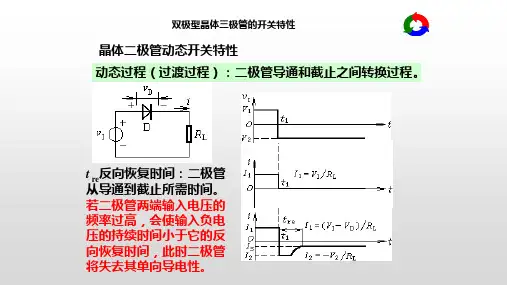
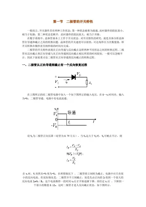
一、二极管从正向导通到截止有一个反向恢复过程在上图所示的硅二极管电路中加入一个如下图所示的输入电压。
在0―t1时间内,输入为+V F,二极管导通,电路中有电流流通。
设V D为二极管正向压降(硅管为0.7V左右),当V F远大于V D时,V D可略去不计,则在t1时,V1突然从+V F变为-V R。
在理想情况下,二极管将立刻转为截止,电路中应只有很小的反向电流。
但实际情况是,二极管并不立刻截止,而是先由正向的I F变到一个很大的反向电流I R=V R/R L,这个电流维持一段时间t S后才开始逐渐下降,再经过t t后,下降到一个很小的数值0.1I R,这时二极管才进人反向截止状态,如下图所示。
通常把二极管从正向导通转为反向截止所经过的转换过程称为反向恢复过程。
其中t S 称为存储时间,t t称为渡越时间,t re=t s+t t称为反向恢复时间。
由于反向恢复时间的存在,使二极管的开关速度受到限制。
二、产生反向恢复过程的原因——电荷存储效应产生上述现象的原因是由于二极管外加正向电压V F时,载流子不断扩散而存储的结果。
当外加正向电压时P区空穴向N区扩散,N区电子向P区扩散,这样,不仅使势垒区(耗尽区)变窄,而且使载流子有相当数量的存储,在P区内存储了电子,而在N区内存储了空穴,它们都是非平衡少数载流于,如下图所示。

三极管典型开关电路三极管是一种常用的电子元件,可以用来实现各种电路功能。
其中,三极管的典型开关电路广泛应用于数码电子产品、功率控制电路等领域。
下面将从三极管的基本工作原理、典型的开关电路及其应用展开阐述。
三极管是由三个控制极(基极、发射极、集电极)组成,一般用来放大电流或者作为开关使用。
在开关电路中,三极管的工作状态有两种,即饱和状态和截止状态。
在饱和状态时,三极管导通,此时基极发出的微弱电流会放大成较大的电流输出;而在截止状态时,三极管不导电,无输出电流。
通过改变基极电压或者基极电流来控制三极管的工作状态,从而实现开关电路的功能。
典型的三极管开关电路有两种,分别是共发射极开关电路和共集电极开关电路。
下面将分别介绍这两种开关电路及其应用。
首先是共发射极开关电路。
这种电路结构简单,常用于小功率开关电路。
该电路的输入信号通过基极到达发射极,通过改变基极电流来控制三极管的工作状态。
当基极电流较小时,三极管处于截止状态,无输出电流;而当基极电流较大时,三极管处于饱和状态,有输出电流。
这种开关电路常用于触发器、脉冲调制和数字逻辑电路等应用中。
其次是共集电极开关电路,又称为集电极开关电路。
该电路具有较高的电压放大倍数,常用于大功率开关电路。
该电路的输入信号通过基极到达发射极,基极电流控制发射极电流的大小,进而影响集电极电流。
当基极电流较小时,三极管处于截止状态,无输出电流;而当基极电流较大时,三极管处于饱和状态,有输出电流。
该开关电路常用于功率开关、计时器、电源开关和电动机驱动等应用中。
三极管的开关电路在实际应用中具有广泛的用途。
例如,三极管的共发射极开关电路可以用于控制数码电子产品中的LED灯的亮灭;而共集电极开关电路可以实现电源的开关控制和电动机的驱动控制等。
此外,三极管的开关电路也常用于功率控制电路中,如用于调光控制、变频驱动等。
这些应用使得三极管开关电路在现代电子产品中发挥着重要的作用。
总结起来,三极管典型开关电路有共发射极开关电路和共集电极开关电路。
名词解释三极管的开关特性三极管是一种重要的电子器件,常用于电子电路中的开关和放大功能。
它由三个控制层、基本层和输出层组成,具有灵活的开关特性。
在电子技术领域中,三极管的开关特性是指在特定电压和电流条件下,三极管可以实现开关的状态转换,即在低电压输入情况下传导电流,而在高电压输入情况下截断电流。
三极管的开关特性是由其特殊的结构和材料性质所决定的。
它包括两种常见类型:NPN型和PNP型。
NPN型三极管由两个P型半导体夹着一个N型半导体构成,而PNP型三极管则相反,由两个N型半导体夹着一个P型半导体构成。
这种结构可以实现电流的双向流动,并且通过控制基极电流可以实现开关的状态变化。
在三极管的开关特性中,主要存在两种工作状态:饱和状态和截止状态。
饱和状态是当三极管的输入电压高于一定阈值时,经过适当的基极电流驱动后,三极管的集电极与发射极之间的电压非常低,导致电流流过。
这种状态下,三极管相当于一个导通的开关,电流可以在电路中流动。
而截止状态则是当三极管的输入电压低于一定阈值时,三极管的集电极与发射极之间的电阻非常高,导致电流无法流过。
此时,三极管相当于一个断开的开关,电路中的电流被截断。
三极管的开关特性在电子电路中起到了重要的作用。
它可以实现逻辑门、计时器、振荡器等电路的构建。
通过控制三极管输入电压的变化,可以改变电路中的电流流向,实现不同的功能。
在数字电路中,三极管的开关特性被广泛应用于逻辑门的设计和实现。
通过组合不同的逻辑门,可以构建出各种复杂的电路,用于处理和操作数字信号。
除了在数字电路中的应用,三极管的开关特性在模拟电路中也有广泛的应用。
在放大器电路中,三极管可以作为信号放大的关键元件,通过控制输入电压的变化,实现对输入信号的放大和处理。
在功率放大电路中,三极管可以承受高电流和高功率的输入,实现对功率信号的放大和转换。
总结起来,三极管的开关特性在电子电路中起着重要的作用。
通过控制输入电压和电流条件,三极管可以实现开关的状态转换,从而实现电路功能的改变。