CCD47-20 AIMO
- 格式:pdf
- 大小:122.64 KB
- 文档页数:12
3. Test carried out at e2v technologies on all sensors.
4. Dynamic range is the ratio of readout noise to full well capacity measured at 253 K and 20 kHz readout speed.
Dynamic range (at 20 kHz) . . . *50 000:1
Spectral range . . . . . . . 400 – 1100
nm
Readout noise (at 20 kHz) . . . . . . 2.0 e7 rms
QE at 700 nm . . . . . . . . . . 45
rms e7/pixel rms e7/pixel
MHz % of mean
e7/pixel/s
Max
–
nF
–
nF
–
nF
–
pF
–
pF
–
pF
–
O
100039, page 2
# e2v technologNAL (e7 rms)
BLEMISH SPECIFICATION
e2v technologies (uk) limited, Waterhouse Lane, Chelmsford, Essex CM1 2QU, UK Telephone: +44 (0)1245 493493 Facsimile: +44 (0)1245 492492 e-mail: enquiries@ Internet: Holding Company: e2v technologies plc
5. CCD characterisation measurements made using charge generated by X-ray photons of known energy.
6. Measured using a dual-slope integrator technique (i.e. correlated double sampling) with a 20 ms integration period.
Traps
Pixels where charge is temporarily held.
Traps are counted if they have a capacity greater than 200 e7 at 253 K.
parallel serial Output amplifier responsivity (see note 3) Readout noise at 243 K (see notes 3 and 6): grade 0 and 1 grade 2 Maximum readout frequency (see note 7) Response non-uniformity (std. deviation) Dark signal non-uniformity (std. deviation) (see notes 3 and 8)
–
I1/SS and S1/SS
–
R1/R1 interphase
–
R1/(SS+DG+OD)
–
1R/SS
–
Output impedance (at typ. operating condition)
–
NOTES
1. Signal level at which resolution begins to degrade.
# e2v technologies (uk) limited 2006
A1A-100039 Issue 5, March 2006
411/9572
PERFORMANCE
Peak charge storage (see note 1) Peak output voltage (no binning) Dark signal at 293 K (see notes 2 and 3) Dynamic range (see note 4) Charge transfer efficiency (see note 5):
e2v technologies inc. 4 Westchester Plaza, PO Box 1482, Elmsford, NY10523-1482 USA Telephone: (914) 592-6050 Facsimile: (914) 592-5148 e-mail: enquiries@
Typical 100k 450 100 50 000
99.9999 99.9993 4.5
2.0 3.0 5.0 1
40
Typical 3.5 3.5 4.5 40 60 10
300
Max – –
200 –
– – 6.0
4.0 6.0 – 3
80
e7/pixel mV
e7/pixel/s
% % mV/e7
%
GENERAL DATA
Format
Image area . . . . . . . . . 13.3 x 13.3
mm
Active pixels (H) . . . . . . . . 1024
(V) . . . . . . . . 1024
Pixel size . . . . . . . . . . 13 x 13
7. Readout at speeds in excess of 5 MHz into a 15 pF load can be achieved but performance to the parameters given cannot be guaranteed.
8. Measured between 233 and 253 K, excluding white defects.
Min 60k
– – –
– – 3.0
– – – –
–
ELECTRICAL INTERFACE CHARACTERISTICS
Electrode capacitances (measured at mid-clock level)
Min
S1/S1 interphase
–
I1/I1 interphase
2. Measured between 233 and 253 K and VSS +9.0 V. Dark signal at any temperature T (kelvin) may be estimated from: Qd/Qd0 = 1.14 x 10⁶T3e79080/T where Qd0 is the dark signal at T = 293 K (20 8C). Below 230 K, additional dark current components with a weaker temperature dependence may become significant.
APPLICATIONS
* Spectroscopy
* Scientific Imaging
* Star Tracking
* Medical Imaging
INTRODUCTION
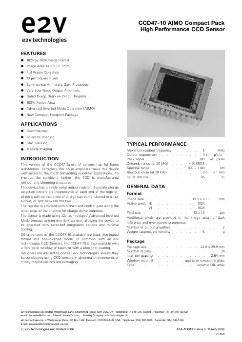
This version of the CCD47-20 is a front-face illuminated, frame transfer CCD sensor with high performance low noise output amplifiers, suitable for use in slow-scan imaging systems. The image area contains a full 1024 by 1024 pixels which are 13 mm square. The output register is split, allowing either or both of the two output amplifiers to be employed, and is provided with a drain and control gate for charge dump purposes. The sensor is made using e2v technologies’ Advanced Inverted Mode process to minimise dark current, allowing the device to be operated with extended integration periods and minimal cooling. In common with all e2v technologies CCD Sensors, the CCD4720 is available with a fibre-optic window or taper, a UV coating or a phosphor coating for X-ray detection. Other variants of the CCD47-20 include non-inverted mode, back-illuminated and full-frame devices. Designers are advised to consult e2v technologies should they be considering using CCD sensors in abnormal environments or if they require customised packaging.
CCD47-20 AIMO High Performance CCD Sensor
4. Dynamic range is the ratio of readout noise to full well capacity measured at 253 K and 20 kHz readout speed.
Dynamic range (at 20 kHz) . . . *50 000:1
Spectral range . . . . . . . 400 – 1100
nm
Readout noise (at 20 kHz) . . . . . . 2.0 e7 rms
QE at 700 nm . . . . . . . . . . 45
rms e7/pixel rms e7/pixel
MHz % of mean
e7/pixel/s
Max
–
nF
–
nF
–
nF
–
pF
–
pF
–
pF
–
O
100039, page 2
# e2v technologNAL (e7 rms)
BLEMISH SPECIFICATION
e2v technologies (uk) limited, Waterhouse Lane, Chelmsford, Essex CM1 2QU, UK Telephone: +44 (0)1245 493493 Facsimile: +44 (0)1245 492492 e-mail: enquiries@ Internet: Holding Company: e2v technologies plc
5. CCD characterisation measurements made using charge generated by X-ray photons of known energy.
6. Measured using a dual-slope integrator technique (i.e. correlated double sampling) with a 20 ms integration period.
Traps
Pixels where charge is temporarily held.
Traps are counted if they have a capacity greater than 200 e7 at 253 K.
parallel serial Output amplifier responsivity (see note 3) Readout noise at 243 K (see notes 3 and 6): grade 0 and 1 grade 2 Maximum readout frequency (see note 7) Response non-uniformity (std. deviation) Dark signal non-uniformity (std. deviation) (see notes 3 and 8)
–
I1/SS and S1/SS
–
R1/R1 interphase
–
R1/(SS+DG+OD)
–
1R/SS
–
Output impedance (at typ. operating condition)
–
NOTES
1. Signal level at which resolution begins to degrade.
# e2v technologies (uk) limited 2006
A1A-100039 Issue 5, March 2006
411/9572
PERFORMANCE
Peak charge storage (see note 1) Peak output voltage (no binning) Dark signal at 293 K (see notes 2 and 3) Dynamic range (see note 4) Charge transfer efficiency (see note 5):
e2v technologies inc. 4 Westchester Plaza, PO Box 1482, Elmsford, NY10523-1482 USA Telephone: (914) 592-6050 Facsimile: (914) 592-5148 e-mail: enquiries@
Typical 100k 450 100 50 000
99.9999 99.9993 4.5
2.0 3.0 5.0 1
40
Typical 3.5 3.5 4.5 40 60 10
300
Max – –
200 –
– – 6.0
4.0 6.0 – 3
80
e7/pixel mV
e7/pixel/s
% % mV/e7
%
GENERAL DATA
Format
Image area . . . . . . . . . 13.3 x 13.3
mm
Active pixels (H) . . . . . . . . 1024
(V) . . . . . . . . 1024
Pixel size . . . . . . . . . . 13 x 13
7. Readout at speeds in excess of 5 MHz into a 15 pF load can be achieved but performance to the parameters given cannot be guaranteed.
8. Measured between 233 and 253 K, excluding white defects.
Min 60k
– – –
– – 3.0
– – – –
–
ELECTRICAL INTERFACE CHARACTERISTICS
Electrode capacitances (measured at mid-clock level)
Min
S1/S1 interphase
–
I1/I1 interphase
2. Measured between 233 and 253 K and VSS +9.0 V. Dark signal at any temperature T (kelvin) may be estimated from: Qd/Qd0 = 1.14 x 10⁶T3e79080/T where Qd0 is the dark signal at T = 293 K (20 8C). Below 230 K, additional dark current components with a weaker temperature dependence may become significant.
APPLICATIONS
* Spectroscopy
* Scientific Imaging
* Star Tracking
* Medical Imaging
INTRODUCTION
This version of the CCD47-20 is a front-face illuminated, frame transfer CCD sensor with high performance low noise output amplifiers, suitable for use in slow-scan imaging systems. The image area contains a full 1024 by 1024 pixels which are 13 mm square. The output register is split, allowing either or both of the two output amplifiers to be employed, and is provided with a drain and control gate for charge dump purposes. The sensor is made using e2v technologies’ Advanced Inverted Mode process to minimise dark current, allowing the device to be operated with extended integration periods and minimal cooling. In common with all e2v technologies CCD Sensors, the CCD4720 is available with a fibre-optic window or taper, a UV coating or a phosphor coating for X-ray detection. Other variants of the CCD47-20 include non-inverted mode, back-illuminated and full-frame devices. Designers are advised to consult e2v technologies should they be considering using CCD sensors in abnormal environments or if they require customised packaging.
CCD47-20 AIMO High Performance CCD Sensor