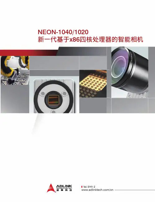
凌华科技ADLINK 智能相机NEON-1040_Datasheet
- 格式:pdf
- 大小:2.13 MB
- 文档页数:8

2014中国机器视觉行业十大知名品牌时间:2015-08-07 10:01:58 来源:作者:乏味机器视觉系统是指通过机器视觉产品(即图像摄取装置,分CMOS和CCD两种)将被摄取目标转换成图像信号,传送给专用的图像处理系统,根据像素分布和亮度、颜色等信息,转变成数字化信号;图像系统对这些信号进行各种运算来抽取目标的特征,进而根据判别的结果来控制现场的设备动作。
在这里盘点一下机器视觉行业知名企业,顺序不代表排名。
1、凌华科技凌华科技(中国)有限公司,是台湾凌华科技集团在中国大陆设立的分公司。
是一家致力于研究、制造基于PC技术的专业计算机、自动化数据量测系统及工业过程自动化控制设备的专业厂商。
几年来,凌华科技以专业的技术为各界的用户提供了高质量、经济化的量测与自动化产品及解决方案。
凌华科技在图像采集卡方面具有强大的科研实力,自行研发制造的产品被广泛应用在SCADA系统、工业、测量、智能机器,智能交通以及现代通讯系统、医疗设备、航天、军工等领域。
2、大恒图像中国大恒(集团)有限公司北京图像视觉技术分公司简称为大恒图像,成立于1991年,总部在北京,是中国科学院下属企业。
大恒图像的技术骨干主要来自中国科学院各研究单位,公司的产品和技术基础来源于中国科学院多年的技术积累,是将高新技术成果转化为产品的高科技企业。
大恒图像自成立之日起,一直坚持走以技术开发为主的发展道路,一直致力于图像视觉领域的研究开发,建立了技工贸一体化的结构,连续十五年被中关村科技园区认定为高新技术企业。
在国内,大恒图像是首屈一指的专业视频图像处理设备供应商,同时也是著名的图像应用系统集成商和解决方案提供商。
3、视觉龙深圳市视觉龙科技有限公司是一家由归国留学人员创办的高科技企业,公司成立于2002年9月,在深圳、常州和嘉兴分别设有公司。
成立以来,公司一直致力于机器视觉产品的应用开发、嵌入式机器视觉系统的研发、生产以及销售。
视觉龙专业涵盖非接触式测量(含机器视觉、位移测量等)、自动化控制、精密机械、电子、工控软件等诸多重要领域。

上海贝尔行业产品手册公司介绍阿尔卡特朗讯是全球领先的通信解决方案供应商,专注于IP网络、超宽带接入和云技术,致力于为全球的运营商、企业和政府机构提供更加灵活、快速、可靠的通信网络。
阿尔卡特朗讯旗下的贝尔实验室是全球最具活力的前沿技术研究机构之一,贡献了一大批奠定现代信息通信基础的创新发明。
贝尔实验室共获得8项诺贝尔奖,拥有14位诺贝尔奖获得者。
最近,阿尔卡特朗讯凭借一系列技术创新,获得国际机构的高度认可。
上海贝尔股份有限公司成立于1984年,是国务院国有资产监督管理委员会的直属企业,也是中国第一家外商投资股份制公司,拥有强大的本土实力和广泛的全球资源。
上海贝尔为运营商、企业和行业客户提供先进的信息通信解决方案和高质量的服务,其产品覆盖有线和无线方案、IP网络、光网络、光接入、云计算、网络核心及应用、网络管理及服务等诸多领域。
上海贝尔拥有贝尔实验室中国研究中心和数个重要的全球研发中心,可全面进入阿尔卡特朗讯全球技术库,开发服务于中国和阿尔卡特朗讯全球客户的独创技术,并且在多项新技术开发中居于主导地位。
上海贝尔拥有技术先进、制造能力达到世界一流水平的生产制造平台,公司销售服务网络遍及全国和海外50多个国家。
今天,上海贝尔已成为集世界一流的生产制造基地,全球重要的研发中心、采购和物流中心、信息服务中心以及上海贝尔大学于一体的阿尔卡特朗讯在全球的旗舰。
目录总体描述 (4)行业解决方案 (5)全业务传送网解决方案 (5)城域网解决方案 (8)骨干网解决方案 (9)数据中心网络解决方案 (10)数据中心互联/出口解决方案 (11)电力数据调度网与综合数据网解决方案 (12)专业DNS_DHCP_IPAM系统解决方案 (13)无源局域网解决方案(POL) (15)端到端L TE解决方案 (17)IMS/NGN解决方案 (19)产品系列 (21)光传送 (21)OTN/WDM 产品-1830 PSS系列产品 (21)PTN-1850 TSS系列产品 (23)MSTP系列产品 (24)微波传输 (25)中短距分组微波-9500 MPR系列产品 (25)长距微波-9600 LSY系列产品 (26)数据承载 (27)骨干/核心路由平台-7950 XRS (27)城域业务路由-7750 SR/7705 SAR (28)MES系列交换机 (30)软件定义网络– Nuage SDN (32)VitalQIP:面向IPv4、IPv6的下一代IP地址管理解决方案 (33)超宽带接入 (34)PON OL T局端设备-7360 ISAM FX (34)丰富的光终端(ONU)系列 (34)LTE无线产品 (37)业务核心网 (38)IMS产品 (38)NGN产品 (38)总体描述通信网的未来将会何去何从?企业期望应对动态的市场和客户需求,实施新的业务策略并开拓新的市场机会,今天的网络已经无法应对日益增长的海量数据,我们需要一个灵活敏捷、伸缩自如的人性化网络,基于IP的网络演进势在必行,而这一切必须以网络为基石。
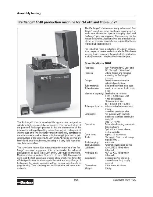
Assembly toolingParflange ® 1040 production machine for O-Lok ® and Triple-Lok ®The Parflange ® 1040 is an orbital flaring machine designed tocold-form high pressure tube connections. The unique feature of the patented Parflange ® process is that the deformation of the tube end is achieved by rolling rather than by just pushing a tool into the tube end. The Parflange ® machine smoothly compresses the tube material and achieves a high strength joint with a pol-ished surface of the tube end. O-Lok ® and SAE flange sleeves are firmly fixed onto the tube end, resulting in a very rigid high-pres-sure tube connection.The 1040 is the heavy-duty, mass production machine of the Par-flange ® machine programme. It is recommended for industrial production of all sizes Triple-Lok ® and O-Lok ® tube connections.Maximum tube capacity is 38 mm/1 1/2 tube O.D. The powerful drive, and the fast, automatic process allow short cycle times for efficient production. Its advantage is the quick and easy change of tooling and the simple operation without manual adjustments or programming. Tube clamping and tool lubrication are done auto-matically.The Parflange ® 1040 comes ready to be used. Par-flange ® tools have to be purchased separately. For each tube dimension, special clamping dies and Parflange ® pins are required. The machine can be moved on wheels. Additionally to the electrical sup-ply, an air pressure connection is required for the in-tegrated lubrication device.For industrial mass production of O-Lok ® connec-tions, a special sleeve feeder is available. This sleeve feeding device increases the productivity, particular-ly of high volume – single tube dimension jobs.Specifications 1040Purpose:180° Flanging for O-Lok ® and 37° Flaring for T riple-Lok ®Process:Orbital flaring and flangingaccording to Parflange ®processDesign:Stand-alone machine forindustrial productionTube material:steel and stainless steel tube Tube diameter:metric: 6 to 38 mm Inch: 1/4 to1 1/2˝Maximum capacity:Steel tube 38 × 5 mm/1 1/2˝ × 0.188 (tube O.D.× wall thickness)Stainless steel tube38 × 4 mm/1 1/2˝ × 0.156Tube specification:fully annealed seamless colddrawnor welded precision tubeLimitations:Not suitable with titaniumstabilised stainless steel tube material(316Ti, 1.4571)Operation:Automatic clamping, automaticflanging/flaringOptional automatic sleeve feeder availableCycle time:approx. 15 to 20 secs.Tools:Flaring pin B30 … and clamp-ing dies M40 …Tool clamping:automatic Tool lubrication:Automatic lubrication device Lubricant:1040LUBSS (filled whendelivered)Hydraulic oil:HLP 23 XXL (filled whendelivered)Installation:electrical power and com-pressed air (6 bar) supplyrequiredDimensions:700 x 840 x 1035 mm Weight:306 kgAssembly toolingApplicationsIndustrial production of T riple-Lok® and O-Lok® connec-tions, High quantity/large diameter assembly projects, Large diameter stainless steel assembly jobs Features, advantages and benefitsof the 10401.Superi or seali ng performance–The patented Par-flange® process achieves a sealing surface of unique surface quality and mechanical strength.2.Superior vibration resistance –Unlike conventionalflaring, the Parflange® process results in a rigid connec-tion of the O-Lok® sleeve on the tube-end. Parflange/ O-Lok® connections perform much better under re-versed bending stress conditions.3.Efficient–The short cycle time and the automaticprocess allow efficient mass production.4.Quality –Tube clamping, tool control and even lubrica-tion is fully automated so that high and consistent qual-ity results are achieved without manual adjustments.5.Low-cost mass producti on–The machine can beequipped with an automated sleeve feeder. The Par-flange® 1040 then is the perfect solution for low-cost mass production.6.Universal –The Parflange® 1040 can do 37° flaring forT riple-Lok® connectors and flange tubes for both O-Lok® fittings (ORFS). Parflange® tools cover metric tube from 6 to 38 mm O.D. and inch tube from 1/4 to 1 1/2˝O.D.7.Heavy duty –The rigid machine design allows use formass production of even large stainless steel tube con-nections.8.Easy to use –The clamping and flanging process isfully automated. Manual tool manipulation is not re-quired.9.Cost saving –Compared to welding or brazing, orbitalflanging is much less time consuming. Special tube preparation and finishing are not necessary. Flanging uses only a fraction of the energy needed for brazing or welding.10.Clean–The Parflange® process is environmentallyclean and safe. As no heat or chemicals are used, haz-ards from fumes or heat do not occur.11.Zinc plated tubing –The Parflange® process allowsthe use of zinc-plated tubing. The cost for cleaning post process plating, or painting can be saved.12.High tool lifetime –The Parflange® 1040 machine isequipped with an automatic lubrication device. The op-erator does not have to lubricate the tools regularly to prevent rapid wear.13.Process/Product concept –Parflange® machines areespecially designed to match O-Lok®, Triple-Lok® and SAE-flange standards. Machine, tools and products are fine-tuned for reliable performance.14.Proven technology–For more than 10 years, hun-dreds of Parflange® machines have operated world-wide under heavy duty workshop conditions.OrderingT ype Order code Parflange® 1040 Basic machineReady to use, including operation manual,filled with hydraulic oil and lubricantWithout Parflange® toolsBasic machine 400 V, 3 Phase, 50 Hz1040-EU400V 1040 promotion leaflet UK4390-P1-UK 1040 promotion leaflet DE4390-P1-DE 1040 operating manual UK/DE/FR/IT4390-B11/ …Feeder for O-Lok® sleeves(not suitable for Triple-Lok®)Sleeve feeder Order codeFor attaching on Parflange® 1040 machineComplete kit including all connectorsand installation/operating manualwithout sleeve feeding rails1040-FEEDER Sleeve feeding rails for 1040 sleeve feederare ordered separately for each tube O.D.6 mm/1/4˝1040/025GS-04 8–10 mm/3/8˝1040/025GS-06 12 mm/1/2˝1040/025GS-08 14–15–16 mm/5/8˝1040/025GS-10 18–20 mm/3/4˝1040/025GS-12 22–25 mm/1˝1040/025GS-16 28–30–32 mm/1 1/4˝1040/025GS-20 35–35 mm/1 1/2˝1040/025GS-24Spare partsT ype Order codeDrive belt1025/028BELT Hydraulic oil filter cartridge G01991Tool lubricant qty: 1L1040/LUBSS Adjustable spray line1040/LMC0102 Tube stop (lever only)1040/0142205 Tube stop kit (complete assembly)1040/0142228Parflange® machines and feeders are shipped in special container which should be kept for all transports to avoid damage.。
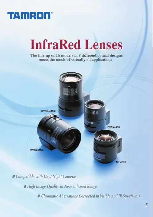
InfraRed Lenses12VG1040ASIR13VG308ASIR13VG2811ASIR13FG28IRCompatible with Day/ Night CamerasHigh Image Quality in Near Infrared RangeChromatic Aberrations Corrected in Visible and IR SpectrumsEManual Manual Manual Manual Manual Manual Manual Manual Manual Manual Manual Manual Manual T ele Wide Focus Zoom IrisModelImage Size OperationWeightMount Focal Length Aperture Range Angular of View (H x V)Manual Iris Auto Iris (DC)3.0-8mm 3.0-8mm 1.0-CloseCS 39g1/31/390.8˚ x 66.6˚90.8˚ x 66.6˚36.2˚ x 27.0˚36.2˚ x 27.0˚1.0-360CS 47gDC-Auto 2.8-11mm 1.4-CloseCS 72g97.4˚ x 72.4˚26.2˚ x 19.7˚1/397.4˚ x 72.4˚26.2˚ x 19.7˚2.8-11mm 1.4-360CS 87gDC-Auto 1/327.5˚ x 20.4˚7.0˚ x 5.2˚10-40mm 1.4-CloseCS 77g1/3Employment of advanced optical designs in all the IR lenses and special glass (LD elements) in the Vari-Focal series has resulted in the elimination of shifts of focus points in both visible and infrared ranges. Rays of light from both spectrums are focused onto the same focal plane, resultingin sharp images. This type of compensation is necessary since IR lenses are ideal not only for Day/ N ight cameras but also for con-ventional B/W cameras that are sensitive to both visible and N ear Infrared light.Aspherical elements are used in Vari-Focal lenses to achieve high contrast and high definition images in all ranges. Additionally, with the rising demand to boost corner resolution due to the increasing popu-larity of digital recorders, the image quality at the corners of the image is enhanced. Tamron’s IR lenses provide the most suitable solution for high quality imaging with digital recorders.The 3.0-8mm lens, the standard Vari-Focal lens, features an F/1.0 maximum aperture to facilitate maximum performance in dimly-lit conditions. Since surveillance may take place in totally dark locations where infrared illumination is used, real 24-hour surveil-lance is now possible.Tamron’s IR lenses are ideal for a variety of applications since the line-up includes 4 different Vari-Focal and 4 Fixed-Focal length lenses. The line-up covers from 2.8mm wideangle (providing 97.4˚ angle of view) to 40mm telephoto (providing 9.2˚ angle of view), in order to meet nearly all applications.*The 10-40mm lens is also compatible with 1/2-inch CCD cameras and is avail-able in manual-iris and DC auto-iris types.A locking mechanism is attached to each control ring. Anchoring the rings in place prevents unwanted shifts in the desired setting after the lens has been mounted.Tamron’s IR lenses use glass having no lead content, and lead-free solder is used in manufacturing. Other environmentally-friendly materials are used as well.Tamron’s special multi-layer coating designed to prevent transmittance fall-off in the infrared range is effectively applied to minimize ghosting and flare caused by back-lighting, thus providing high contrast quality images even in adverse back-lit conditions.A slip mount mechanism designed to allow rotation of the lens after mounting it on the camera is built in for fine-tuning its position. This feature allows the lens’ auto-iris meter on the lower part of the lens to be rotated to the correct position, depending upon the mounting position of the camera.Difference in angles of view with 2.8mm and 40mm Vari-Focal lensComparison of focus conditions with IR and normal lensesTamron IR lensNormal lens[ Images with visible light (under a fluorescent bulb) ][ Images with IR light (850 nm, with a floodlight) ]Compensation of aberration by aspherical elementF/1.0F/1.4f=2.8mm (97.4˚ angle of view) f=40mm (9.2˚ angle of view)10-40mm 1.4-360CS 87gDC-Auto 1/327.5˚ x 20.4˚7.0˚ x 5.2˚10-40mm 1.4-CloseC 77g1/237.5˚ x 27.5˚9.2˚ x 7.0˚10-40mm 1.4-360C 87gDC-Auto 1/237.5˚ x 27.5˚9.2˚ x 7.0˚Advanced Optical Designs Eliminate Shifts of Focus in the Near Infrared Range.Outstanding Image Quality with Aspherical Lens ElementsWide Selection of Lenses in Versatile Ranges for Choosing the Best Angle of ViewWide Dynamic Range of F/1.0 ApertureLocking Mechanism Built into Each RingEnvironmentally-conscious DesignMulti-layer Coating AppliedBuilt-in Slip Mount MechanismIR LensVisible Light LensInfrared lightFocal planeVisible light Infrared lightVisible lightfocal planeIR light focal planeVisible lightBoth IR and visible light come to the same focal plane.Out of focus caused by the focal plane difference. IR lens corrects this difference.Spherical elementAspherical elementImage plane Image planeVari-Focal LensesFixed-Focal LensesWide Focus Zoom IrisModelImage Size Operation WeightMount Focal Length Aperture Range Angular of View (H x V)T eleManual Manual Manual Manual Manual Manual Manual 23The latest optical designs compensate for various aberrations that occur in the visible and near infrared ranges for sharp images in all applications. Tamron’s IR lenses meet the performance characteristics of Day/Night cameras 100%, for real 24-hour surveillance.Manual Iris1/3 2.8mm 1.2-Close CS 36g 1/3 4mm 1.2-Close CS 33g 1/3 6mm 1.2-Close CS 32g 1/3 8mm 1.2-Close CS 33g 1/3 2.8mm 1.2-360 CS 44g 1/3 4mm 1.2-360 CS 40g 1/3 6mm 1.2-360 CS 38g 1/3 8mm 1.2-360 CS 40gModelImage Size WeightMount Focal Length Aperture Range Auto Iris (DC)13VM308ASIR 13VM2811ASIR 13VG1040ASIR 12VG1040ASIR 13FM28IR 13FM04IR 13FM06IR 13FM08IR 13FG28IR 13FG04IR 13FG06IR 13FG08IR 13VG308ASIR 13VM308ASIRTAMRON LENSESPrinted on 100%Specifications subject to change without notice 2004,3Manufacturer of lenses of photographic,Industrial, laboratory, video, and scientific applications.TAMRON CO., LTD.1385, Hasunuma, Minuma-ku, Saitama City, Saitama, Japan TEL +81-48-684-9129 FAX +81-48-683-8594URL http://www.tamron.co.jp e-mail :***************.jpIR4-EG-121-U-0403-0010。
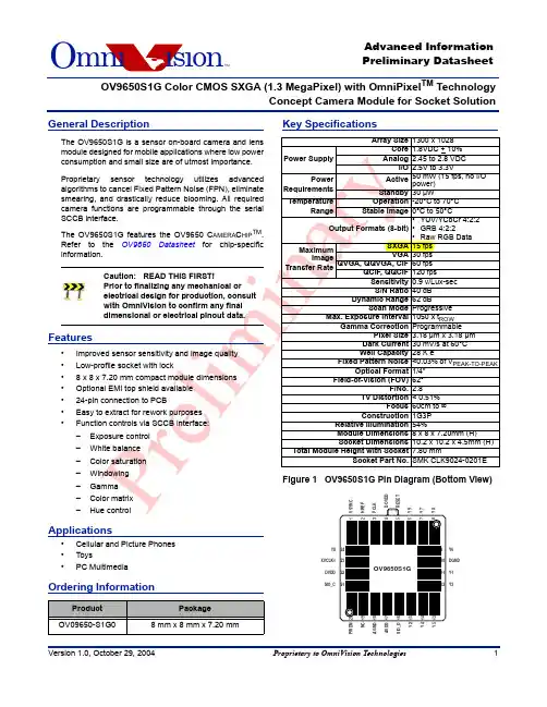
Advanced Information Preliminary DatasheetO mniTMisionOV9650S1G Color CMOS SXGA (1.3 MegaPixel) with OmniPixel TM TechnologyConcept Camera Module for Socket SolutionGeneral DescriptionKey SpecificationsOV9650S1GColor CMOS SXGA (1.3 MegaPixel) OmniPixel™ Camera ModuleO Functional DescriptionFigure 2 shows the functional block diagram of the OV9650S1G Camera Module. The OV9650S1G includes:•1/4"lens •OV9650 C AMERA C HIP image sensor •Socket connectorFigure 2 Functional Block DiagramFunctional DescriptionO Imaging SpecificationsTable 1Sensor Image FunctionsOV9650S1GColor CMOS SXGA (1.3 MegaPixel) OmniPixel™ Camera ModuleOPin DescriptionNOTE:Y[9:2] for 8-bit YUV or RGB (Y9 MSB, Y2 LSB)Y[9:0] for 10-bit RGB (Y9 MSB, Y0 LSB)Table 3Pin DescriptionPin NumberName Pin Type Function/Description01VSYNC Output Vertical sync output 02HREF Output HREF output 03PCLK Output Pixel clock output04DOVDD Power Digital power supply (V DD-IO = 2.5 to 3.3 VDC) for I/O05RESET Function (default = 0)Clears all registers and resets them to their default values. Active high, internal pull-down resistor.06Y9Output Output bit[9] - MSB for 10-bit RGB and 8-bit YUV 07Y7Output Output bit[7]08Y8Output Output bit[8]09Y6Output Output bit[6]10DGND Power Digital ground11Y1Output Output bit[1] - for 10-bit RGB only 12Y3Output Output bit[3]13Y5Output Output bit[5]14Y4Output Output bit[4]15Y2Output Output bit[2] - LSB for 8-bit YUV 16SIO_D I/O SCCB serial interface data I/O17AVDD Power Analog power supply (V DD-A = 2.45 to 2.8 VDC)18AGND Power Analog ground 19NC–Reserved - no connect20PWDNFunction (default = 0)Power Down Mode Selection - active high, internal pull-down resistor.0:Normal mode1:Power down mode 21SIO_C Input SCCB serial interface clock input22DVDD Power Power supply (V DD-C = 1.8 VDC + 10%) for digital core logic 23XVCLK1Input Crystal clock input24Y0OutputOutput bit[0] - LSB for 10-bit RGB onlyElectrical CharacteristicsOElectrical CharacteristicsNOTE:Exceeding the Absolute Maximum ratings shown above invalidates all AC and DC electrical specifications and may result in permanent device damage.Table 4Absolute Maximum RatingsAmbient Storage Temperature-40ºC to +95ºCSupply Voltages (with respect to Ground)V DD-A4.5 V V DD-C 3 V V DD-IO4.5 VAll Input/Output Voltages (with respect to Ground)-0.3V to V DD-IO +1V Lead Temperature, Surface-mount process +230ºC ESD Rating, Human Body model 2000VTable 5DC Characteristics (-20°C < T A < 70°C)Symbol ParameterConditionMin Typ Max Unit V DD-A DC supply voltage – Analog – 2.45 2.5 2.8V V DD-C DC supply voltage – Core – 1.62 1.8 1.98V V DD-IO DC supply voltage – I/O power – 2.25– 3.6V I DDA Active (Operating) Current See Note a a. V DD-A = 2.5V, V DD-C = 1.8V, V DD-IO = 3.0VI DDA = ∑{I DD-IO + I DD-C + I DD-A }, f CLK = 24MHz at 7.5 fps YUV output, no I/O loading20mA I DDS-SCCB Standby Current See Note b b. V DD-A = 2.5V, V DD-C = 1.8V, V DD-IO = 3.0VI DDS:SCCB refers to a SCCB-initiated Standby, while I DDS:PWDN refers to a PWDN pin-initiated Standby 1mA I DDS-PWDN Standby Current 10µA V IH Input voltage HIGH CMOS0.7 x V DD-IOV V IL Input voltage LOW 0.3 x V DD-IOV V OH Output voltage HIGH CMOS0.9 x V DD-IOV V OL Output voltage LOW 0.1 x V DD-IOV I OH Output current HIGH See Note cc.Standard Output Loading = 25pF, 1.2K Ω8mA I OL Output current LOW 15mA I LInput/Output LeakageGND to V DD-IO ± 1µAOV9650S1G Color CMOS SXGA (1.3 MegaPixel) OmniPixel™ Camera Module OTable 6 Functional and AC Characteristics (-20°C < T A < 70°C)Symbol Parameter Min Typ Max Unit Functional CharacteristicsA/D Differential Non-Linearity+ 1/2LSBA/D Integral Non-Linearity+1LSBAGC Range18dBRed/Blue Adjustment Range12dB Inputs (PWDN, CLK, RESET)f CLK Input Clock Frequency102448MHzt CLK Input Clock Period2142100ns t CLK:DC Clock Duty Cycle455055% t S:RESET Setting time after software/hardware reset1ms t S:REG Settling time for register change (10 frames required)300ms SCCB Timing (see Figure4)f SIO_C Clock Frequency400KHzt LOW Clock Low Period 1.3µs t HIGH Clock High Period600ns t AA SIO_C low to Data Out valid100900ns t BUF Bus free time before new START 1.3µs t HD:STA START condition Hold time600ns t SU:STA START condition Setup time600ns t HD:DAT Data-in Hold time0µs t SU:DAT Data-in Setup time100ns t SU:STO STOP condition Setup time600ns t R, t F SCCB Rise/Fall times300ns t DH Data-out Hold time50ns Outputs (VSYNC, HREF, PCLK, and Y[9:0] (see Figure5, Figure6, Figure7, Figure8, Figure10, and Figure11) t PDV PCLK[↓] to Data-out Valid5ns t SU Y[9:0] Setup time15ns t HD Y[9:0] Hold time8ns t PHH PCLK[↓] to HREF[↑]05ns t PHL PCLK[↓] to HREF[↓]05nsAC Conditions:• V DD: V DD-C = 1.8V, V DD-A = 2.5V, V DD-IO = 3.0V • Rise/Fall Times: I/O: 5ns, MaximumSCCB: 300ns, Maximum • Input Capacitance: 10pf• Output Loading: 25pF, 1.2KΩ to 3V• f CLK: 24MHzTiming SpecificationsOTiming SpecificationsFigure 4 SCCB Timing DiagramOV9650S1G Color CMOS SXGA (1.3 MegaPixel) OmniPixel™ Camera Module OFigure 7 VGA Frame TimingTiming SpecificationsOFigure 10 CIF Frame TimingOV9650S1G Color CMOS SXGA (1.3 MegaPixel) OmniPixel™ Camera Module OFigure 13 RGB 565 Output Timing DiagramRegister Set Table7 shows detailed descriptions of the Device Control registers. The device slave addresses for the OV9650S1G are 60 for write and 61 for read.Table 7 Device Control Register ListAddress (Hex)RegisterNameDefault(Hex)R/W Description00GAIN00RW AGC[7:0] – Gain control gain setting •Range: [00] to [FF]01BLUE80RW AWB – Blue channel gain setting •Range: [00] to [FF]02RED80RW AWB – Red channel gain setting •Range: [00] to [FF]03VREF12RW Vertical Frame ControlBit[7:6]:AGC[9:8] (see register GAIN for AGC[7:0])Bit[5:3]:VREF end low 3 bits (high 8 bits at VSTOP[7:0] Bit[2:0]:VREF start low 3 bits (high 8 bits at VSTRT[7:0]04COM100RW Common Control 1Bit[7]:ReservedBit[6]:CCIR656 formatBit[5]:QQVGA or QQCIF format. Effective only when QVGA or QCIF output is selected (register bit COM7[4]) and relatedHREF skip mode based on format is selected (registerCOM1[3:2])Bit[4]:ReservedBit[3:2]:HREF skip option00:No skip01:YUV/RGB skip every other row for YUV/RGB, skip 2rows for every 4 rows for Raw data1x:Skip 3 rows for every 4 rows for YUV/RGB, skip 6 rowsfor every 8 rows for Raw dataBit[1:0]:AEC low 2 LSB (see registers AECHM for AEC[15:10] and AECH for AEC[9:2])05BAVE00RW U/B Average LevelAutomatically updated based on chip output format06GEAVE00RW Y/Ge Average LevelAutomatically updated based on chip output format07RSVD00–Reserved08RAVE00RW V/R Average LevelAutomatically updated based on chip output format09COM201RW Common Control 2Bit[7:5]:ReservedBit[4]:Soft sleep modeBit[3:2]:ReservedBit[1:0]:Output drive capability00:1x01:2x10:2x11:4x0A PID96R Product ID Number MSB (Read only) 0B VER50R Product ID Number LSB (Read only)0C COM300RW Common Control 3Bit[7]:ReservedBit[6]:Output data MSB and LSB swapBit[5:4]:ReservedBit[3]:Pin selection1:Change RESET pin to EXPST_B (frame exposuremode timing) and change PWDN pin to FREX (frameexposure enable)Bit[2]:VarioPixel for VGA and CIFBit[1]:ReservedBit[0]:Single frame output (used for Frame Exposure mode only)0D COM400RW Common Control 4Bit[7]:VarioPixel for QVGA, QCIF, QQVGA, and QQCIFBit[6]:ReservedBit[5]:Pixels for sub-sampling mode0:Get average neighbor pixel in sub-sampling mode1:Get sum instead of average neghbor pixel insub-sampling modeBit[4:3]:ReservedBit[2]:Tri-state option for output clock at power-down period 0:Tri-state at this period1:No tri-state at this periodBit[1]:Tri-state option for output data at power-down period 0:Tri-state at this period1:No tri-state at this periodBit[0]:Reserved(Hex)Name(Hex)R/W Description0E COM501RW Common Control 5Bit[7]:System clock selection. If the system clock is 48 MHz, this bit should be set to high to get 15 fps for YUV or RGB Bit[6:5]:ReservedBit[4]:Slam mode enable0:Master mode1:Slam mode (used for slave mode)Bit[3]:ADC offset manual control0:Offset is controlled automatically1:Register OFON[7:4] can enable ADC offset addition Bit[2:1]:ReservedBit[0]:Exposure step can be set longer than VSYNC time1:In Normal mode, AEC changes by 1/16 and in Fastmode, AEC changes by double0F COM643RW Common Control 6Bit[7]:Output of optical black line option0:Disable HREF at optical black1:Enable HREF at optical black Bit[6:5]:ReservedBit[4]:HREF is high from optical black lineBit[3]:Enable bias for ADBLCBit[2]:ADBLC offset0:Use 4-channel ADBLC1:Use 2-channel ADBLCBit[1]:Reset all timing when format changes Bit[0]:Enable ADBLC option10AECH40RW Exposure ValueBit[7:0]:AEC[9:2] (see registers AECHM for AEC[15:10] and COM1 for AEC[1:0])11CLKRC00RW Data Format and Internal ClockBit[7]:Digital PLL option0:Disable double clock option, meaning the maximumPCLK can be as high as half input clock1:Enable double clock option, meaning the maximumPCLK can be as high as input clockBit[6]:Use external clock directly (no clock pre-scale available) Bit[5:0]:Internal clock pre-scalarF(internal clock) = F(input clock)/(Bit[5:0]+1)•Range: [0 0000] to [1 1111](Hex)Name(Hex)R/W Description12COM700RW Common Control 7Bit[7]:SCCB Register Reset0:No change1:Resets all registers to default valuesBit[6]:Output format - VGA selectionBit[5]:Output format - CIF selectionBit[4]:Output format - QVGA selectionBit[3]:Output format - QCIF selectionBit[2]:Output format - RGB selectionBit[1]:ReservedBit[0]:Output format - Raw RGB (COM7[2] must be set high)13COM88F RW Common Control 8Bit[7]:Enable fast AGC/AEC algorithmBit[6]:AEC - Step size limit (used only in fast condition and COM5[0] is low)0:Fast condition change maximum step is VSYNC1:Unlimited step sizeBit[5]:Banding filter ON/OFFBit[4]:ReservedBit[3]:Enable AEC time can be less than 1 line optionBit[2]:AGC EnableBit[1]:AWB EnableBit[0]:AEC Enable14COM94A RW Common Control 9Bit[7]:ReservedBit[6:4]:Automatic Gain Ceiling - maximum AGC value000:2x001:4x010:8x011:16x100:32x101:64x110:128xBit[3]:Exposure timing can be less than limit of banding filter when light is too strongBit[2]:Data format - VSYNC drop option0:VSYNC always exists1:VSYNC will drop when frame data drops Bit[1]:Enable drop frame when AEC step is larger than VSYNC Bit[0]:Freeze AGC/AEC(Hex)Name(Hex)R/W Description21GBOS80RW Gb channel ADBLC resultBit[7]:Offset adjustment sign0:Add offset1:Subtract offsetBit[6:0]:Offset value of 10-bit range22GROS80RW Gr channel ADBLC resultBit[7]:Offset adjustment sign0:Add offset1:Subtract offsetBit[6:0]:Offset value of 10-bit range23ROS80RW R channel ADBLC resultBit[7]:Offset adjustment sign0:Add offset1:Subtract offsetBit[6:0]:Offset value of 10-bit range24AEW78RW AGC/AEC - Stable Operating Region (Upper Limit) 25AEB68RW AGC/AEC - Stable Operating Region (Lower Limit)26VPT D4RW AGC/AEC Fast Mode Operating Region Bit[7:4]:Upper limit of 4 MSBBit[3:0]:Lower limit of 4 LSB27BBIAS80RW B Channel Signal Output Bias (effective only when COM6[0] = 1)Bit[7]:Bias adjustment sign0:Add bias1:Subtract biasBit[6:0]:Bias value of 10-bit range28GbBIAS80RW Gb Channel Signal Output Bias (effective only when COM6[0] = 1) Bit[7]:Bias adjustment sign0:Add bias1:Subtract biasBit[6:0]:Bias value of 10-bit range29Gr_COM00RW Analog BLC and Regulator Control Bit[7:6]:ReservedBit[5]:Bypass Analog BLCBit[4]:Bypass regulatorBit[3:0]:Reserved2A EXHCH00RW Dummy Pixel Insert MSBBit[7:4]: 4 MSB for dummy pixel insert in horizontal direction Bit[3:2]:HSYNC falling edge delay 2 MSBBit[1:0]:HSYNC rising edge delay 2 MSB2B EXHCL00RW Dummy Pixel Insert LSB8 LSB for dummy pixel insert in horizontal direction(Hex)Name(Hex)R/W Description2C RBIAS80RW R Channel Signal Output Bias (effective only when COM6[0] = 1) Bit[7]:Bias adjustment sign0:Add bias1:Subtract biasBit[6:0]:Bias value of 10-bit range2D ADVFL00RW LSB of insert dummy lines in vertical direction (1 bit equals 1 line) 2E ADVFH00RW MSB of insert dummy lines in vertical direction2F YAVE00RW Y/G Channel Average Value30HSYST08RW HSYNC Rising Edge Delay (low 8 bits)31HSYEN30RW HSYNC Falling Edge Delay (low 8 bits)32HREF A4RW HREF ControlBit[7:6]:HREF edge offset to data outputBit[5:3]:HREF end 3 LSB (high 8 MSB at register HSTOP) Bit[2:0]:HREF start 3 LSB (high 8 MSB at register HSTART)33CHLF00RW Bit[7:0]:Reserved 34ARBLM03RW Bit[7:0]:Reserved 35-36RSVD XX–Reserved37ADC04RW Bit[7:0]:Reserved 38ACOM12RW Bit[7:0]:Reserved39OFON00RW Bit[7:4]:ReservedBit[3]:Line buffer power down - must be set to "1" before chip power downBit[2:0]:Reserved3A TSLB0C RW Line Buffer Test OptionBit[7:6]:ReservedBit[5]:Bit-wise reverseBit[4]:UV output value0:Use normal UV output1:Use fixed UV value set in registers MANU and MANVas UV output instead of chip outputBit[3]:Output sequence is Y U Y V instead of U Y V YBit[2]:Output sequence is Y V Y U instead of Y U Y VBit[1]:ReservedBit[0]:Digital BLC(Hex)Name(Hex)R/W Description3B COM1100RW Common Control 11Bit[7]:Night mode0:Night mode disable1:Frame rate will adjust based on COM11[6:5] beforeAGC gain increases more than 2. Also,ADVFL andADVFL will be automatically updated.Bit[6:5]:Night mode insert frame option00:Normal frame rate01:1/2 frame rate10:1/4 frame rate11:1/8 frame rateBit[4:3]:Average calculation window option00:Use full frame01:Use half frame10:Use quarter frame11:Use lower two-thirdsBit[2:1]:ReservedBit[0]:Manual banding filter mode3C COM1240RW Common Control 12Bit[7]:HREF option0:No HREF when VREF is low1:Always has HREFBit[6:3]:ReservedBit[2]:Enable YUV averageBit[1:0]:Reserved3D COM1399RW Common Control 13Bit[7:6]:Gamma selection for signal00:No gamma function01:Gamma used for Y channel only10:Gamma used for Raw data before interpolation11:Not allowedBit[5]:ReservedBit[4]:Enable color matrix for RGB or YUVBit[3]:Enable Y channel delay option0:Delay UV channel1:Delay Y channelBit[2:0]:Output Y/UV delay3E COM140E RW Common Control 14Bit[7:2]:ReservedBit[1]:Enable edge enhancement for YUV output (effective only for YUV/RGB, no use for Raw data)Bit[0]:Edge enhancement option0:Edge enhancement factor = EDGE[3:0]1:Edge enhancement factor = 2 x EDGE[3:0](Hex)Name(Hex)R/W Description3F EDGE88RW Edge Enhancement AdjustmentBit[7:4]:Edge enhancement threshold[3:0](see register COM22[7:6} for Edge threshold[5:4]) Bit[3:0]:Edge enhancement factor40COM15C0RW Common Control 15Bit[7:6]:Data format - output full range enable0x:Output range: [10] to [F0]10:Output range: [01] to [FE]11:Output range: [00] to [FF]Bit[5:4]:RGB 555/565 option (must set COM7[2] high) x0:Normal RGB output01:RGB 56511:RGB 555Bit[3]:Swap R/B in RGB565/RGB555 formatBit[2:0]:Reserved41COM1610RW Common Control 16Bit[7:2]:ReservedBit[1]:Color matrix coefficient double option Bit[0]:Reserved42COM1708RW Common Control 17Bit[7:5]:ReservedBit[4]:Edge enhancement optionBit[3]:ReservedBit[2]:Select single frame outBit[1]:Tri-state outputBit[0]:Reserved43-4E RSVD XX–Reserved4F MTX158RW Matrix Coefficient 1 50MTX248RW Matrix Coefficient 2 51MTX310RW Matrix Coefficient 3 52MTX428RW Matrix Coefficient 4 53MTX548RW Matrix Coefficient 5 54MTX670RW Matrix Coefficient 6 55MTX740RW Matrix Coefficient 7 56MTX840RW Matrix Coefficient 8 57MTX940RW Matrix Coefficient 958MTXS0F RW Matrix Coefficient Sign for coefficient 9 to 2 0:Plus1:Minus59-61RSVD XX–Reserved(Hex)Name(Hex)R/W Description62LCC100RW Lens Correction Option 163LCC200RW Lens Correction Option 264LCC310RW Lens Correction Option 365LCC480RW Lens Correction Option 466LCC500RW Lens Correction Control67MANU80RW Manual U Value (effective only when register TSLB[4] is high) 68MANV80RW Manual V Value (effective only when register TSLB[4] is high)69HV00RW Manual Banding Filter MSBBit[7:1]:ReservedBit[0]:Matrix coefficient 1 sign6A MBD00RW LSB of Banding Filter Value (effective only when COM11[0] is high). 6B DBLV0A RW Bit[7:0]:Reserved6C-7B GSP XX RW Gamma curve7C-8A GST XX RW Gamma curve8B COM2104RW Common Control 21Bit[7:4]:ReservedBit[3]:VGA option - use VGA window modeBit[2]:ReservedBit[1]:Digital BLC optionBit[0]:UV channel uses sum or average of neighbor pixel in sub-sampling mode8C COM2200RW Common Control 22Bit[7:6]:Edge enhancement threshold[5:4](see register EDGE[7:4} for Edge threshold[3:0]) Bit[5]:De-noise enableBit[4:2]:ReservedBit[1]:White-pixel erase enableBit[0]:White-pixel erase option8D COM2300RW Common Control 23Bit[7:5]:ReservedBit[4]:Color bar test modeBit[3:2]:ReservedBit[1]:Digital AWB enableBit[0]:Reserved8E COM2400RW Common Control 24Bit[7:0]:Reserved(Hex)Name(Hex)R/W DescriptionRegister SetO8F DBLC10F RWDigital BLC Offset SignBit[7:4]:ReservedBit[3]:Digital BLC B offset sign Bit[2]:Digital BLC R offset sign Bit[1]:Digital BLC Gb offset sign Bit[0]:Digital BLC Gr offset sign90DBLC_B 00RWDigital BLC B Channel Offset ValueBit[7:0]:Digital BLC B channel offset value91DBLC_R 00RWDigital BLC R Channel Offset ValueBit[7:0]:Digital BLC R channel offset value92DM_LNL 00RWDummy Line low 8 bitsBit[7:0]:Control insert Dummy line[7:0]93DM_LNH 00RW Dummy Line high 8 bitsBit[7:0]:Control insert Dummy line[15:8]94-9C RSVD XX –Reserved9D LCCFB 00RW Lens Correction B Channel Control 9E LCCFR 00RW Lens Correction R Channel Control 9FDBLC_Gb00RWDigital BLC Gb Channel Offset ValueBit[7:0]:Digital BLC Gb channel offset value A0DBLC_Gr 00RWDigital BLC Gr Channel Offset ValueBit[7:0]:Digital BLC Gr channel offset valueA1AECHM40RWExposure Value - AEC MSB 5 bitsBit[7:6]:ReservedBit[5:0]:AEC[15:10] (see registers AECH for AEC[9:2] and COM1 for AEC[1:0])A2-A3RSVD XX –ReservedA4COM2500RWCommon Control 25Bit[7:0]:ReservedA5COM2600RWCommon Control 26Bit[7:0]:ReservedA6G_GAIN 80RWGreen Gain OptionBit[7:0]:Green gain when using digital AWBA7VGA_ST 14RW Vertical Start Point for VGABit[7:0]:Define vertical start point in VGA sub-windowing modeA8-AAACOMXX–ReservedNOTE: All other registers are factory-reserved. Please contact OmniVision Technologies for reference register settings.Table 7Device Control Register List (Continued)Address (Hex)Register NameDefault (Hex)R/WDescription8.008.00AA1.50s4.507.20s6.20SECTION A-ALensLens HolderKey for image orientationPCBImage PlaneImage Sensor6.606.6010.20Package SpecificationsOMechanical SpecificationsConnector InformationThe OV9650S1G uses a 24-pin socket connector. Table 9 shows a listing of some recommended connectors.Optical SpecificationsTable 8Mechanical DimensionsParameterSpecification CommentsSensor 5.1 mm x 5.72 mm CMOS in housingLensGlass/Plastic Connection Type 10.2 x 10.2 x 4.5 mm SMK socket (consult OmniVision for details)Module Housing8 mm x 8 mm x 7.20 mmTable 9 Recommended ConnectorsManufacturerPart No.DescriptionSMKCLE9024-0201E CLE9024-0301F T-54-10499T-347379-JIGUSocket connector Shield case (optional)Socket without locking mechanism (for testing purposes)Module extraction jigTable 10Optical SpecificationsParameterSpecification CommentsLens Elements Glass/Plastic Hybrid1 glass, 3 plastic (aspheric) fixed focusViewing Angle 60° diagonal Focal Length 4.7 mm F Number 2.8Focus Range 30 cm → ∞FilterIR cut IncludedMount Description M7 x 0.35P TV Distortion 0.51%Focus AdjustmentFixed80 cmOV9650S1GColor CMOS SXGA (1.3 MegaPixel) OmniPixel™ Camera ModuleOHandling Precautions•DO NOT try to open the unit enclosure as there is no user-serviceable component inside.•To prevent damage to the camera module by electrostatic discharge, handle the camera module ONLY after discharging ALL static electricity from yourself and ensuring a static-free environment for the camera module.•DO NOT touch the top surface of the lens.•DO NOT press down on the lens.•DO NOT try to focus the lens.•DO NOT put the camera module in a dusty environment.•To reduce the risk of electrical shock and damage to the camera module, turn OFF the power before connect and disconnect the camera module.•DO NOT drop the camera module more than 60 cm onto any hard surface.•To prevent fire or shock hazard, DO NOT expose camera module to rain or moisture.•DO NOT expose camera module to direct sunlight.•DO NOT put camera module in a high temperature environment.•DO NOT use liquid or aerosol cleaners to clean the lens.•DO NOT make any changes or modifications to camera module.•DO NOT subject camera module to strong electromagnetic field.•DO NOT subject the camera module to excessive vibration or shock.WARNING: READ THIS FIRST!Prior to handling any OmniVision camera module, read the following precautions.Handling PrecautionsONote:•All information shown herein is current as of the revision and publication date. Please refer to the OmniVision web site ( ) to obtain the current versions of all documentation.•OmniVision Technologies, Inc. reserves the right to make changes to their products or todiscontinue any product or service without further notice (It is advisable to obtain current product documentation prior to placing orders).•Reproduction of information in OmniVision product documentation and specifications is permissible only if reproduction is without alteration and is accompanied by all associated warranties, conditions, limitations and notices. In such cases, OmniVision is not responsible or liable for any information reproduced.•This document is provided with no warranties whatsoever, including any warranty of merchantability, non-infringement, fitness for any particular purpose, or any warranty otherwise arising out of any proposal, specification or sample. Furthermore, OmniVision Technologies Inc. disclaims all liability, including liability for infringement of any proprietary rights, relating to use of information in this document. No license, expressed or implied, by estoppels or otherwise, to any intellectual property rights is granted herein.•‘OmniVision’, ‘CameraChip’, and ’OmniPixel’ are trademarks of OmniVision Technologies, Inc. All other trade, product or service names referenced in this release may be trademarks orregistered trademarks of their respective holders. Third-party brands, names, and trademarks are the property of their respective owners.For further information, please feel free to contact OmniVision at info@ .OmniVision Technologies, Inc.1341 Orleans Drive Sunnyvale, CA USA (408) 542-3000OV9650S1G Color CMOS SXGA (1.3 MegaPixel) OmniPixel™ Camera Module O。
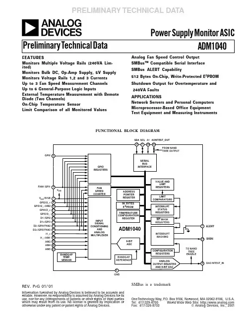
=Power Supply Monitor ASICADM1040FEATURESMonitors Multiple Volta ge Ra ils (240VA Lim-ited)Monitors Bulk DC, Op-Amp Supply, 5V Supply Monitors Volta ge Ra ils 1,2 a nd 3 Currents Up to 3 Fa n Speed Mea surement Cha nnels Up to 6 General-Purpose Logic InputsExterna l Tempera ture Mea surement with Remote Diode (Two Channels)On-Chip Tempera ture SensorLimit Compa rison of a ll Monitored Va luesFUNCTIONAL BLOCK DIAGRAMREV. PrG 01/'01Information furnished by Analog Devices is believed to be accurate and reliable. However, no responsibility is assumed by Analog Devices for its use, nor for any infringements of patents or other rights of third parties which may result from its use. No license is granted by implication or otherwise under any patent or patent rights of Analog Devices.One Technology Way, P .O. Box 9106, Norwood, MA 02062-9106, U.S.A.Tel: 617/329-4700World Wide Web Site: Fax: 617/326-8703© Analog Devices, Inc., 2001Preliminary T echnical D ataSMBus is a trademarkAna log Fa n Speed Control Output SMBus TM Compa tible Seria l Interfa ce SMBus ALERT Ca pa bility512 Bytes On-Chip, Write-Protected E 2PROM Shutdown Output for Overtemperature and 240VA FaultsAPPLICATIONSNetwork Servers and Personal Computers Microprocessor-Ba sed Office Equipment Test Equipment and Measuring InstrumentsPRELIMINARY TECHNICAL DATAGNDSCL SDA A0/NTEST_OUT V DD /5VSBGPI3/I2_-/AIN2D1-/GPI2D1+/GPI3D2-/GPI4/FAN2D2+/GPI5/FAN3I1_-/AIN1AIN3AIN4AIN5GPI0FAN1/GPI1ALERTA1SHDNDAC/NTEST_IN元器件交易网。

APDS-9002Miniature Surface-Mount Ambient Light Photo SensorData SheetDescriptionThe APDS-9002 is a low-cost analog-output ambient light photo sensor in lowest cost miniature chipLED lead-free surface mount package. It consists of a spectrally suited phototransistor, which peaks in human luminosity curve. Hence, it provides an excellent responsivity that is close to the response of human eyes, as shown in Figure 2. It provides a design-alternative to the HSDL-9000 digital-output ambient light photo sensor is suitable for portable applications with its ultra small package design.The APDS-9002 is ideal for applications in which the measurement of ambient light is used to control display backlighting. Mobile appliances such as the mobile phones and PDAs that draw heavy current from display backlighting will benefi t from incorporating these photo sensor products in their designs by reducing power con-sumption signifi cantly.Features∙ Excellent responsivity which peaks in the human luminosity curve– Close responsivity to the human eye∙ Miniature chipLED lead-free surface-mount package – Height – 0.80 mm– Width – 2.00 mm– Depth – 1.25 mm∙ Good output linearity across wide illumination range∙ Low sensitivity variation across various light sources∙ Guaranteed temperature performance: -40° C to 85° C∙ VCC supply 2.4 to 5.5 V∙ L ead-free packageApplications∙ Detection of ambient light to control display back-lighting– Mobile devices – mobile phones, PDAs– Computing devices – notebooks, webpads– Consumer devices – TVs, video cameras, digital still cameras∙ Automatic residential and commercial lighting management∙ Electronic signs and signals∙ Daylight and artifi cial light exposed devicesI/O Pins Confi guration TablePin Symbol Description1IOUTI OUT 2 VCC V CC 3 VCC V CC4 NCNo ConnectApplication Support InformationThe Application Engineering Group is available to assist you with the application design associated with APDS-9002 ambient light photo sensor module. You can contact them through your local sales representatives for additional details.Ordering InformationPart NumberPackaging TypePackageQuantityAPDS-9002-021Tape and Reel4-pins Chipled package2500Typical Application CircuitFigure 1 TableComponentRecommended Application Circuit ComponentsR LOAD1 kFigure 1. Typical application circuit for APDS-9002.CAUTION: It is advised that normal static precautions be taken in handling and assemblyof this component to prevent damage and/or degradation which may be induced by ESD.N O R M A L I Z E D R E S P O N S I V I T Y0WAVELENGTH (nm)0.50.10.41.11.00.70.20.30.60.90.8Figure 2. Relative spectral response vs. wavelength.Absolute Maximum RatingsFor implementations where case to ambient thermal resistance is ≤ 50°C/WParameter Symbol Min. Max. UnitsStorage Temperature T S -40 85 °C Operating Temperature T A -4085 °C Supply VoltageV CC2.4 5.5 V Recommended Operating ConditionsParameter Symbol Min. Max. Units ConditionsOperating Temperature T A -40 85 °C Supply VoltageV CC2.4 5.5 VElectrical & Optical Specifi cations (T A = 25° C)Parameter Symbol Min. Typ. Max. Units ConditionsPhoto Current (I) I_PH1 10 20 33 μA V CC = 3.0 V, Lux = 10[2]Photo Current (II) I_PH2136 250 410 μAV CC = 3.0 V, Lux = 100[2]Photo Current (III) I_PH3 –300 – μAV CC = 3.0 V, Lux = 100[1]Dark Current I_DARK – 50 160 nA V CC = 3.0 V, Lux = 0Light Current Ratio I_PH3 / I_PH2– 1.2 – – –Rise Time T_RISE – 0.95 2 ms V CC = 3.0 V, Lux = 100, Rload = 1 k Ω[3]Fall TimeT_FALL – 0.8 2 ms V CC = 3.0 V, Lux = 100, R load = 1 k Ω[3]Notes:1. Illuminance by CIE standard light source (incandescent lamp).2. Fluorescent light is used as light source. White LED is substituted in mass production.3. White LED is used as light source.Light Measurement Circuit and WaveformsLOADI_pulseGNDPIN 2: VCCPIN 3: VCCFigure 3. Photocurrent vs. luminence (V CC = 3 V, T A = 25° C).Figure 4. Normalized photocurrent vs. temperature (V CC = 3 V, 100 LUX).Figure 5. Normalized photocurrent vs. angle (V CC = 3 V, T A = 25° C).Figure 6. Output voltage vs. luminance at diff erent load resistor.Figure 7. Fall time vs. R LOAD .Figure 8. Rise time vs. R LOAD .LUXP H O T O C U R R E N T (A )0.010.0010.00010.00001TEMPERATURE (C)N O R M A L I Z E D P HO T O CUR R E N TANGLEN O R M A L I Z E D P H O T O C U R R E N T1.21.000.20.40.60.8LUMINANCE, Ev (LUX)O U T P U T V O L T A G E , V O U T (V )1010.010.0010.1R LOAD (:)F A L L T I M E (s e c )000.0E+0200.0E-6400.0E-6600.0E-6800.0E-61.0E-31.2E-31.4E-3R LOAD (:)T r i s e (s e c )000.0E+0200.0E-6400.0E-6600.0E-6800.0E-61.0E-31.2E-31.6E-31.4E-31.8E-3MATERIAL OF COVER TAPE: PVCMETHOD OF COVER: HEAT SENSITIVE ADHESIVEUNIT: mm"B""C"17875± 0.50DETAIL A±Baking ConditionsIf the parts are not stored in dry conditions, they must be baked before refl ow to prevent damage to the parts.Package Temp. TimeIn Reels 60° C 20 hours In Bulk125° C5 hoursMoisture Proof PackagingAll APDS-9002 options are shipped in moisture proof package. Once opened, moisture absorption begins. This part is compliant to JEDEC Level 4.Recommended Refl ow Profi let-TIME (SECONDS)T – T E M P E R A T U R E – (°C )23020016012080180220255P1HEAT UPP2SOLDER PASTE DRY P3SOLDERREFLOWP4COOL DOWN25Process ZoneSymbol∆T Maximum ∆T/∆TimeHeat Up P1, R1 25° C to 160° C 4°C/s Solder Paste Dry P2, R2 160° C to 200° C0.5°C/s Solder Refl ow P3, R3 200° C to 255° C (260° C at 10 seconds max.) 4°C/s P3, R4 255° C to 200° C -6°C/s Cool DownP4, R5200° C to 25° C-6°C/sThe refl ow profi le is a straightline representation of a nominal temperature profi le for a convective refl ow solder process. The temperature profi le is divided into four process zones, each with diff erent ∆T/∆time temperature change rates. The ∆T/∆time rates are detailed in the above table. The temperatures are measured at the component to printed circuit board connections.In process zone P1, the PC board and APDS-9002 castella-tion pins are heated to a temperature of 160° C to activate the fl ux in the solder paste. The temperature ramp up rate, R1, is limited to 4° C per second to allow for even heating of both the PC board and APDS-9002 castellations.Process zone P2 should be of suffi cient time duration (60 to120 seconds) to dry the solder paste. The temperature is raised to a level just below the liquidus point of the solder, usually 200° C (392° F).Process zone P3 is the solder refl ow zone. In zone P3, thetemperature is quickly raised above the liquidus point of solder to 255° C (491° F) for optimum results. The dwell time above the liquidus point of solder should be between 20 and 60 seconds. It usually takes about 20 seconds to assure proper coalescing of the solder balls into liquid solder and the formation of good solder connections. Beyond a dwell time of 60 seconds, the intermetallic growth within the solder connections becomes excessive, resulting in the formation of weak and unreliable connec-tions. The temperature is then rapidly reduced to a point below the solidus temperature of the solder, usually 200° C (392° F), to allow the solder within the connections to freeze solid.Process zone P4 is the cool down after solder freeze. Thecool down rate, R5, from the liquidus point of the solder to 25° C (77° F) should not exceed 6° C per second maximum. This limitation is necessary to allow the PC board and APDS-9002 castellations to change dimensions evenly, putting minimal stresses on the APDS-9002.Appendix A: SMT Assembly Application NoteAvago APDS-9002: Miniature Surface-Mount Ambient Light SensorFigure 9. Stencil and PCBA.1.1 Recommended Land Pattern0.45SOLDER MASKFigure 10. Solder stencil aperture.Figure 11. Adjacent land keepout and solder mask areas.1.2 Recommended Metal Solder Stencil ApertureIt is recommended that a 0.10 mm (0.004 inches) thick stencil be used for solder paste printing. Aperture opening for shield pad is 0.6 mm x 0.6 mm. This is to ensure adequate printed solder paste volume and no shorting.1.3 Adjacent Land Keepout and Solder Mask AreasAdjacent land keep-out is the maximum space occupied by the unit relative to the land pattern. There should be no other SMD components within this area.The minimum solder resist strip width required to avoid solder bridging adjacent pads is 0.2 mm.Note: Wet/L iquid Photo-Imageable solder resist/mask is recommended.Appendix B: Optical Window Design for APDS-90022.0 Optical Window DimensionsTo ensure that the performance of the APDS-9002 will not be aff ected by improper window design, there are some constraints on the dimensions and design of the window. There is a constraint on the minimum size of the window, which is placed in front of the photo light sensor, so that it will not aff ect the angular response of the APDS-9002. This minimum dimension that is recommended will ensure at least a ±35° light reception cone.If a smaller window is required, a light pipe or light guide can be used. A light pipe or light guide is a cylindricalpiece of transparent plastic, which makes use of total internal refl ection to focus the light. The thickness of the window should be kept as minimum as possible because there is a loss of power in every optical window of about 8% due to refl ection (4% on each side) and an additional loss of energy in the plastic material.Figures 12(a) and 12(b) illustrate the two types of windows that we have recommended which could either be a fl at window or a fl at window with light guide.Figure 12(a). Window size determination for fl at window.Figure 12(b). Window design of flat window with light guide.FLATPHOTO LIGHT SENSORPHOTO LIGHT SENSORZTOP VIEWD1WINDOW DIAMETER T THICKNESSL LENGTH OF LIGHT PIPEZDISTANCE BETWEEN WINDOW REAR PANEL AND APDS-9002Table 1 and Figure 13 below show the recommended dimensions of the window. These dimension values are based on a window thickness of 1.0 mm with a refractive index 1.585.The window should be placed directly on top of the photo light sensor to achieve better performance and if a fl at window with a light pipe is used, dimension D2 should be 1.5 mm to optimize the performance of APDS-9002.2.1 Optical Window MaterialThe material of the window is recommended to be poly-carbonate. The surface fi nish of the plastic should be smooth, without any texture.The recommended plastic material for use as a window is available from Bayer AG and Bayer Antwerp N. V. (Europe), Bayer Corp. (USA) and Bayer Polymers Co., Ltd. (Thailand), as shown in Table 2.Table 1. Recommended Dimension for Optical WindowAll dimensions are in mmWD (T+L+Z)Flat Window (L = 0.0)Flat Window with Light Pipe (D2 = 1.5; Z = 0.5)ZD1D1L1.50.52.25––2.0 1.0 3.25––2.5 1.5 4.25––3.0 2.0 5.00 2.5 1.5Table 2. Recommended Plastic MaterialsMaterial NumberVisible Light TransmissionRefractive IndexMakrolon LQ264787% 1.587Makrolon LQ3147 87% 1.587Makrolon LQ318785%1.587Figure 13. Recommended window dimensions.Appendix C: General Application Guide for APDS-9002The APDS-9002 is a low cost analog-output ambient light photo sensor which spectral response closely emulates the human eyes. APDS-9002 consists of a phototransis-tor that enables the photo sensor to produce a high gain photo current to a suffi cient level that can be converted to voltage with a standard value of external resistor. APDS-9002 is then easily integrated into systems that use ADC input which is available for sampling of the external source, as shown in Figure 14 below.Selection of the load resistor R L will determine the amount of current-to-voltage conversion in the circuit. Based on Figure 14 and using white LED as the light source, mea-surement has been carried out by using diff erent load resistors to examine the variation of the output voltage towards the intense of LUX. The result is shown in Graph 1. APDS-9002 allows output voltage hits around 2.3 V, after this it saturates.L ight source, e.g., fl uorescent light, consists of ac noise about 100 Hz frequency. A capacitor of 10 F, which acts as a low-pass fi lter, is recommended to add in parallel with resistor to by-pass the ripples.The amount of converted voltage, V OUT, is mainly dependant proportionally on the photo current which is generated by the brightness of the light shone on the photo sensor and the load resistor used, R L. Increasing the brightness of the light and/or the load resistor will increase the output voltage.Brightness is measured as “LUX” unit, which describes how intense a light source that our eyes perceive. LUX meter is the equipment for “LUX” measurement. Light sources with the same LUX level appear at the same brightness to the human eyes.LUMINANCE, Ev (LUX)OUTPUTVOLTAGE,VOUT(V)1010.010.0010.1V VLIGHTSOURCEGraph 1. Output voltage vs. luminance at diff erent load resistor. Figure 14. Confi guration of APDS-9002 being used directly.Figure 15. Evaluation board layout.For product information and a complete list of distributors, please go to our web site: Avago, Avago Technologies, and the A logo are trademarks of Avago Technologies in the United States and other countries.Data subject to change. Copyright © 2005-2012 Avago Technologies. All rights reserved. Obsoletes 5989-3051EN AV02-3579EN - June 11, 2012Avago has fabricated an evaluation board based on the confi guration shown in Figure 14 for the designer to test the ambient light sensor under diff erent lighting condi-tions. A reference layout of a 2-layout Avago evaluation board for APDS- 9002 is shown in Figure 15 below.Mouser ElectronicsAuthorized DistributorClick to View Pricing, Inventory, Delivery & Lifecycle Information:A vago Technologies:APDS-9002-021。
'.
'.
'.
附件1自动演算(Auto Tuning)
1、 首先将二级菜单中的AT 设定为YES ,启动演算功能。
2、 自动演算结束,控制内部会产生一组新的PID 参数取代原有的PID 参数
自动演算适用于控温不准时,由控制器自行调整PID 参数。
AT AL :自动演算偏移量(Auto Tuning off set Value );
SV 减ATVL 为自动演算设定点,设定ATVL 可以避免自动演算时因PV 值震荡而超过设定值点(Overshoot )。
例如SV = 200℃,ATV = 5,则自动演算设定点为195℃。
当自动演算中,PV 值震荡,则是在195℃上下震荡,因此可避免PV 震荡超过200℃。
附件2 报警动作说明 ▲ : SV ▽:PV 代码
报警名称及说明 代码
报警名称及说明 00/10
没有报警功能
13
偏差高低报警
01
偏差高报警(第一次不产生报警)
04/14
区域内报警
11
偏差高报警
05
绝对值高报警(第一次不产生报警)
02
偏差低报警(第一次不产生报警)
15
绝对值高报警
12
偏差低报警
06
绝对值低报警(第一次不产生报警)
03 偏差高低报警(第一次不产生报警)
绝对值低报警
16
'.。
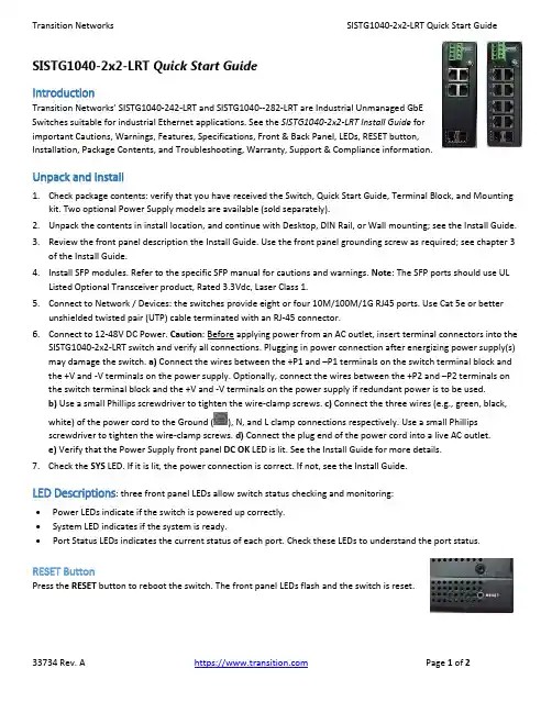
SISTG1040-2x2-LRT Quick Start GuideIntroductionTransition Networks’ SISTG1040-242-LRT and SISTG1040--282-LRT are Industrial Unmanaged GbESwitches suitable for industrial Ethernet applications. See the SISTG1040-2x2-LRT Install Guide forimportant Cautions, Warnings, Features, Specifications, Front & Back Panel, LEDs, RESET button,Installation, Package Contents, and Troubleshooting, Warranty, Support & Compliance information.Unpack and Install1.Check package contents: verify that you have received the Switch, Quick Start Guide, Terminal Block, and Mountingkit. Two optional Power Supply models are available (sold separately).2.Unpack the contents in install location, and continue with Desktop, DIN Rail, or Wall mounting; see the Install Guide.3.Review the front panel description the Install Guide. Use the front panel grounding screw as required; see chapter 3of the Install Guide.4.Install SFP modules. Refer to the specific SFP manual for cautions and warnings. Note: The SFP ports should use ULListed Optional Transceiver product, Rated 3.3Vdc, Laser Class 1.5.Connect to Network / Devices: the switches provide eight or four 10M/100M/1G RJ45 ports. Use Cat 5e or betterunshielded twisted pair (UTP) cable terminated with an RJ-45 connector.6.Connect to 12-48V DC Power. Caution: Before applying power from an AC outlet, insert terminal connectors into theSISTG1040-2x2-LRT switch and verify all connections. Plugging in power connection after energizing power supply(s) may damage the switch. a) Connect the wires between the +P1 and –P1 terminals on the switch terminal block and the +V and -V terminals on the power supply. Optionally, connect the wires between the +P2 and –P2 terminals on the switch terminal block and the +V and -V terminals on the power supply if redundant power is to be used.b) Use a small Phillips screwdriver to tighten the wire-clamp screws. c) Connect the three wires (e.g., green, black,white) of the power cord to the Ground (), N, and L clamp connections respectively. Use a small Phillipsscrewdriver to tighten the wire-clamp screws. d) Connect the plug end of the power cord into a live AC outlet.e) Verify that the Power Supply front panel DC OK LED is lit. See the Install Guide for more details.7.Check the SYS LED. If it is lit, the power connection is correct. If not, see the Install Guide.LED Descriptions: three front panel LEDs allow switch status checking and monitoring:•Power LEDs indicate if the switch is powered up correctly.•System LED indicates if the system is ready.•Port Status LEDs indicates the current status of each port. Check these LEDs to understand the port status.RESET ButtonPress the RESET button to reboot the switch. The front panel LEDs flash and the switch is reset.Front PanelsSISTG1040-242-LRT SISTG1040-282-LRT LED SummaryLED Color FunctionSYS (System) Green On = the switch is ready. Of = the switch is not ready.P1 (Power 1) Green Input Power source 1 supplying power. P2 (Power 2) Green Input Power source 2 supplying power.Link/Act/Speed Green/AmberLight off: port disconnected or link failed.Green Light on: 1G Link Present, No Activity.Amber Light on: 100M/10M Link Present, No Activity.Green Blinking: 1G Activity. Port is sending or receiving data.Amber Blinking: 100M/10M Activity. Port is sending or receiving data.Link/Act/Speed Green/AmberLNK: Amber/Green (Two Color)Light off: port disconnected or link failedAmber Light on: link-up (100M)Green Light on: link-up (1G)Blinking: activity (receiving or transmitting data)Contact UsFor Transition Networks Drivers, Firmware, etc. go to the Product Support webpage (logon required).For Manuals, Application Notes, Brochures, Data Sheets, Specifications, etc. go to the Support Library (no logon required).Transition Networks | 10900 Red Circle Drive | Minnetonka, MN 55343, U.S.A.Technical Support: Technical support is available 24-hours a day. US and Canada: 1-800-260-1312;International: 00-1-952-941-7600. | tel: +1.952.941.7600 | toll free: 1.800.526.9267 | fax: 952.941.2322 ******************** | ************************** | ******************************。
FLIR A6750sc MWIRThermal imaging camera with FLIR cooled InSb detector HIGH SENSITIVITY, CRISP THERMAL IMAGESFLIR A6750sc incorporates a cooled FLIR Indium Antimonide (InSb) detector that operates in the 3- to 5-micron waveband. Optionally, a broadbandversion that operates in the 1-5 micron waveband is available. Both versions produce crisp thermal images of 640 x 512. Achieving a high thermal sensitivity of <20 mK, FLIR A6700sc is able to capture the finest image details.FAST INTEGRATION TIMESWorking in snapshot mode, the FLIR A6750sc is able to capture all pixels from a scene simultaneously in under 190µs for room temperature scenes. This is particularly important when monitoring fast moving objects where an uncooled thermal imaging camera would suffer from image blur. The camera supports image frame rates up to 4.1k frames per second when operating in windowing mode.STANDARD VIDEO INTERFACESUsing a standard GigE Vision ® interface to transmit full dynamic range digital video, and GenICam for camera control, the FLIR A6750sc is a true “plug and play” thermal imaging camera. Additional interfaces include a BNC analog video output. The Gigabit Ethernet and analog video are simultaneously active yet independently controlled allowing greater flexibility for recording and display purposes.CUSTOM COLD FILTERS AVAILABLECustom cold filtering options for specific spectral detection and measurement are available. Perfect for imaging through glass, measuring temperature of thin film plastics, laser profiling and detection, or optical gas imagingSOFTWAREFLIR A6750sc camera works seamlessly with FLIR ResearchIR Max software enabling intuitive viewing, recording and advanced processing of thethermal data provided by the camera. A Software Developers Kit (SDK) is optionally available.COMPATIBLE WITH 3RD PARTY SOFTWARE Control the A6750sc and capture data directly into MathWorks ® MATLAB software for custom image analysis and enhancement.KEY FEATURES• FLIR built cryo cooler and insb detector• Excellent image quality: 640 x 512 pixels • High sensitivity: <20 mK• High speed image acquisition: up to 4,1 kHz in windowing mode• Synchronization with other instruments and events • Wide choice of optics & extender ringsElectronics microscopyMotorcycle brake testingImaging Specifications NASDAQ: FLIRSpecifications are subject to change without notice©Copyright 2015, FLIR Systems, Inc. All other brand and product names are trademarks of their respective owners. The images displayed may not be representative of the actual resolution of the camera shown. Images for illustrative purposes only. (Created 04/15)PORTLANDCorporate Headquarters FLIR Systems, Inc.27700 SW Parkway Ave.Wilsonville, OR 97070USAPH: +1 866.477.3687BELGIUMFLIR Systems Trading Belgium BVBALuxemburgstraat 22321 Meer BelgiumPH: +32 (0) 3665 5100SWEDENFLIR Systems AB Antennvägen 6, PO Box 7376SE-187 66 Täby SwedenPH: +46 (0)8 753 25 00NASHUAFLIR Systems, Inc.9 Townsend West Nashua, NH 06063USAPH: +1 603.324.7611UKFLIR Systems UK 2 Kings Hill Avenue Kings HillWest Malling - Kent ME19 4AQUnited KingdomPH: +44 (0)1732 220 011On/Off switchStatus LEDsPower inCat 6 Ethernet portSyncVideo portAUX port。
Hardware Installation InstructionsTH-1040-RCAComponents ChecklistIMPORTANT INFORMATION! IMPORTANT - Install Telehook 1040 Raked Ceiling Accessory as per Installation Instructions.! This product is to be installed in conjuction with TH-1040-CTS and TH-1040-CTL Ceiling Mounts only.! Supports maximum angle of 45°.! The manufacturer does not accept responsibility for incorrect installation.Step 1. Check ComponentsStep 2. Mount Ceiling Adapter to Ceiling using hardware supplied with TH-1040-CTS/TH-1040-CTL Tools Required:• Power Drill• 7mm (0.25”) drill bit• 12mm (0.5”) masonry drill bit • 17mm (0.69”) Socket Wrench or ShifterCheck you have received all parts against the component checklist and Hardware above.6mm Allen KeyRaked Ceiling Adapter(use hardware fromTH-1040-CTS or TH-1040-CTL)Step 3. Install PoleInstallation Complete, continue with installation of TH-1040-CTS/TH-1040-CTL from Step. 6 onwards.Step 4. Adjust Angle Masonry CeilingTimber CeilingCoach Screw (x4)Raked Ceiling AdapterNylon Anchor (x4)12mm (0.5”)HoleCoach Screw (x4)Raked Ceiling Adapter7mm (0.25”)HoleA. SCREW IN POLEB. INSERTSET SCREWA. LOOSEN SOCKET CAP SCREWB. SET ANGLE OF POLEC. TIGHTEN SOCKET CAP SCREWORSet Screw 3mm Allen KeySet Screw and 3mm Allen Key from TH-1040-CTS or TH-1040-CTL6mm Allen KeySocket Cap ScrewNo portion of this document or any artwork contained herein should be reproduced in any way without the express written consent Atdec Pty Ltd.Due to continuing product development, the manufacturer reserves the right to alter specifications without noticed. Published 07.06.10 ©。
1145HVAAutomotive high voltage fast-acting brick fuseProduct features• Automotive grade qualified*• 11 x 5.0 x 5.0 mm surface mount package • High voltage fast-acting brick fuse• 500 Vdc voltage rating• Ceramic tube, silver plated cap construction • Moisture sensitivity level (MSL): 1*Meets Eaton’s internal AEC-Q200 test plan ApplicationsPrimary and secondary circuit protection:• Stationary and on-board electric vehicle battery systems• Electric vehicle power distribution units (Sensing lines)• xEV powertrains• Server & telecom systems, including 380 Vdc distribution• Single phase and 3-phase UPS• 380 Vdc DC-DC converters• High voltage DC-DC conversion• Power factor correction• Capacitor output protectionAgency informationcURus Recognition file number:E19180, Guide JDYX2Environmental complianceHALOGENHFFREETR- 1145HVA 1-25 -RPackaging codeFamily codeAmpere ratingRoHS compliantOrdering part numberPackaging prefixTR- (1000 parts on a 13” diameter tape and reel)2Technical Data ELX1040Effective May 20211145HVAAutomotive high voltage fast-acting brick fuse/electronicsElectrical characteristicsAmp Rating125% In minimum200% In maximum1000% In maximum1 A ~ 5 A 1 hour 120 seconds 1 secondDimensions- mmDrawing not to scaleRating L W H1 A ~ 5 A 11.2 ± 0.50 2.8 ± 0.50 5.05 ± 0.50Recommended pad layoutRecommended trace thickness is 35 um; the minimum trace width is 5 mmRecommended stencil thickness is 0.15 mm1145HVA is also compatible with Littelfuse LF885 pad layout; pad size 7.23 mm x 5.26 mmProduct specificationsCurrent rating Voltage rating Interrupting rating@ rated voltage 1Typicalresistance 2Typicalvoltage drop Typical pre-arcing 3Part number (A)(Vac)(Vdc)(A) Vac (A) Vdc(mΩ)(mV)I²t (A 2s)Part marking1145HVA1-R 1350500 350100100 A @ 500 Vdc 1500 A @350 Vdc 2002200.5011145HVA1-25-R 1.25350500 350100100 A @ 500 Vdc 1500 A @ 350 Vdc 1602100.95 1.251145HVA1-6-R 1.6350500 350100100 A @ 500 Vdc 1500 A @ 350 Vdc 100190 2.3 1.61145HVA2-R 2350500 350100100 A @ 500 Vdc 1500 A @ 350 Vdc 80185 4.121145HVA2-5-R 2.5350500 350100100 A @ 500 Vdc 1500 A @ 350 Vdc 40120 2.6 2.51145HVA3-15-R 3.15350500 350100100 A @ 500 Vdc 1500 A @ 350 Vdc 31.5140 3.3 3.151145HVA4-R 4350450125100100 A @ 450 Vdc 1500 A @ 125 Vdc 24.5140 5.541145HVA5-R5350450125100100 A @ 450 Vdc 1500 A @ 125 Vdc17.513011.551. AC Interrupting Rating (measured at designated voltage, 100% power factor); DC Interrupting Rating (measured at designated voltage, time constant of less than 50 microseconds, battery source)2.DC Cold Resistance are measured at <10% of rated current in ambient temperature of +25 °C3.Typical Pre-arcing I 2t are measured at 10In Current, DC battery bank3Technical Data ELX1040Effective May 20211145HVAAutomotive high voltage fast-acting brick fuse/electronics Packaging information - mm1000 parts per 13” diameter reel (EIA-481 compliant)DimensionmillimeterW 24.00F 11.50E1 1.75E2N/A P0 4.00P18.00P2 2.00DO 1.50D1 1.50A0 4.85B012.75K0 4.90T0.40Reel dimension- mmDimensionmillimeterA 330 ± 1B 2.5 ± 0.2C 13.5 ± 0.2D N/A N 100 ± 0.5W124.8 ±-0.5W230.4 max W3N/AGeneral specificationsOperating temperature: -55 °C to +125 °C with proper derating factor applied Automotive grade qualified*Temperature cycling: MIL-STD-202 method 107, -55 °C/+125 °C, number of cycles 1000, maximum transfer time 20 seconds, dwell time15 minutes air-air. Humidity bias: MIL-STD-202 method 103, 1000 hours +85 °C/85%RH, 10% of operating powerHigh temperature operating life: MIL-STD-202 method 108, condition D steady state TA=+125 °C at 50% rated current Mechanical shock: MIL-STD-202 method 213, Figure 1 of Method 213, condition C 100 g, 6 msVibration: MIL-STD-202 method 204, 20 g’s for 20 minutes, 12 cycles each of 3 orientations. test from 10-2000 Hz Solderability test: J-STD-002, method B1, steam aging 1 hour, solder temperature +255±5 °C, solder immersion time 5s Board flex: AEC-Q200-005, appendix 2 note: 2 mm (min)Terminal strength (SMD): AEC-Q200-006, appendix 1, force of 1.8 kg for 60 seconds High temperature exposure: MIL-STD-202, method 108, +125 °C without power, 1000 hours ESD: AEC-Q200-002 or ISO/DIS10605, Per AEC-Q200-002 or ISO/DIS10605* Meets Eaton’s internal AEC-Q200 test plan4Technical Data ELX1040Effective May 20211145HVAAutomotive high voltage fast-acting brick fuse/electronicsT emperature derating curveCurrent vs. time curve D e r a t i n g f a c t o rT emperature (°C)Current (A)T i m e (s e c o n d s )Time (seconds)I 2t vs. time curveI 2t (A 2s )EatonElectronics Division 1000 Eaton Boulevard Cleveland, OH 44122United States/electronics© 2021 EatonAll Rights Reserved Printed in USAPublication No. ELX1040 BU-ELX21040May 2021Technical Data ELX1040Effective May 20211145HVAAutomotive high voltage fast-acting brick fuse Life Support Policy: Eaton does not authorize the use of any of its products for use in life support devices or systems without the express writtenapproval of an officer of the Company. Life support systems are devices which support or sustain life, and whose failure to perform, when properly used in accordance with instructions for use provided in the labeling, can be reasonably expected to result in significant injury to the user.Eaton reserves the right, without notice, to change design or construction of any products and to discontinue or limit distribution of any products. Eaton also reserves the right to change or update, without notice, any technical information contained in this bulletin.Solder reflow profileT e m p e r a t u r eT LTPEaton is a registered trademark.All other trademarks are property of their respective owners.Follow us on social media to get the latest product and support information.Reference J-STD-020Profile featureStandard SnPb solderLead (Pb) free solderPreheat and soak • Temperature min. (T smin )100 °C 150 °C • Temperature max. (T smax )150 °C 200 °C • Time (T smin to T smax ) (t s )60-120 seconds 60-120 seconds Ramp up rate T L to T p3 °C/ second max. 3 °C/ second max.Liquidous temperature (T l ) Time (t L ) maintained above T L183 °C60-150 seconds 217 °C60-150 seconds Peak package body temperature (T P )*Table 1Table 2Time (t p )* within 5 °C of the specified classification temperature (T c )20 seconds*30 seconds*Ramp-down rate (T p to T L ) 6 °C/ second max. 6 °C/ second max.Time 25 °C to peak temperature6 minutes max.8 minutes max.* Tolerance for peak profile temperature (T p ) is defined as a supplier minimum and a user maximum.Table 1 - Standard SnPb solder (T c )Package thicknessVolume mm3 <350Volume mm3 ≥350<2.5 mm 235 °C 220 °C ≥2.5 mm220 °C220 °CTable 2 - Lead (Pb) free solder (T c )Package thicknessVolume mm 3 <350Volume mm 3350 - 2000Volume mm 3 >2000<1.6 mm 260 °C 260 °C 260 °C 1.6 – 2.5 mm 260 °C 250 °C 245 °C >2.5 mm250 °C245 °C245 °C。
FEATURES APPLICATIONSDESCRIPTIONVCANHCANLRXDTXDSTBSPLITSN65HVD1040SLLS631B–MARCH2007–REVISED APRIL2007 LOW-POWER CAN TRANSCEIVER WITH BUS WAKE-UP•Battery Operated Applications•Improved Drop-in Replacement for theTJA1040•Hand-Held Diagnostics•Medical Scanning and Imaging•±12kV ESD Protection•HVAC•Low-Current Standby Mode with Bus•Security SystemsWake-up:5µA Typical•Telecom Base Station Status and Control •Bus-Fault Protection of–27V to40V•SAE J1939Standard Data Bus Interface •Rugged Split-Pin Bus Stability•NMEA2000Standard Data Bus Interface •Dominant Time-Out Function•ISO11783Standard Data Bus Interface •Power-Up/Down Glitch-Free Bus Inputs and•Industrial AutomationOutputs–DeviceNet™Data Buses –High Input Impedance with Low V CC–Monotonic Outputs During Power Cycling•DeviceNet Vendor ID#806The SN65HVD1040meets or exceeds the specifications of the ISO11898standard for use in applications employing a Controller Area Network(CAN).As CAN transceivers,these devices provide differential transmit and receive capability for a CAN controller at signaling rates of up to1megabit per second(Mbps).(1) Designed for operation in especially harsh environments,the device features±12kV ESD protection on the bus and split pins,cross-wire,overvoltage and loss of ground protection from–27to40V,overtemperature shutdown,a–12V to12V common-mode range,and will withstand voltage transients from–200V to200V according to ISO7637.(1)The signaling rate of a line is the number of voltage transitions that are made per second expressed in the units bps(bits per second).Please be aware that an important notice concerning availability,standard warranty,and use in critical applications of TexasInstruments semiconductor products and disclaimers thereto appears at the end of this data sheet.DeviceNet is a trademark of Texas Instruments.PRODUCTION DATA information is current as of publication date.Copyright©2007,Texas Instruments Incorporated Products conform to specifications per the terms of the TexasInstruments standard warranty.Production processing does notnecessarily include testing of all parameters.V SN65HVD1040SN65HVD1040SLLS631B–MARCH 2007–REVISED APRIL 2007These devices have limited built-in ESD protection.The leads should be shorted together or the device placed in conductive foam during storage or handling to prevent electrostatic damage to the MOS gates.The STB input (pin 8)selects between two different modes of operation;high-speed or low-power mode.The high-speed mode of operation is selected by connecting STB to ground.If a high logic level is applied to the STB pin of the SN65HVD1040,the device enters a low-power bus-monitor standby mode.While the SN65HVD1040is in the low-power bus-monitor standby mode,a dominant bit greater than 5µs on the bus is passed by the bus-monitor circuit to the receiver output.The local protocol controller may then reactivate the device when it needs to transmit to the bus.A dominant-time-out circuit in the SN65HVD1040prevents the driver from blocking network communication during a hardware or software failure.The time-out circuit is triggered by a falling edge on TXD (pin 1).If no rising edge is seen before the time-out constant of the circuit expires,the driver is disabled.The circuit is then reset by the next rising edge on TXD.The SPLIT output (pin 5)is available on the SN65HVD1040as a V CC /2common-mode bus voltage bias for a split-termination network.The SN65HVD1040is characterized for operation from –40°C to 125°C.ORDERING INFORMATIONDOMINANT LOW-POWER MARKED PART NUMBER PACKAGE (1)ORDERING NUMBER TIME-OUTBUS MONITORAS SN65HVD1040D (rail)SN65HVD1040YESYESSOIC-8VP1040SN65HVD1040DR (reel)(1)For the most current package and ordering information,see the Package Option Addendum at the end of this document,or see the TI website at .2Submit Documentation FeedbackABSOLUTE MAXIMUM RATINGS(1) RECOMMENDED OPERATING CONDITIONSSUPPLY CURRRENTDEVICE SWITCHING CHARACTERISTICSSN65HVD1040 SLLS631B–MARCH2007–REVISED APRIL2007VALUEV CC Supply voltage(2)–0.3V to7VV I(bus)Voltage range at any bus terminal(CANH,CANL,SPLIT)–27V to40VI O(OUT)Receiver output current-20mA to20mAVoltage input,transient pulse(3),(CANH,CANL,SPLIT)–200V to200VHuman Body Model Bus terminals and GND±12kVHuman body model(4)All pins±4kVESDCharged-device-model(5)All pins±1kVMachine model±200VV I Voltage input range(TXD,STB)–0.5V to6VT J Junction temperature–55°C to170°C(1)Stresses beyond those listed under"absolute maximum ratings"may cause permanent damage to the device.These are stress ratingsonly and functional operation of the device at these or any other conditions beyond those indicated under"recommended operating conditions"is not implied.Exposure to absolute-maximum-rated conditions for extended periods may affect device reliability.(2)All voltage values,except differential I/O bus voltages,are with respect to network ground terminal.(3)Tested in accordance with ISO7637,test pulses1,2,3a,3b,5,6&7.(4)Tested in accordance JEDEC Standard22,Test Method A114-A.(5)Tested in accordance JEDEC Standard22,Test Method C101.MIN NOM MAX UNITV CC Supply voltage 4.75 5.25VV I or V IC Voltage at any bus terminal(separately or common mode)–12(1)12VV IH High-level input voltage2 5.25VTXD,STBV IL Low-level input voltage00.8VV ID Differential input voltage–66VDriver–70I OH High-level output current mAReceiver–2Driver70I OL Low-level output current mAReceiver2t SS Maximum pulse width to remain in standby0.7µsT J Junction temperature–40150 C (1)The algebraic convention,in which the least positive(most negative)limit is designated as minimum is used in this data sheet.over operating free-air temperature range(unless otherwise noted)PARAMETER TEST CONDITIONS MIN TYP MAX UNITDominant V I=0V,60ΩLoad,STB at0V5070mAI CC Supply current,V CC Recessive V I=V CC,STB at0V610Standby STB at VCC,VI=VCC512µAover recommended operating conditiions(unless otherwise noted)TEST MIN TYP MAX UNITPARAMETERCONDITIONSt loop1Total loop delay,driver input to receiver output,Recessive to Dominant90230STB at0V,nsSee Figure9t loop2Total loop delay,driver input to receiver output,Dominant to Recessive902303Submit Documentation FeedbackDRIVER ELECTRICAL CHARACTERISTICSDRIVER SWITCHING CHARACTERISTICSSN65HVD1040SLLS631B–MARCH 2007–REVISED APRIL 2007over recommended operating conditiions (unless otherwise noted)PARAMETERTEST CONDITIONSMIN TYP (1)MAX UNIT CANH 2.9 3.44.5Bus output voltage V I =0V,STB at 0V,R L =60Ω,See Figure 1and V O(D)V (Dominant)Figure 2CANL0.8 1.75V O(R)Bus output voltage (Recessive)V I =3V,STB at 0V,See Figure 1and Figure 22 2.53V V O Bus output voltage (Standby)R L =60Ω,STB at V CC ,See Figure 1and Figure 2–0.10.1VV I =0V,R L =60Ω,STB at 0V,See Figure 1and 1.53Figure 2,and Figure 3V OD(D)Differential output voltage (Dominant)V V I =0V,R L =45Ω,STB at 0V,See Figure 1and 1.43Figure 2Output symmetry (Dominant or V SYM STB at 0V,See Figure 2and Figure 130.9×V CC V CC 1.1×V CCV Recessive)[V O(CANH)+V O(CANL))V I =3V,R L =60Ω,STB at 0V,See Figure 1and–0.0120.012Figure 2V OD(R)Differential output voltage (Recessive)VV I =3V,STB at 0V,No Load –0.50.05Common-mode output voltage V OC(D)22.33(Dominant)STB at 0V,See Figure 8V Peak-to-peak common-mode output V OC(pp)0.3voltageI IH High-level input current,TXD input V I at V CC –22µA I IL Low-level input current,TXD input V I at 0V–50–10µA I O(off)Power-off TXD Leakage currentV CC at 0V,TXD at 5V1µAV CANH =–12V,CANL Open,See Figure 12–120–72V CANH =12V,CANL Open,See Figure 120.361Short-circuit steady-state output I OS(ss)mAcurrentV CANL =–12V,CANH Open,See Figure 12–1–0.5V CANL =12V,CANH Open,See Figure 1271120See Input capacitance to ground in RECEIVER C O Output capacitanceELECTRICAL CHARACTERISTICS .(1)All typical values are at 25 C with a 5-V supply.over recommended operating conditions (unless otherwise noted)PARAMETERTEST CONDITIONSMIN TYP MAX UNITt PLH Propagation delay time,low-to-high-level output 2565120t PHL Propagation delay time,high-to-low-level output 2545120t sk(p)Pulse skew (|t PHL –t PLH |)STB at 0V,See Figure 425ns t r Differential output signal rise time 25t f Differential output signal fall time50t en Enable time from silent mode to dominant See Figure 710µs t domDominant time-outSee Figure 10300450700µs4Submit Documentation FeedbackRECEIVER ELECTRICAL CHARACTERISTICS RECEIVER SWITCHING CHARACTERISTICSSPLIT-PIN CHARACTERISTICSSTB-PIN CHARACTERISTICSSN65HVD1040 SLLS631B–MARCH2007–REVISED APRIL2007over recommended operating conditions(unless otherwise noted)PARAMETER TEST CONDITIONS MIN TYP(1)MAX UNITPositive-going input thresholdV IT+800900 voltageSTB at0V,See Table1High-speedNegative-going input thresholdV IT–mode500650mV voltageV hys Hysteresis voltage(V IT+–V IT–)STB at V CC100125V IT Input threshold voltage Standby mode STB at V CC5001150V OH High-level output voltage I O=–2mA,See Figure64 4.6VV OL Low-level output voltage I O=2mA,See Figure60.20.4VCANH or CANL=5V,V CC at0V,I I(off)Power-off bus input current5µATXD at0VI O(off)Power-off RXD leakage current V CC at0V,RXD at5V20µAC I Input capacitance to ground,(CANH or CANL)TXD at3V,V I=0.4sin(4E6πt)+2.5V20pFC ID Differential input capacitance TXD at3V,V I=0.4sin(4E6πt)10pFR ID Differential input resistance TXD at3V,STD at0V3080kΩR IN Input resistance,(CANH or CANL)TXD at3V,STD at0V153040Input resistance matchingR I(m)V CANH=V CANL–3%0%3% [1–(R IN(CANH)/R IN(CANL))]x100%(1)All typical values are at25 C with a5-V supply.over recommended operating conditiions(unless otherwise noted)PARAMETER TEST CONDITIONS MIN TYP MAX UNITt pLH Propagation delay time,low-to-high-level output60100130t pHL Propagation delay time,high-to-low-level output4570130STB at0V,TXD at3V,SeensFigure6t r Output signal rise time8t f Output signal fall time8t BUS Dominant time required on bus for wake-up fromSTB at V CC Figure110.75µs standby(1)(1)The device under test shall not signal a wake-up condition with dominant pulses shorter than t BUS(min)and shall signal a wake-upcondition with dominant pulses longer than t BUS(max).Dominant pulses with a length between t BUS(min)and t BUS(max)may lead to a wake-up.over recommended operating conditiions(unless otherwise noted)PARAMETER TEST CONDITIONS MIN TYP MAX UNITV O Output voltage–500µA<I O<500µA0.3×V CC0.5×V CC0.7×V CC VI O(stb)Standby mode leakage current STB at2V,–12V≤V O≤12V–55µAover recommended operating conditiions(unless otherwise noted)PARAMETER TEST CONDITIONS MIN TYP MAX UNIT I IH High level input current STB at2V–100µAI IL Low level input current STB at0V–100µA5Submit Documentation FeedbackPARAMETER MEASUREMENT INFORMATION2.5 V3.5 V 1.5 VRecessiveDominantO (CANH)V O (CANL)VI−2 V 3 V TEST 3 7 VV O(D)O(R)+20%V CC V I V I I OV I(CANH) + V I(CANL)2V IC =SN65HVD1040SLLS631B–MARCH 2007–REVISED APRIL 2007Figure 1.Driver Voltage,Current,and Test DefinitionFigure 2.Bus Logic State Voltage DefinitionsFigure 3.Driver V OD Test CircuitFigure 4.Driver Test Circuit and Voltage WaveformsFigure 5.Receiver Voltage and Current Definitions6Submit Documentation FeedbackOOHVOLC L= 15 pF20%(see Note B)CC60 W+1%V CC0 VV OHV OLV ISN65HVD1040SLLS631B–MARCH2007–REVISED APRIL2007 PARAMETER MEASUREMENT INFORMATION(continued)A.The input pulse is supplied by a generator having the following characteristics:PRR≤125kHz,50%duty cycle,t r≤6ns,t f≤6ns,Z O=50Ω.B.C L includes instrumentation and fixture capacitance within 20%.Figure6.Receiver Test Circuit and Voltage WaveformsTable1.Differential Input Voltage Threshold TestINPUT OUTPUTV CANH V CANL|V ID|R–11.1V–12V900mV L V OL12V11.1V900mV L–6V–12V6V L12V6V6V L–11.5V–12V500mV H V OH12V11.5V500mV H–12V–6V6V H6V12V6V HOpen Open X HFigure7.t en Test Circuit and Voltage WaveformsA.All V I input pulses are from0V to V CC and supplied by a generator having the following characteristics:t r or t f≤6ns.Pulse Repetition Rate(PRR)=125kHz,50%duty cycle.Figure8.Peak-to-Peak Common Mode Output Voltage Test and Waveform7Submit Documentation Feedback60 W +1%V CC0 VV OHVOL V IV OV CC0 V OD(D)OV V OHOL0.7m SN65HVD1040SLLS631B–MARCH 2007–REVISED APRIL 2007A.All V I input pulses are from 0V to V CC and supplied by a generator with the following characteristics:t r or t f ≤6ns.Pulse Repetition Rate (PRR)=125kHz,50%duty cycle.Figure 9.t loop Test Circuit and Voltage WaveformsA.All V I input pulses are from 0V to V CC and supplied by a generator with the following characteristics:t r or t f ≤6ns.Pulse Repetition Rate (PRR)=500Hz,50%duty cycle.B.C L =100pF includes instrumentation and fixture capacitance within 20%.Figure 10.Dominant Time-Out Test Circuit and WaveformA.For V I bit width ≤0.7µs,V O =V OH .For V I I bit width ≥5µs,V O =V OL .V I input pulses are supplied from a generator with the following characteristics;t r or t f ≤6ns.Pulse Repetition Rate (PRR)=50Hz,30%duty cycle.B.C L =15pF includes instrumentation and fixture capacitance within 20%.Figure 11.t BUS Test Circuit and Waveform8Submit Documentation Feedback0 V or V V ISYM =+O(CANL)V O (CANH)V SN65HVD1040SLLS631B–MARCH 2007–REVISED APRIL 2007Figure 12.Driver Short-Circuit Current Test and WaveformFigure 13.Driver Output Symmetry Test Circuit9Submit Documentation FeedbackDEVICE INFORMATIONTHERMAL CHARACTERISTICSSN65HVD1040SLLS631B–MARCH 2007–REVISED APRIL 2007Table 2.DRIVER FUNCTION TABLE (1)INPUTS OUTPUTS BUS STATETXD STB CANHCANL L L H L DOMINANT H L Z Z RECESSIVE Open X Z Z RECESSIVE X H or OpenZZRECESSIVE (1)H =high level;L =low level;X =irrelevant;Z =high impedanceTable 3.RECEIVER FUNCTION TABLE (1)DIFFERENTIAL INPUTS STB OUTPUT BUS STATE V ID =CANH -CANLRXDV ID ≥0.9V L L DOMINANT V ID ≥ 1.15V H or OpenL DOMINANT0.5V <V ID <0.9VX ??V ID ≤0.5V X H RECESSIVE OpenXHRECESSIVE(1)H =high level;L =low level;X =irrelevant;?=indeterminate;Z =high impedanceover operating free-air temperature range (unless otherwise noted)PARAMETERTEST CONDITIONSMIN TYP MAX UNIT Low-K Thermal Resistance (1)211°C/W θJA Thermal Resistance,Junction-to-Air High-K Thermal Resistance131°C/WθJB Thermal Resistance,53Junction-to-Board °C/WθJC Thermal Resistance,79Junction-to-Case R L =60Ω,S at 0V,P D Device Power Dissipation112170mW Input to TXD a 500kHz 50%duty-cycle square waveT JS Junction Temperature,Thermal Shutdown(2)190°C(1)Tested in accordance with the Low-K or High-K thermal metric definitions of EIA/JESD51-3for leaded surface mount packages.(2)Extended operation in thermal shutdown may affect device reliability,see the Application Information section.10Submit Documentation FeedbackDEVICE INFORMATIONSN65HVD1040 SLLS631B–MARCH2007–REVISED APRIL2007Table4.Parametric Cross Reference With the TJA1040 TJA1040(1)PARAMETER HVD10xxTJA1040DRIVER SECTIONV IH High-level input voltage Recommended V IHV IL Low-level input voltage Recommended V ILI IH High-level input current Driver I IHI IL Low-level input current Driver I ILTJA1040BUS SECTIONV th(dif)Differential input voltage Receiver V IT and recommended V ID V hys(dif)Differential input hysteresis Receiver V hysV O(dom)Dominant output voltage Driver V O(D)V O(reces)Recessive output voltage Driver V O(R)V i(dif)(th)Differential input voltage Receiver V IT and recommended V ID V O(dif0(bus)Differential bus voltage Driver V OD(D)and V OD(R)I LI Power-off bus input current Receiver I I(off)I O(SC)Short-circuit output current Driver I OS(SS)R i(cm)CANH,CANL input resistance Receiver R INR i(def)Differential input resistance Receiver R IDR i(cm)(m)Input resistance matching Receiver R I(m)C i(cm)Input capacitance to ground Receiver C IC i(dif)Differential input capacitance Receiver C IDTJA1040RECEIVER SECTIONI OH High-level output current Recommended I OHI OL Low-level output current Recommended I OLTJA1040SPLIT PIN SECTIONV O Reference output voltage V OTJA1040TIMING SECTIONt d(TXD-BUSon)Delay TXD to bus active Driver t PLHt d(TXD-BUSoff)Delay TXD to bus inactive Driver t PHLt d(BUSon-RXD)Delay bus active to RXD Receiver t PHLt d(BUSoff-RXD)Delay bus inactive to RXD Receiver t PLHt PD(TXD–RXD)Prop delay TXD to RXD Device t LOOP1and t LOOP2t d(stb-norm)Enable time from standby to dominant Driver t enTJA1040STB PIN SECTIONV IH High-level input voltage Recommended V IHV IL Low-level input voltage Recommended V ILI IH High-level input current I IHI IL Low-level input current I IL(1)From TJA1040Product Specification,Philips Semiconductors,2003February19.Equivalent Input and Output Schematic DiagramsSN65HVD1040SLLS631B–MARCH 2007–REVISED APRIL 2007TYPICAL CHARACTERISTICS−4002570125−R e c e s s i v e -t o -D o m i n a n t L o o p Ti m e −n s t L O O P 1T A −Free-Air T emperature −°C−4002570125−D o m i n a n t -t o -R e c e s s i v e L o o p Ti m e −n s t L O O P 2T A −Free-Air T emperature −°C−100102030405060708090012345I O L − L o w -L e v e l O u t p u t C ur r e n t − m AV O CANL − Low-Level Output Voltage − V5101520253035404550Signaling Rate − kbpsI C C − R M S S u p p l y C u r r e n t − m ASN65HVD1040SLLS631B–MARCH 2007–REVISED APRIL 2007RECESSIVE-TO-DOMINANT LOOP TIMEDOMINANT-TO-RECESSIVE LOOP TIMEvsvsFREE-AIR TEMPERATURE (across V CC )FREE-AIR TEMPERATURE (across V CC )Figure 14.Figure 15.SUPPLY CURRENT (RMS)DRIVER LOW-LEVEL OUTPUT VOLTAGEvsvsSIGNALING RATELOW-LEVEL OUTPUT CURRENTFigure 16.Figure 17.-0-10-20-30-40-50-60-70-80012345I O H −H i g h -L e v e l O u t p u t C u r r e n t −m AV O CANH −High-Level Output V oltage −V0.511.522.53−4002570125T A − Free-Air Temperature − °CD o m i n a n t D r i v e r D i f f e r e n t i a l O u t p u t V o l t a g e −VI O − D i f f e r e n t i a l D r i v e r O u t p u t C u r r e n t − m AV CC − Supply Voltage − V0.60.60.70.70.80.80.80.80.70.70.60.6− R e c e i v e r O u t p u t V o l t a g e − VV O V ID − Differential Input Voltage − VSN65HVD1040SLLS631B–MARCH 2007–REVISED APRIL 2007TYPICAL CHARACTERISTICS (continued)DRIVER HIGH-LEVEL OUTPUT VOLTAGEDRIVER DIFFERENTIAL OUTPUT VOLTAGEvsvsHIGH-LEVEL OUTPUT CURRENTFREE-AIR TEMPERATURE (across V CC )Figure 18.Figure 19.DRIVER OUTPUT CURRENTRECEIVER OUTPUT VOLTAGEvsvsSUPPLY VOLTAGEDIFFERENTIAL INPUT VOLTAGEFigure 20.Figure 21.D B Vm 0204060800.11101001000f − Frequency − MHzd B mSN65HVD1040SLLS631B–MARCH 2007–REVISED APRIL 2007TYPICAL CHARACTERISTICS (continued)TYPICAL ELECTROMAGNETIC EMISSIONSTYPICAL ELECTROMAGNETIC UP TO 50MHZ (Peak Amplitude)IMMUNITY PERFORMANCEFigure 22.Frequency Spectrum of Common-ModeFigure 23.Direct Power Injection (DPI)Response vsEmissions FrequencyAPPLICATION INFORMATIONCAN BasicsSN65HVD1040SLLS631B–MARCH 2007–REVISED APRIL 2007The basics of arbitration require that the receiver at the sending node designate the first bit as dominant or recessive after the initial wave of the first bit of a message travels to the most remote node on a network and back again.Typically,this “sample”is made at 75%of the bit width,and within this limitation,the maximum allowable signal distortion in a CAN network is determined by network electrical parameters.Factors to be considered in network design include the approximately 5ns/m propagation delay of typical twisted-pair bus cable;signal amplitude loss due to the loss mechanisms of the cable;and the number,length,and spacing of drop-lines (stubs)on a network.Under strict analysis,variations among the different oscillators in a system also need to be accounted for with adjustments in signaling rate and stub and bus length.Table 5lists the maximum signaling rates achieved with the SN65HVD1040with several bus lengths of category 5,shielded twisted pair (CAT 5STP)cable.Table 5.Maximum Signaling Rates for Various CableLengthsBus Length (m)Signaling Rate (kbps)301000100500250250500125100062.5The ISO 11898Standard specifies a maximum bus length of 40m and maximum stub length of 0.3m with a maximum of 30nodes.However,with careful design,users can have longer cables,longer stub lengths,and many more nodes to a bus.(Note:Non-standard application may come with a trade-off in signaling rate.)A large number of nodes requires a transceiver with high input impedance such as the HVD1040.The Standard specifies the interconnect to be a single twisted-pair cable (shielded or unshielded)with 120Ωcharacteristic impedance (Z O ).Resistors equal to the characteristic impedance of the line terminate both ends of the cable to prevent signal reflections.Unterminated drop-lines connect nodes to the bus and should be kept as short as possible to minimize signal reflections.Connectors,while not specified by the standard should have as little effect as possible on standard operating parameters such as capacitive loading.Although unshielded cable is used in many applications,data transmission circuits employing CAN transceivers are usually used in applications requiring a rugged interconnection with a wide common-mode voltage range.Therefore,shielded cable is recommended in these electronically harsh environments,and when coupled with the Standard’s –2-V to 7-V common-mode range of tolerable ground noise,helps to ensure data integrity.The HVD1040enhances the Standard’s insurance of data integrity with an extended –12V to 12V range of common-mode operation.500mV ThresholdmV ThresholdALLOWABLE JITTERNOISE MARGINW120Wm FSN65HVD1040SLLS631B–MARCH 2007–REVISED APRIL 2007Figure 24.Typical CAN Differential Signal Eye-PatternAn eye pattern is a useful tool for measuring overall signal quality.As displayed in Figure 25,the differential signal changes logic states in two places on the display,producing an “eye.”Instead of viewing only one logic crossing on the scope,an entire “bit”of data is brought into view.The resulting eye pattern includes all of the effects of systemic and random distortion,and displays the time during which a signal may be considered valid.The height of the eye above or below the receiver threshold voltage level at the sampling point is the noise margin of the system.Jitter is typically measured at the differential voltage zero-crossing during the logic state transition of a signal.Note that jitter present at the receiver threshold voltage level is considered by some to be a more effective representation of the jitter at the input of a receiver.As the sum of skew and noise increases,the eye closes and data is corrupted.Closing the width decreases the time available for accurate sampling,and lowering the height enters the 900mV or 500mV threshold of a receiver.Different sources induce noise onto a signal.The more obvious noise sources are the components of a transmission circuit themselves;the signal transmitter,traces and cables,connectors,and the receiver.Beyond that,there is a termination dependency,cross-talk from clock traces and other proximity effects,V CC and ground bounce,and electromagnetic interference from near-by electrical equipment.The balanced receiver inputs of the HVD1040mitigate most all sources of signal corruption,and when used with a quality shielded twisted-pair cable,help insure data integrity.Figure 25.Typical HVD1040ApplicationThermal ShutdownSN65HVD1040SLLS631B–MARCH 2007–REVISED APRIL 2007The SN65HVD1040has a thermal shutdown that turns off the driver outputs when the junction temperature nears 190°C.This shutdown prevents catastrophic failure from bus shorts,but does not protect the circuit from possible damage.The user should strive to maintain recommended operating conditions,and not exceed absolute maximum ratings at all times.If the SN65HVD1040is subjected to many or long durations faults that can put the device into thermal shutdown,it should be replaced.PACKAGING INFORMATIONOrderable Device Status (1)Package Type Package DrawingPins Package Qty Eco Plan (2)Lead/Ball Finish MSL Peak Temp (3)SN65HVD1040D ACTIVE SOIC D 875Green (RoHS &no Sb/Br)CU NIPDAU Level-1-260C-UNLIM SN65HVD1040DG4ACTIVE SOIC D 875Green (RoHS &no Sb/Br)CU NIPDAU Level-1-260C-UNLIM SN65HVD1040DR ACTIVE SOIC D 82500Green (RoHS &no Sb/Br)CU NIPDAU Level-1-260C-UNLIM SN65HVD1040DRG4ACTIVESOICD82500Green (RoHS &no Sb/Br)CU NIPDAULevel-1-260C-UNLIM(1)The marketing status values are defined as follows:ACTIVE:Product device recommended for new designs.LIFEBUY:TI has announced that the device will be discontinued,and a lifetime-buy period is in effect.NRND:Not recommended for new designs.Device is in production to support existing customers,but TI does not recommend using this part in a new design.PREVIEW:Device has been announced but is not in production.Samples may or may not be available.OBSOLETE:TI has discontinued the production of the device.(2)Eco Plan -The planned eco-friendly classification:Pb-Free (RoHS),Pb-Free (RoHS Exempt),or Green (RoHS &no Sb/Br)-please check /productcontent for the latest availability information and additional product content details.TBD:The Pb-Free/Green conversion plan has not been defined.Pb-Free (RoHS):TI's terms "Lead-Free"or "Pb-Free"mean semiconductor products that are compatible with the current RoHS requirements for all 6substances,including the requirement that lead not exceed 0.1%by weight in homogeneous materials.Where designed to be soldered at high temperatures,TI Pb-Free products are suitable for use in specified lead-free processes.Pb-Free (RoHS Exempt):This component has a RoHS exemption for either 1)lead-based flip-chip solder bumps used between the die and package,or 2)lead-based die adhesive used between the die and leadframe.The component is otherwise considered Pb-Free (RoHS compatible)as defined above.Green (RoHS &no Sb/Br):TI defines "Green"to mean Pb-Free (RoHS compatible),and free of Bromine (Br)and Antimony (Sb)based flame retardants (Br or Sb do not exceed 0.1%by weight in homogeneous material)(3)MSL,Peak Temp.--The Moisture Sensitivity Level rating according to the JEDEC industry standard classifications,and peak solder temperature.Important Information and Disclaimer:The information provided on this page represents TI's knowledge and belief as of the date that it is provided.TI bases its knowledge andbelief on information provided by third parties,and makes no representation or warranty as to the accuracy of such information.Efforts are underway to better integrate information from third parties.TI has taken and continues to take reasonable steps to provide representative and accurate information but may not have conducted destructive testing or chemical analysis on incoming materials and chemicals.TI and TI suppliers consider certain information to be proprietary,and thus CAS numbers and other limited information may not be available for release.In no event shall TI's liability arising out of such information exceed the total purchase price of the TI part(s)at issue in this document sold by TI to Customer on an annual basis.PACKAGE OPTION ADDENDUM7-May-2007。