
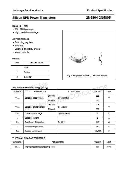
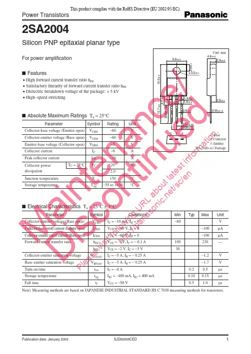
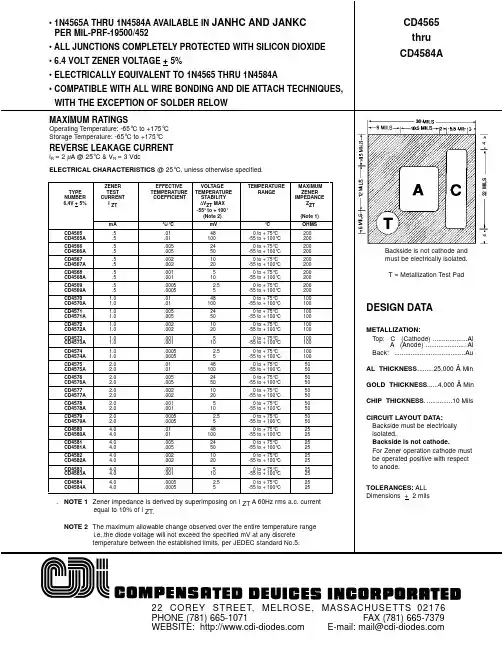
2N5804中文资料
- 格式:pdf
- 大小:119.45 KB
- 文档页数:3
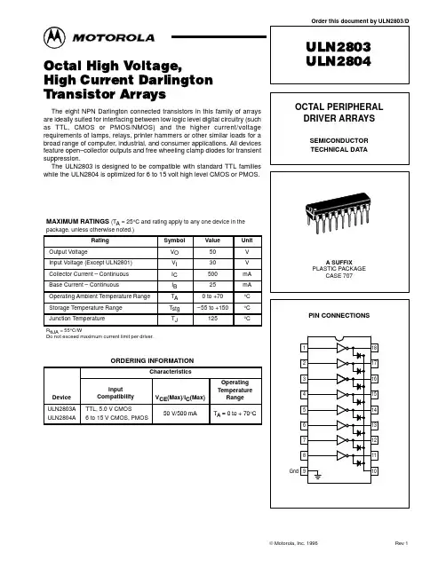

TL F 64945404 DM5404 DM7404 Hex Inverting GatesJune1989 5404 DM5404 DM7404Hex Inverting GatesGeneral DescriptionThis device contains six independent gates each of whichperforms the logic INVERT functionFeaturesY Alternate Military Aerospace device(5404)is availableContact a National Semiconductor Sales Office Distrib-utor for specificationsConnection DiagramDual-In-Line PackageTL F 6494–1Order Number5404DMQB 5404FMQB DM5404J DM5404W DM7404M or DM7404NSee NS Package Number J14A M14A N14A or W14BFunction TableY e AInputs OutputA YL HH LH e High Logic LevelL e Low Logic LevelC1995National Semiconductor Corporation RRD-B30M105 Printed in U S AAbsolute Maximum Ratings(Note)If Military Aerospace specified devices are required please contact the National Semiconductor Sales Office Distributors for availability and specifications Supply Voltage7V Input Voltage5 5V Operating Free Air Temperature RangeDM54and54b55 C to a125 C DM740 C to a70 C Storage Temperature Range b65 C to a150 C Note The‘‘Absolute Maximum Ratings’’are those values beyond which the safety of the device cannot be guaran-teed The device should not be operated at these limits The parametric values defined in the‘‘Electrical Characteristics’’table are not guaranteed at the absolute maximum ratings The‘‘Recommended Operating Conditions’’table will define the conditions for actual device operationRecommended Operating ConditionsSymbol ParameterDM5404DM7404Units Min Nom Max Min Nom MaxV CC Supply Voltage4 555 54 7555 25V V IH High Level Input Voltage22V V IL Low Level Input Voltage0 80 8V I OH High Level Output Current b0 4b0 4mA I OL Low Level Output Current1616mA T A Free Air Operating Temperature b55125070 C Electrical Characteristicsover recommended operating free air temperature range(unless otherwise noted)Symbol Parameter Conditions MinTypMax Units (Note1)V I Input Clamp Voltage V CC e Min I I e b12mA b1 5VV OH High Level Output V CC e Min I OH e Max2 43 4VVoltage V IL e MaxV OL Low Level Output V CC e Min I OL e Max0 20 4VVoltage V IH e MinI I Input Current Max V CC e Max V I e5 5V1mA Input VoltageI IH High Level Input Current V CC e Max V I e2 4V40m AI IL Low Level Input Current V CC e Max V I e0 4V b1 6mAI OS Short Circuit V CC e Max DM54b20b55mA Output Current(Note2)DM74b18b55I CCH Supply Current with V CC e Max612mA Outputs HighI CCL Supply Current with V CC e Max1833mA Outputs LowSwitching Characteristics at V CC e5V and T A e25 C(See Section1for Test Waveforms and Output Load) Symbol Parameter Conditions Min Max Unitst PLH Propagation Delay Time C L e15pF22ns Low to High Level Output R L e400Xt PHL Propagation Delay Time15ns High to Low Level OutputNote1 All typicals are at V CC e5V T A e25 CNote2 Not more than one output should be shorted at a time23Physical Dimensions inches(millimeters)14-Lead Ceramic Dual-In-Line Package(J)Order Number5404DMQB or DM5404JNS Package Number J14A4Physical Dimensions inches(millimeters)(Continued)14-Lead Small Outline Molded Package(M)Order Number DM7404MNS Package Number M14A14-Lead Molded Dual-In-Line Package(N)Order Number DM7404NNS Package Number N14A55404 D M 5404 D M 7404H e x I n v e r t i n g G a t e sPhysical Dimensions inches (millimeters)(Continued)14-Lead Ceramic Flat Package (W)Order Number 5404FMQB or DM5404WNS Package Number W14BLIFE SUPPORT POLICYNATIONAL’S PRODUCTS ARE NOT AUTHORIZED FOR USE AS CRITICAL COMPONENTS IN LIFE SUPPORT DEVICES OR SYSTEMS WITHOUT THE EXPRESS WRITTEN APPROVAL OF THE PRESIDENT OF NATIONAL SEMICONDUCTOR CORPORATION As used herein 1 Life support devices or systems are devices or 2 A critical component is any component of a life systems which (a)are intended for surgical implant support device or system whose failure to perform can into the body or (b)support or sustain life and whose be reasonably expected to cause the failure of the life failure to perform when properly used in accordance support device or system or to affect its safety or with instructions for use provided in the labeling can effectivenessbe reasonably expected to result in a significant injury to the userNational Semiconductor National Semiconductor National Semiconductor National Semiconductor CorporationEuropeHong Kong LtdJapan Ltd1111West Bardin RoadFax (a 49)0-180-530858613th Floor Straight Block Tel 81-043-299-2309。