
silvaco mosfet工艺流程仿真
- 格式:ppt
- 大小:21.24 MB
- 文档页数:108

4.1.7栅氧厚度的最优化下面介绍如何使用DECKBUILD中的最优化函数来对栅极氧化厚度进行最优化。
假定所测量的栅氧厚度为100Å,栅极氧化过程中的扩散温度和偏压均需要进行调整。
为了对参数进行最优化,DECKBUILD最优化函数应按如下方法使用:a.依次点击Main control和Optimizer…选项;调用出如图4.15所示的最优化工具。
第一个最优化视窗显示了Setup模式下控制参数的表格。
我们只改变最大误差参数以便能精确地调整栅极氧化厚度为100Å;b.将Maximum Error在criteria一栏中的值从5改为1;c.接下来,我们通过Mode键将Setup模式改为Parameter模式,并定义需要优化参数(图4.16)。
图4.15 DECKBUILD最优化的Setup模式图4.16 Parameter模式需要优化的参数是栅极氧化过程中的温度和偏压。
为了在最优化工具中对其进行最优化,如图4.17所示,在DECKBUILD窗口中选中栅极氧化这一步骤;图4.17 选择栅极氧化步骤d.然后,在Optimizer中,依次点击Edit和Add菜单项。
一个名为Deckbuild:Parameter Define的窗口将会弹出,如图4.18所示,列出了所有可能作为参数的项;图4.18 定义需要优化的参数e.选中temp=<variable>和press=<variable>这两项。
然后,点击Apply。
添加的最优化参数将如图4.19所示一样列出;图4.19 增加的最优化参数f.接下来,通过Mode键将Parameter模式改为Targets模式,并定义优化目标;g.Optimizer利用DECKBUILD中Extract语句的值来定义优化目标。
因此,返回DECKBUILD的文本窗口并选中Extract栅极氧化厚度语句,如图4.20所示;图4.20 选中优化目标h.然后,在Optimizer中,依次点击Edit和Add项。

9SilvacoTCAD器件仿真模块及器件仿真流程Silvaco TCAD是一种广泛使用的集成电路(IC)设计和仿真工具,用于开发和研究半导体器件。
它提供了一套完整的器件仿真模块,可以帮助工程师设计、优化和验证各种半导体器件的性能。
本文将介绍几个常用的Silvaco TCAD器件仿真模块,并提供一个简要的器件仿真流程。
1. ATHENA模块:ATHENA是Silvaco TCAD的物理模型模拟引擎,用于模拟器件的结构和物理特性。
它可以通过解决泊松方程、电流连续性方程和能带方程等来计算电子和空穴的分布、电场和电势等物理量。
ATHENA支持多种材料模型和边界条件,可以准确地模拟各种器件结构。
2. ATLAS模块:ATLAS是Silvaco TCAD的设备模拟引擎,用于模拟半导体器件的电学和光学特性。
它可以模拟器件的电流-电压特性、载流子分布、能量带结构和光电特性等。
ATLAS支持各种器件类型,如二极管、MOSFET、BJT和太阳能电池等。
3. UTILITY模块:UTILITY是Silvaco TCAD的实用工具模块,用于处理和分析仿真结果。
它提供了各种数据可视化、数据处理和数据导出功能,帮助工程师分析和优化器件性能。
UTILITY还可以用于参数提取和模型校准,以改进模拟的准确性。
接下来是一个简要的Silvaco TCAD器件仿真流程:2. 设置模拟参数:在进行仿真之前,需要设置模拟所需的参数,如材料参数、边界条件、物理模型和仿真选项等。
可以使用Silvaco TCAD的参数设置工具来设置这些参数。
3. 运行ATHENA模拟:使用ATHENA模块进行结构模拟,通过求解泊松方程和连续性方程,计算出电子和空穴的分布、电场和电势等物理量。
可以使用Silvaco TCAD的命令行界面或图形用户界面来运行ATHENA模拟。
4. 运行ATLAS模拟:使用ATLAS模块进行设备模拟,模拟器件的电学和光学特性。
ATLAS模块可以计算器件的电流-电压特性、载流子分布、能量带结构和光电特性等。

实验2 PN结二极管特性仿真1、实验内容(1)PN结穿通二极管正向I—V特性、反向击穿特性、反向恢复特性等仿真。
(2)结构和参数:PN结穿通二极管的结构如图1所示,两端高掺杂,n-为耐压层,低掺杂,具体参数:器件宽度4μm,器件长度20μm,耐压层厚度16μm,p+区厚度2μm,n+区厚度2μm.掺杂浓度:p+区浓度为1×1019cm-3,n+区浓度为1×1019cm-3,耐压层参考浓度为5×1015 cm—3.图1 普通耐压层功率二极管结构2、实验要求(1)掌握器件工艺仿真和电气性能仿真程序的设计(2)掌握普通耐压层击穿电压与耐压层厚度、浓度的关系。
3、实验过程#启动Athenago athena#器件结构网格划分;line x loc=0.0 spac= 0。
4line x loc=4.0 spac= 0.4line y loc=0.0 spac=0。
5line y loc=2.0 spac=0。
1line y loc=10 spac=0.5line y loc=18 spac=0。
1line y loc=20 spac=0。
5#初始化Si衬底;init silicon c。
phos=5e15 orientation=100 two。
d#沉积铝;deposit alum thick=1.1 div=10#电极设置electrode name=anode x=1electrode name=cathode backside#输出结构图structure outf=cb0.strtonyplot cb0。
str#启动Atlasgo atlas#结构描述doping p.type conc=1e20 x。
min=0。
0 x.max=4.0 y.min=0 y。
max=2.0 uniformdoping n.type conc=1e20 x。
min=0。
0 x。
max=4.0 y.min=18 y。
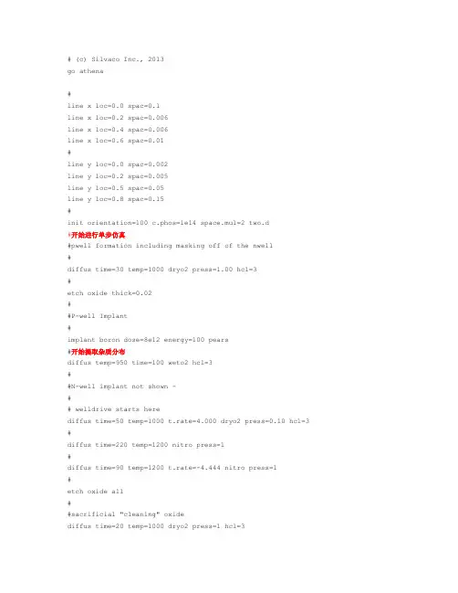
# (c) Silvaco Inc., 2013go athena#line x loc=0.0 spac=0.1line x loc=0.2 spac=0.006line x loc=0.4 spac=0.006line x loc=0.6 spac=0.01#line y loc=0.0 spac=0.002line y loc=0.2 spac=0.005line y loc=0.5 spac=0.05line y loc=0.8 spac=0.15#init orientation=100 c.phos=1e14 space.mul=2 two.d#开始进行单步仿真#pwell formation including masking off of the nwell#diffus time=30 temp=1000 dryo2 press=1.00 hcl=3#etch oxide thick=0.02##P-well Implant#implant boron dose=8e12 energy=100 pears#开始提取杂质分布diffus temp=950 time=100 weto2 hcl=3##N-well implant not shown -## welldrive starts herediffus time=50 temp=1000 t.rate=4.000 dryo2 press=0.10 hcl=3 #diffus time=220 temp=1200 nitro press=1#diffus time=90 temp=1200 t.rate=-4.444 nitro press=1#etch oxide all##sacrificial "cleaning" oxidediffus time=20 temp=1000 dryo2 press=1 hcl=3etch oxide all##gate oxide grown here:-diffus time=11 temp=925 dryo2 press=1.00 hcl=3## Extract a design parameterextract name="gateox" thickness oxide mat.occno=1 x.val=0.05##vt adjust implantimplant boron dose=9.5e11 energy=10 pearson#depo poly thick=0.2 divi=10##from now on the situation is 2-D#etch poly left p1.x=0.35#method fermi compressdiffuse time=3 temp=900 weto2 press=1.0#implant phosphor dose=3.0e13 energy=20 pearson#depo oxide thick=0.120 divisions=8#etch oxide dry thick=0.120#implant arsenic dose=5.0e15 energy=50 pearson#method fermi compressdiffuse time=1 temp=900 nitro press=1.0## pattern s/d contact metaletch oxide left p1.x=0.2deposit alumin thick=0.03 divi=2etch alumin right p1.x=0.18# Extract design parameters# extract final S/D Xjextract name="nxj" xj silicon mat.occno=1 x.val=0.1 junc.occno=1# extract the N++ regions sheet resistanceextract name="n++ sheet rho" sheet.res material="Silicon" mat.occno=1 x.val=0.05 region.occno=1# extract the sheet rho under the spacer, of the LDD regionextract name="ldd sheet rho" sheet.res material="Silicon" \mat.occno=1 x.val=0.3 region.occno=1# extract the surface conc under the channel.extract name="chan surf conc" surf.conc impurity="Net Doping" \material="Silicon" mat.occno=1 x.val=0.45# extract a curve of conductance versus bias.extract start material="Polysilicon" mat.occno=1 \bias=0.0 bias.step=0.2 bias.stop=2 x.val=0.45extract done name="sheet cond v bias" \curve(bias,1dn.conduct material="Silicon" mat.occno=1 region.occno=1)\outfile="extract.dat"# extract the long chan Vtextract name="n1dvt" 1dvt ntype vb=0.0 qss=1e10 x.val=0.49structure mirror rightelectrode name=gate x=0.5 y=0.1electrode name=source x=0.1electrode name=drain x=1.1electrode name=substrate backsidestructure outfile=mos1ex01_0.str# plot the structuretonyplot mos1ex01_0.str -set mos1ex01_0.set############# Vt Test : Returns Vt, Beta and Theta ################go atlas# set material modelsmodels cvt srh printcontact name=gate n.polyinterface qf=3e10method newtonsolve init# Bias the drainsolve vdrain=0.1# Ramp the gatelog outf=mos1ex01_1.log mastersolve vgate=0 vstep=0.25 vfinal=3.0 name=gatesave outf=mos1ex01_1.str# plot resultstonyplot mos1ex01_1.log -set mos1ex01_1_log.set# extract device parametersextract name="nvt" (xintercept(maxslope(curve(abs(v."gate"),abs(i."drain")))) \ - abs(ave(v."drain"))/2.0)extract name="nbeta" slope(maxslope(curve(abs(v."gate"),abs(i."drain")))) \ * (1.0/abs(ave(v."drain")))extract name="ntheta" ((max(abs(v."drain")) * $"nbeta")/max(abs(i."drain"))) \ - (1.0 / (max(abs(v."gate")) - ($"nvt")))quit1、画出结构图,进行单步仿真,代码翻译(第7次实验)2、对比实验(第8次实验)注意:对比仿真时只能改变一个参数,其它参数要恢复到参考代码原始值。