CR6848 电源IC规格书
- 格式:pdf
- 大小:1.36 MB
- 文档页数:11
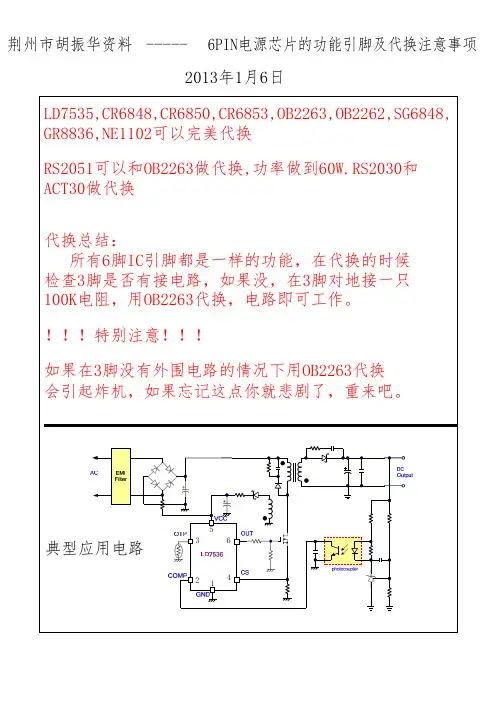
荆州市胡振华资料----- 6PIN电源芯片的功能引脚及代换注意事项2013年1月6日LD7535,CR6848,CR6850,CR6853,OB2263,OB2262,SG6848,GR8836,NE1102可以完美代换RS2051可以和OB2263做代换,功率做到60W.RS2030和ACT30做代换代换总结:所有6脚IC引脚都是一样的功能,在代换的时候检查3脚是否有接电路,如果没,在3脚对地接一只100K电阻,用OB2263代换,电路即可工作。
特别注意如果在3脚没有外围电路的情况下用OB2263代换会引起炸机,如果忘记这点你就悲剧了,重来吧。
典型应用电路53 6 2 1 44321TOP MARK YYWWPP567 8 pp231 65 4 YW P 36引脚功能DIP-8 (TOP VIEW)SOT-26 (TOP VIEW)OUTVCCCSGND COMP OTPPin DescriptionsPIN SOT-26 PIN DIP-8名称功能18GNDGround27COMPVoltage feedback pin (same as the COMP pin in UC384X). Connect a photo-coupler to close the control loop and achieve the regulation.35OTPPull this pin below 0.95V to shutdown the controller into latch mode until the ACresume power-on. Connecting this pin to ground with NTC will achieve OTP protection. Keep this pin float to disable the latch protection.4 4 CS Current sense pin, connect it to sense the MOSFET current5 2 VCC Supply voltage pin61OUTGate drive output to drive the external MOSFETO U TG N DC O M PN CV C CN CO T PC S芯片内部方框图Fig. 15Fig. 17A pull-high resistor is embedded internally and can be eliminated externally.A 230nS leading-edge blanking (LEB) time is included in the input of CS pin to prevent the false-trigger from the current spike. In the low power application, if the total pulse width of the turn-on spikes is less than 230nS and the negative spike on the CS pin below -0.3V, the R-C filter is free to eliminate. (As shown in Fig.16).However, the total pulse width of the turn-on spike is determined according to output power, circuit design and PCB layout. It is strongly recommended to adopt a smaller R-C filter (as shown in Fig. 17) for larger power application to avoid the CS pin being damaged by the negative turn-on spike.Output Stage and Maximum Duty-CycleAn output stage of a CMOS buffer, with typical 300mA driving capability, is incorporated to drive a power MOSFET directly. And the maximum duty-cycle of LD7536 is limited to 75% to avoid the transformer saturation.Voltage Feedback LoopThe voltage feedback signal is provided from the TL431 at the secondary side through the photo-coupler to the COMP pin of the LD7536. Similar to UC3842, the LD7536 would carry a diode voltage offset at the stage to feed the voltage divider at the ratio of RA and RB, that is,Fig. 16V -(PWM COMPARATOR ) =RBRA + RB⨯ (V COMP - V F )C5F1 3.15A/250V LL1 120uH L2 22mH330P/1206 R3R12.2MEG/1206R22.2MEG/1206NCX1 0.22uFBR1KBP206C4 82uF/400VR9 51K/1206 C6NC102pF/1206 R10T1ARM8C151R/1206D5 20120C7 470uF/25VC8470uF/25VC10 104P/080519V / 2.1A+VoR5620K/1206D1R6620K/120651k/1206R11 22R/1206D2 PR1007U1AR32DZ2/6.8VZENER1 RTNR40/0805 GS1002FLSMDR31330/08055.6k/0805T1BC11 4.7u/50VC12104P/08052 COMP5 VCCOUT 6R12B 10R/0805D6 D4148R12Q12SK3562IC432R251K/0805R29 4.3k/0805C16 R2862K/0805R30 /0805PC817B3.3nF/0805 LD7536CS 4200R/0805C13 3 OTPGNDR13100R/0805 C13 1 100P/0805C14100PF/0805R16A R16 1.4/1206 R16B 1.4/1206CY1 1.4/1206102P473p/0805 --- 40W (19V /2.1A )典型电源适配器电路图。

液晶常⽤电源管理芯⽚1200AP40 1200AP60、1203P60200D6、203D6 DAP8A 可互代203D6/1203P6 DAP8A2S0680 2S08803S0680 3S08805S0765 DP104、DP7048S0765C DP704加24V得稳压⼆极管ACT4060 ZA3020LV/MP1410/MP9141ACT4065 ZA3020/MP1580ACT4070 ZA3030/MP1583/MP1591MP1593/MP1430ACT6311 LT1937ACT6906 LTC3406/A T1366/MP2104AMC2576 LM2576AMC2596 LM2596AMC3100 LTC3406/AT1366/MP2104AMC34063A AMC34063AMC7660 AJC1564AP8012 VIPer12AAP8022 VIPer22ADAP02 可⽤SG5841 /SG6841代换DAP02ALSZ SG6841DAP02ALSZ SG6841DAP7A、DP8A 203D6、1203P6DH321、DL321 Q100、DM0265RDM0465R DM/CM0565RDM0465R/DM0565R ⽤cm0565r代换(取掉4脚得稳压⼆极管) DP104 5S0765 DP704 5S0765DP706 5S0765DP804 DP904FAN7601 LAF0001LD7552 可⽤SG6841代(改4脚电阻)LD7575PS 203D6改1脚100K电阻为24KOB2268CP OB2269CPOB2268CP SG6841改4脚100K电阻为2047KOCP1451 TL1451/BA9741/SP9741/AP200OCP2150 LTC3406/AT1366/MP2104OCP2160 LTC3407OCP2576 LM2576OCP3601 MB3800OCP5001 TL5001OMC2596 LM2596/AP1501PT1301 RJ9266PT4101 AJC1648/MP3202PT4102 LT1937/AJC1896/AP1522/RJ9271/MP1540SG5841SZ SG6841DZ/SG6841DSM9621 RJ9621/AJC1642SP1937 LT1937/AJC1896/AP1522/RJ9271/MP1540STRG5643D STRG5653D、STRG8653DTEA1507 TEA1533TEA1530 TEA1532对应引脚功能接⼊THX202H TFC719THX203H TFC718STOP246Y TOP247YV A7910 MAX1674/75 L6920 AJC1610VIPer12A VIPer22A[audio01]ICE2A165(1A/650V、31W);ICE2A265(2A/650V、52W);ICE2B0565(0、5A/650V、23W):ICE2B165(1A/650V、31W);ICE2B265(2A/650V、52W);ICE2A180(1A/800V、29W);ICE2A280(2A/800、50W)、KA5H0365R, KA5M0365R, KA5L0365R, KA5M0365RN# u) t! u1 W1 B) R, PKA5L0365RN, KA5H0380R, KA5M0380R, KA5L0380R1、KA5Q1265RF/RT(⼤⼩两种体积)、KA5Q0765、FSCQ1265RT、KACQ1265RF、FSCQ0765RT、FSCQ1565Q这就是⼀类得,这些型号得引脚功能全都⼀样,只就是输出功率不⼀样。

CR6848Novel Low Cost Green-Power PWM Controller Featuresz Low Cost, PWM&PFM&CRMz Low Start-up Current (about 10µA)z Low Operating Current (about 2mA) z Current Mode Operationz Under Voltage Lockout (UVLO)z Built-in Synchronized SlopeCompensationz Programmable PWM Frequencyz Leading edge Blanking on Sense input z Constant output power limiting foruniversal AC inputz Cycle-by-cycle current limitingz Clamped gate output voltage 16.5Vz Over voltage protect 26.7Vz High-Voltage CMOS Process with ESD z SOT-23-6L、SOP-8 & DIP-8 Pb-Free Packagingz Compatible with SG5701 & SG5848 & LD7535 &OB22632/63Applicationsz Switching AC/DC Adaptor z Battery Charger z Open Frame Switching Power Supply z 384X ReplacementGeneral DescriptionThe CR6848 is a highly integrated low cost current mode PWM controller, which is ideal for small power current mode of offline AC-DC fly-back converter applications. Making use of external resistors, the IC changes the operating frequency and automatically enters the PFM/CRM under light-load/zero-load conditions. This can minimize standby power consumption and achieve green-power functions. With a very low start-up current, the CR6848 could use a large value start-up resistor (1.5Mohm). Built-in synchronized slope compensation enhances the stability of the system and avoids sub-harmonic oscillation. Dynamic peak limiting circuit minimizes output power change caused by delay time of the system over a universal AC input range. Leading edge blanking circuit on current sense input could remove the signal glitch due to snubber circuit diode reverse recovery and thus greatly reduces the external component count and system cost in the design. Pulse-by-pulse current limiting ensures safe operation even during short-circuit.The CR6848 offers more protection like OVP (Over Voltage Protection) and OCP (Over current protection). The CR6848’s output driver is clamped to maximum 16.5Vto protect the power MOSFET. Excellent EMI performance is achieved soft switching control at the totem pole gate driver output. CR6848 is offered in SOT-23-6, SOP-8 and DIP-8 packages.Dec, 2006 V1.5 1/14Block DiagramTYPICAL CHARACTERISTICSVDD startup Current VS TemperatureVDD (OFF) VS TemperatureOVP VS TemperatureDuty cycle VS TemperatureVDD startup Current VS TemperatureVDD Operation Current VS TemperaturePWM frequency VS TemperatureF OSC VS FB CurrentF OSC VS RI pin resistorDec, 2006 V1.5 8/14OPERATION DESCRIPTION Current ModelCompared to voltage model control, current model control has a current feedback loop. When the voltage of the sense resistor peak current of the primary winding reaches the internal setting value V TH , comparator reverse, register reset and power MOSFET cut-off. So that to detect and modulate the peak current cycle by cycle could control the output of the power supply. The current feedback has a good linear modulation rate and a fast input and output dynamic impact avoid the pole that the output filter inductance brings and the second class system descends to first class and so it widens the frequency range and optimizes overload protection and short circuit protection.Startup Current and Under Voltage LockoutThe startup current of CR6848 is set to be very low so that a large value startup resistor can therefore be used to minimize the power loss. For AC to DC adaptor with universal input range design, a 1.5 M Ω, 1/8 W startup resistor and a 10uF/25V VDD hold capacitor could be used.The turn-on and turn-off threshold of the CR6848 is designed to 16.1V/11.1V. During startup, the hold-up capacitor must be charge to 16.1V through the startup resistor. The hysteresis is implemented to prevent the shutdown from the voltage dip during startup.Internal Bias and OSC OperationA resistor connected between RI pin and GND pin set the internal constant current source to charge or discharge the internal fixed cap. The charge time and discharge time determine the internal clock speed and the switching frequency. Increasing the resistance will reduce the value of the input current and reduce the switching frequency. The relationship between RI pin and PWM switching frequency follows the below equation within the RI allowed range.)()(5800kHz K RI F OSC Ω=For example, a 100k Ω resistor RI could generate a 50uA constant current and a 58kHz PWM switching frequency. Thesuggested operating frequency range of CR6848 is within 48KHz to 100KHz.Green Power OperationThe power dissipation of switching mode power supply is very important in zero load or light load condition. The major dissipation result from conduction loss 、switching loss and consume of the control circuit. However, all of them related to the switching frequency. There are many difference topologies has been implemented in different chip. The basic operation theory of all these approaches intended to reduce the switching frequency under light-load or no-load condition.CR6848`s green power function adapts PWM 、PFM and CRM combining modulation. When RI resistor is 100k, the PWM frequency is 58kHz in medium or heavy load operation. Through modifying the pulse width, CR6848 could control output voltage. The current of FB pin increases when the load is in light condition and the internal mode controller enters PFM&PWM when the feedback current is over 0.92mA. The operation frequency of oscillator is to descend gradually. The invariable frequency of oscillator is 11.6kHz when the feedback current is over 1.05mA. To decrease the standby consumption of the power supply , Chip-Rail introduces the Cycle Reset Mode technology ;If the feedback current were over 1.1mA, mode controller of CR6848 would reset internal register all the time and cut off the gate pin, while the output voltage is lower than the set value, it would set register, gate pin operating again. Although the frequency of the internal OSC is invariable, the register would reset some pulses so that the practical frequency is decreased at the gate pin.CR6848 Green-Power FunctionDec, 2006 V1.5 9/14Internal Synchronized Slop Compensation Although there are more advantages of the current mode control than conventional voltage mode control, there are still several drawbacks of peak-sensing current-mode converter. Especially the open loop instability when it operates in higher than 50% of the duty-cycle. CR6848 is introduced an internal slope compensation adding voltage ramp to the current sense input voltage for PWM generation to solve this problem. It improves the close loop stability greatly at CCM, prevents the sub-harmonic oscillation and thus reduces the output ripple voltage.DUTYDUTY DUTYV MAXSLOP ×=×=4389.033.0Current Sensing & Dynamic peak limitingThe current flowing by the power MOSFET comes in to being a voltage V SENSE on the sense pin cycle by cycle, which compares to the internal reference voltage, controls the reverse of the internal register, limits the peak current IMAX of the primary of the transformer. The energy 221MAX I L E ××=deposited by the transformer. So adjusting the R SENSE can set the Max output power of the power supple mode. The current flowing by the power MOSFET has an extra valueD PINT L V I ×=∆ due to the system delay T that the current detected from the sense pin to power MOSFET cut off in the CR6848 (Among these, V IN is the primary winding voltage of the transformer and L P is theprimary wind inductance. IN V ranges from 85VAC to 264V AC. To guarantee the outputpower is a constant for universal input AC voltage, there is a dynamic peak limit circuit to compensate the system delay T that the system delay brings on.Leading-edge Blanking (LEB)Each time the power MOSFET is switched on, a turn-on spike will inevitably occur at the sense pin, which would disturb the internal signal from the sampling of the R SENSE . There is a 300n sec leading edge blanking time built in to avoid the effect of the turn-on spike and the power MOSFET cannot be switched off during this time. So that the conventional external RC filtering on sense input is no longer required.Over Voltage Protection (OVP)There is a 26.7V over-voltage protection circuit in the CR6848 to improve the credibility and extend the life of the chip. The GATE is to shutdown immediately when the voltage of the VDD is over 26.7V and the voltage of VDD is to descend rapidly.Gate Driver & Soft ClampedCR6848’ output designs a totem pole to drive a periphery power MOSFET. The dead time is introduced to minimize the transfixion current when the output is drove. The NMOS is shut off when the other NMOS is turned on. The clamp technology is introduced to protect the periphery power MOSFET from breaking down.。
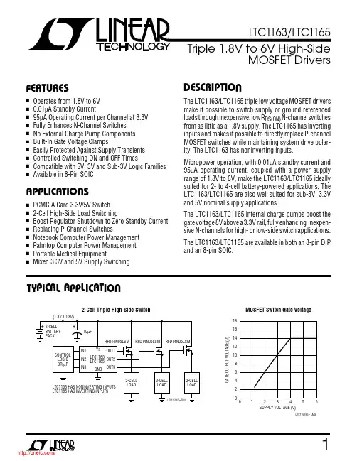
MOSFET DriversSFEATUREs Operates from 1.8V to 6Vs0.01µA Standby Currents95µA Operating Current per Channel at 3.3Vs Fully Enhances N-Channel Switchess No External Charge Pump Componentss Built-In Gate Voltage Clampss Easily Protected Against Supply Transientss Controlled Switching ON and OFF Timess Compatible with 5V, 3V and Sub-3V Logic Families s Available in 8-Pin SOIC D UESCRIPTIOThe LTC1163/LTC1165 triple low voltage MOSFET drivers make it possible to switch supply or ground referenced loads through inexpensive, low R DS(ON) N-channel switches from as little as a 1.8V supply. The LTC1165 has inverting inputs and makes it possible to directly replace P-channel MOSFET switches while maintaining system drive polar-ity. The LTC1163 has noninverting inputs. Micropower operation, with 0.01µA standby current and 95µA operating current, coupled with a power supply range of 1.8V to 6V, make the LTC1163/LTC1165 ideally suited for 2- to 4-cell battery-powered applications. The LTC1163/LTC1165 are also well suited for sub-3V, 3.3V and 5V nominal supply applications.The LTC1163/LTC1165 internal charge pumps boost the gate voltage 8V above a 3.3V rail, fully enhancing inexpen-sive N-channels for high- or low-side switch applications. The LTC1163/LTC1165 are available in both an 8-pin DIP and an 8-pin SOIC.SUPPLY VOLTAGE (V)GATEOUTPUTVOLTAGE(V)26810418LTC1163/65 • TA02426121416315MOSFET Switch Gate Voltage 2-Cell Triple High-Side SwitchU SA OPPLICATIs PCMCIA Card 3.3V/5V Switchs2-Cell High-Side Load Switchings Boost Regulator Shutdown to Zero Standby Currents Replacing P-Channel Switchess Notebook Computer Power Managements Palmtop Computer Power Managements Portable Medical Equipments Mixed 3.3V and 5V Supply SwitchingUA OPPLICATITYPICAL12LTC1163/LTC1165SYMBOL PARAMETER CONDITIONSMIN TYP MAXUNITS I QQuiescent Current OFFV S = 1.8V, V IN1 = V IN2 = V IN3 = V OFF (Note 1,2)0.011µA V S = 3.3V, V IN1 = V IN2 = V IN3 = V OFF (Note 1,2)0.011µA V S = 5V, V IN1 = V IN2 = V IN3 = V OFF (Note 1,2)0.011µA Quiescent Current ONV S = 1.8V, V IN = V ON (Note 2,3)60120µA V S = 3.3V, V IN = V ON (Note 2,3)95200µA V S = 5V, V IN = V ON (Note 2,3)180400µA V INH Input High Voltage 1.8V < V S < 2.7V q 80% × V S V 2.7V < V S < 6V q 70% × V SVV INL Input Low Voltage 1.8V < V S < 6V q 15% × V SV I IN Input Current 0V ≤ V IN ≤ V Sq±1µA C IN Input Capacitance 5pF V GATE – V SGate Voltage Above SupplyV S = 1.8V, V IN = V ON (Note 2)q 3.5 4.1 6.0V V S = 2V, V IN = V ON (Note 2)q 4.0 4.6 7.0V V S = 2.2V, V IN = V ON (Note 2)q 4.5 5.2 8.0V V S = 3.3V, V IN = V ON (Note 2)q 6.08.0 9.5V V S = 5V, V IN = V ON (Note 2)q5.09.013.0V t ONTurn-ON TimeV S = 3.3V, C GATE = 1000pF Time for V GATE > V S + 1V 40120400µs Time for V GATE > V S + 2V 60180600µs V S = 5V, C GATE = 1000pF Time for V GATE > V S + 1V 3095300µs Time for V GATE > V S + 2V40130400µsA UG WA WUW A R BSOLUTEXI TI SOperating Temperature RangeLTC1163C/LTC1165C........................... 0°C to 70°C Storage Temperature Range................ –65°C to 150°C Lead Temperature (Soldering, 10 sec)................. 300°CSupply Voltage ......................................................... 7V Any Input Voltage.......................... 7V to (GND – 0.3V)Any Output Voltage....................... 20V to (GND – 0.3V)Current (Any Pin)................................................. 50mAWUUPACKAGE/ORDER I FOR ATIOV S = 1.8V to 6V, T A = 25°C, unless otherwise noted.ELECTRICAL C C HARA TERISTICSLTC1163C/LTC1165C /3LTC1163/LTC1165ELECTRICAL C C HARA TERISTICSV S = 1.8V to 6V, T A = 25°C, unless otherwise noted.SYMBOL PARAMETER CONDITIONSMIN TYP MAX UNITSt OFFTurn-OFF TimeV S = 3.3V, C GATE = 1000pFTime for V GATE < 0.5V 2065200µs V S = 5V, C GATE = 1000pF Time for V GATE < 0.5V1545150µsLTC1163C/LTC1165C The q denotes specifications which apply over the full operating temperature range.Note 1: Quiescent current OFF is for all channels in OFF condition.Note 2: LTC1163: V OFF = 0V, V ON = V S . LTC1165: V OFF = V S , V ON = 0V Note 3: Quiescent current ON is per driver and is measured independently.Gate Voltage Above SupplySupply Current per Driver ONStandby Supply CurrentC C HARA TERISTICSU WA TYPICAL PERFOR CE SUPPLY VOLTAGE (V)0SU P P L Y C U R R E N T (µA )5 4 3 2 1 0 –11234LTC1163/65 • TPC0156SUPPLY VOLTAGE (V)V G A T E – V S (V )1210 8 6 4 2 01234LTC1163/65 • TPC0356SUPPLY VOLTAGE (V)0S U PP L Y C U R R E N T (µA )600 500 400 300 200 100 01234LTC1163/65 • TPC0256Input Threshold VoltageTurn-ON TimeTurn-OFF TimeSUPPLY VOLTAGE (V)0I N P U T T H R E S H O L DV O L T A G E (V )65 4 3 2 1 01234LTC1163/65 • T PC0456SUPPLY VOLTAGE (V)T U R N -O N T IM E (µs )600500 400 300 200 100 01234LTC1163/65 • TPC0556SUPPLY VOLTAGE (V)0T U R N -OF F T I M E (µs )300250 200 150 100 50 01234LTC1163/65 • TA06564LTC1163/LTC1165C C HARA TERISTICSU WA TYPICAL PERFOR CE PI FU CTIO SU U U Input PinsThe LTC1163 is noninverting; i.e., the MOSFET gate is driven above the supply when the input pin is held high.The LTC1165 is inverting and drives the MOSFET gate high when the input pin is held low. The inverting inputs of the LTC1165 allow P-channel switches to be replaced by lower resistance/cost N-channel switches while maintain-ing system drive polarity.The LTC1163/LTC1165 logic inputs are high impedance CMOS gates with ESD protection diodes to ground and therefore should not be forced below ground. The inputs can however, be driven above the power supply rail as there are no clamping diodes connected between the input pins and supply pin. This facilitates operation in mixed 5V/3V systems.Output PinsThe output pin is either driven to ground when the switch is turned OFF or driven above the supply rail when the switch is turned ON. The output is clamped to about 14V above ground by a built-in Zener clamp. This pin has a relatively high impedance when driven above the rail (the equivalent of a few hundred k Ω). Care should be taken to minimize any loading of this pin by parasitic resistance to ground or supply.Supply PinA 150Ω resistor should be inserted in series with the ground pin or supply pin if negative supply voltage tran-sients are anticipated. This will limit the current flowing from the power source into the LTC1163/LTC1165 to tens of milliamps during reverse battery conditions.OPERATIOUThe LTC1163/LTC1165 are triple micropower MOSFET drivers designed for operation over the 1.8V to 6V supply range and include the following functional blocks:3V Logic Compatible InputsThe LTC1163/LTC1165 inputs have been designed to accommodate a wide range of 3V and 5V logic families.The input threshold voltage is set at roughly 50% of the supply voltage and approximately 200mV of input hyster-esis is provided to ensure clean switching.The input enables all of the following circuit blocks: the bias generator, the high frequency oscillator and gate charge pump. Therefore, when the input is turned off, the entire circuit powers down and the supply current drops below 1µA.Standby Supply CurrentTEMPERATURE (°C)0S U P P L Y C U R R E N T (µA )5 4 3 2 1 0 –110203040LTC1163/65 • TPC07506070MOSFET Gate Drive CurrentGATE VOLTAGE ABOVE SUPPLY (V)1G A T E D R I V E C U R R E N T (µA )1010010004680.1210LTC1163/65 • TPC09Supply Current per Driver ONTEMPERATURE (°C)0S U P P L Y C U R R E N T (µA )300 250200150 100 50 010203040LTC1163/65 • TPC08506070/5LTC1163/LTC1165OPERATIOUGate Charge PumpGate drive for the power MOSFET is produced by an internal charge pump circuit which generates a gate volt-age substantially higher than the power supply voltage.The charge pump capacitors are included on chip and therefore no external components are required to generate gate drive.Controlled Gate Rise and Fall TimesWhen the input is switched ON and OFF, the gate is charged by the internal charge pump and discharged in a controlled manner. The charge and discharge rates have been set to minimize RFI and EMI emissions.BLOCK DIAGRA W(One Channel)APPLICATIO S I FOR ATIOW UU U Logic-Level MOSFET SwitchesThe LTC1163/LTC1165 are designed to operate with logic-level N-channel MOSFET switches. Although there is some variation among manufacturers, logic-level MOSFET switches are typically rated with V GS = 4V with a maximum continuous V GS rating of ±10V. R DS(ON) and maximum V DS ratings are similar to standard MOSFETs and there is generally little price differential. Logic-level MOSFETs are frequently designated by an “L” and are usually available in surface mount packaging. Some logic-level MOSFETs are rated with V GS up to ±15V and can be used in applications which require operation over the entire 1.8V to 6V range.Powering Large Capacitive LoadsElectrical subsystems in portable battery-powered equip-ment are typically bypassed with large filter capacitors to reduce supply transients and supply induced glitching. If not properly powered however, these capacitors may themselves become the source of supply glitching.For example, if a 100µF capacitor is powered through a switch with a slew rate of 0.1V/µs, the current during start-up is:I START = C(∆V/∆t)= (100 × 10–6)(1 × 10⁵)= 10AObviously, this is too much current for the regulator (or output capacitor) to supply and the output will glitch by as much as a few volts.The startup current can be substantially reduced by limit-ing the slew rate at the gate of an N-channel as shown in Figure 1. The gate drive output of the LTC1163/LTC1165is passed through a simple RC network, R1 and C1, which substantially slows the slew rate of the MOSFET gate to approximately 1.5 × 10⁻⁴V/µs. Since the MOSFET is operating as a source follower, the slew rate at the source is essentially the same as that at the gate, reducing the startup current to approximately 15mA which is easilyGATEINPUT6LTC1163/LTC1165APPLICATIO S I FOR ATIOW UU U Figure 1. Powering a Large Capacitive Loadon a 3.3V supply which is compatible with 5V TTL and CMOS logic. (The LTC1163/LTC1165 cannot however, be driven by 3V logic when powered from a 5V supply because the threshold is approximately 2.5V.)TYPICAL APPLICATIO SUPCMCIA Card 3.3V/5V V CC SwitchNOTE: USE LTC1163 WITH NONINVERTING PCMCIA CONTROLLERSmanaged by the system regulator. R2 is required to eliminate the possibility of parasitic MOSFET oscillations during switch transitions. It is a good practice to isolate the gates of paralleled MOSFETs with 1k resistors to decrease the possibility of interaction between switches.Mixed 5V/3V SystemsBecause the input ESD protection diodes are referenced to ground instead of the supply pin, it is possible to drive the LTC1163/LTC1165 inputs from 5V CMOS or TTL logic even though the LTC1163/LTC1165 are powered from a 3.3V supply as shown in Figure 2. The input threshold voltage is approximately 50% of the supply voltage or 1.6VReverse Battery ProtectionThe LTC1163/LTC1165 can be protected against reverse battery conditions by connecting a 150Ω resistor in series with the ground pin or supply pin. The resistor limits the supply current to less than 24mA with –3.6V applied.Because the LTC1163/LTC1165 draw very little currentwhile in normal operation, the drop across the resistor is minimal. The 3.3V µP (or control logic) can be protected by adding 10k resistors in series with the input pins.Figure 2. Direct Interface to 5V LogicV IN/7LTC1163/LTC1165Information furnished by Linear Technology Corporation is believed to be accurate and reliable.However, no responsibility is assumed for its use. Linear Technology Corporation makes no represen-tation that the interconnection of its circuits as described herein will not infringe on existing patent rights.TYPICAL APPLICATIO SU2-Cell to 3.3V, 5V and 12V High-Side Switch/Converterwith 0.01µA Standby Current3.3VµF3.3VUltra-Low Drop Triple 3.3V High-Side SwitchPCMCIA Card Socket V PP Switch/ReglatorV CC MMDF3N02HDPP = 0V, 3.3V,EN0 0 1 0 1EN1 0 0 1 1OUTPUT 0V 12V V CC HI-Z8LTC1163/LTC1165Linear Technology Corporation1630 McCarthy Blvd., Milpitas, CA 95035-7487(408) 432-1900 qFAX : (408) 434-0507 qTELEX : 499-3977© U SA OPPLICATITYPICAL S8 Package 8-Lead Plastic SOICPACKAGE DESCRIPTIO U3-Cell to 3.3V Ultra-Low Drop Regulator with 2 Ramped SwitchesµFMixed Voltage High- and Low-Side SwitchesN8 Package 8-Lead Plastic DIPDimensions in inches (millimeters) unless otherwise noted.–0.3818.2550.053 – 0.069 BSC/分销商库存信息:LINEAR-TECHNOLOGYLTC1163CS8#PBF LTC1165CN8LTC1165CN8#PBF LTC1165CS8LTC1165CS8#PBF LTC1163CS8LTC1165CS8#TR LTC1165CS8#TRPBF LTC1163CS8#TR LTC1163CS8#TRPBF LTC1163CN8LTC1163CN8#PBF。
CommandsDESELECT The DESELT (DES) command (CS# HIGH) prevents new commands from being execu-ted by the DRAM. Operations already in progress are not affected.NO OPERATION The NO OPERATION (NOP) command (CS# LOW) prevents unwanted commands from being registered during idle or wait states. Operations already in progress are not affec-ted.ZQ CALIBRATION LONGThe ZQ CALIBRATION LONG (ZQCL) command is used to perform the initial calibra-tion during a power-up initialization and reset sequence (see Figure 50 (page 137)).This command may be issued at any time by the controller, depending on the systemenvironment. The ZQCL command triggers the calibration engine inside the DRAM. Af-ter calibration is achieved, the calibrated values are transferred from the calibration en-gine to the DRAM I/O, which are reflected as updated R ON and ODT values.The DRAM is allowed a timing window defined by either t ZQinit or t ZQoper to performa full calibration and transfer of values. When ZQCL is issued during the initializationsequence, the timing parameter t ZQinit must be satisfied. When initialization is com-plete, subsequent ZQCL commands require the timing parameter t ZQoper to be satis-fied.ZQ CALIBRATION SHORTThe ZQ CALIBRATION SHORT (ZQCS) command is used to perform periodic calibra-tions to account for small voltage and temperature variations. A shorter timing windowis provided to perform the reduced calibration and transfer of values as defined by tim-ing parameter t ZQCS. A ZQCS command can effectively correct a minimum of 0.5% R ONand R TT impedance error within 64 clock cycles, assuming the maximum sensitivitiesspecified in DDR3L 34 Ohm Output Driver Sensitivity (page 69).ACTIVATEThe ACTIVATE command is used to open (or activate) a row in a particular bank for asubsequent access. The value on the BA[2:0] inputs selects the bank, and the addressprovided on inputs A[n:0] selects the row. This row remains open (or active) for accessesuntil a PRECHARGE command is issued to that bank.A PRECHARGE command must be issued before opening a different row in the samebank.READThe READ command is used to initiate a burst read access to an active row. The addressprovided on inputs A[2:0] selects the starting column address, depending on the burstlength and burst type selected (see Burst Order table for additional information). Thevalue on input A10 determines whether auto precharge is used. If auto precharge is se-lected, the row being accessed will be precharged at the end of the READ burst. If autoprecharge is not selected, the row will remain open for subsequent accesses. The valueon input A12 (if enabled in the mode register) when the READ command is issued de-termines whether BC4 (chop) or BL8 is used. After a READ command is issued, theREAD burst may not be interrupted.Table 72: READ Command SummaryWRITEThe WRITE command is used to initiate a burst write access to an active row. The valueon the BA[2:0] inputs selects the bank. The value on input A10 determines whether autoprecharge is used. The value on input A12 (if enabled in the MR) when the WRITE com-mand is issued determines whether BC4 (chop) or BL8 is used.Input data appearing on the DQ is written to the memory array subject to the DM inputlogic level appearing coincident with the data. If a given DM signal is registered LOW,the corresponding data will be written to memory. If the DM signal is registered HIGH,the corresponding data inputs will be ignored and a WRITE will not be executed to thatbyte/column location.Table 73: WRITE Command SummaryPRECHARGEThe PRECHARGE command is used to de-activate the open row in a particular bank orin all banks. The bank(s) are available for a subsequent row access a specified time (t RP)after the PRECHARGE command is issued, except in the case of concurrent auto pre-charge. A READ or WRITE command to a different bank is allowed during a concurrentauto precharge as long as it does not interrupt the data transfer in the current bank anddoes not violate any other timing parameters. Input A10 determines whether one or allbanks are precharged. In the case where only one bank is precharged, inputs BA[2:0] se-lect the bank; otherwise, BA[2:0] are treated as “Don’t Care.”After a bank is precharged, it is in the idle state and must be activated prior to any READor WRITE commands being issued to that bank. A PRECHARGE command is treated asa NOP if there is no open row in that bank (idle state) or if the previously open row isalready in the process of precharging. However, the precharge period is determined bythe last PRECHARGE command issued to the bank.REFRESHThe REFRESH command is used during normal operation of the DRAM and is analo-gous to CAS#-before-RAS# (CBR) refresh or auto refresh. This command is nonpersis-tent, so it must be issued each time a refresh is required. The addressing is generated bythe internal refresh controller. This makes the address bits a “Don’t Care” during a RE-FRESH command. The DRAM requires REFRESH cycles at an average interval of 7.8μs(maximum when T C 85°C or 3.9μs maximum when T C 95°C). The REFRESH periodbegins when the REFRESH command is registered and ends t RFC (MIN) later.To allow for improved efficiency in scheduling and switching between tasks, some flexi-bility in the absolute refresh interval is provided. A maximum of eight REFRESH com-mands can be posted to any given DRAM, meaning that the maximum absolute intervalbetween any REFRESH command and the next REFRESH command is nine times themaximum average interval refresh rate. Self refresh may be entered with up to eight RE-FRESH commands being posted. After exiting self refresh (when entered with postedREFRESH commands), additional posting of REFRESH commands is allowed to the ex-tent that the maximum number of cumulative posted REFRESH commands (both pre-and post-self refresh) does not exceed eight REFRESH commands.At any given time, a maximum of 16 REFRESH commands can be issued within2 x t REFI.Figure 42: Refresh ModeDon’t CareIndicates break in time scaleCKCK#Command CKE AddressA10BA[2:0]DQ 4DM 4DQS, DQS#4Notes:1.NOP commands are shown for ease of illustration; other valid commands may be possi-ble at these times. CKE must be active during the PRECHARGE, ACTIVATE, and REFRESH commands, but may be inactive at other times (see Power-Down Mode (page 187)).2.The second REFRESH is not required, but two back-to-back REFRESH commands are shown.3.“Don’t Care” if A10 is HIGH at this point; however, A10 must be HIGH if more than one bank is active (must precharge all active banks).4.For operations shown, DM, DQ, and DQS signals are all “Don’t Care”/High-Z.5.Only NOP and DES commands are allowed after a REFRESH command and until t RFC(MIN) is satisfied.SELF REFRESHThe SELF REFRESH command is used to retain data in the DRAM, even if the rest of the system is powered down. When in self refresh mode, the DRAM retains data without ex-ternal clocking. Self refresh mode is also a convenient method used to enable/disable the DLL as well as to change the clock frequency within the allowed synchronous oper-ating range (see Input Clock Frequency Change (page 129)). All power supply inputs (including V REFCA and V REFDQ ) must be maintained at valid levels upon entry/exit and during self refresh mode operation. V REFDQ may float or not drive V DDQ /2 while in self refresh mode under the following conditions:•V SS < V REFDQ < V DD is maintained•V REFDQ is valid and stable prior to CKE going back HIGH•The first WRITE operation may not occur earlier than 512 clocks after V REFDQ is valid •All other self refresh mode exit timing requirements are met。
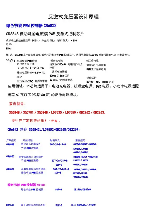
反激式变压器设计原理绿色节能PWM 控制器CR68XXCR6848低功耗的电流模PWM 反激式控制芯片成都启达科技有限公司 联系人:陈金元 TEL: 电话/传真:・218 电邮::MSN:概 述:CR6848是一款高集成度.低功耗的电流模PWM 控制芯片,适用于离线式AC-DC 反激拓扑的小功 率电源模块。
极少的外围元件欠压锁定(12.1V~16.1V) 输出电压钳位(16.5V) 软驱动过压保护(27V) 片内自带前沿消隐(30OnS) 内建同步斜坡补偿周期电流限制200OV 的ESD 保护 60瓦以下的反激电源应用领域:本芯片适用于:电池充电器、机顶盒电源、DVD 电源、小功率电源适配 器等60瓦以下(包括60瓦)的反激电源模块。
兼容型号:SG6848∕SG5701∕SG5848∕LD7535∕LD7550∕OB2262∕OB2263o原生产厂家现货热销!・218,。
CR6842 兼容 SG6842J/LD7552/OB2268/OB2269。
绿色节能PWM 控制器AC-DC绿色节能PWM 控制器SOP-8 OB2268/OB2269特点:电流模式PWM 控制 低启动电流低工作电流 产品型号功能描述 封装形式 兼容型号CR6848低成本小功率绿色 SOT-26/DIP-8SG6848/SG5701/SG5848 节能PWM 控制器LD7535/LD7550OB2262/OB2263CR6850新型低成本小功率绿色SG6848^G5701∕SG5⅛48节能PWM 控制器SOT-26/DIP-8LD7535/LD7550SOP-8 OB2262/OB2263 CR6851具有频率抖动的低成本 SOT-26/DIP-8 SG6848/SG5701/SG5848 绿色节能PWM 控制器SOP-8LD7535/LD755OB2262/OB2263CR6842 具有频率抖动的大功能兼容 SG6842J/LD7552DIP-8额定输出功率限制PWM 工作频率可调过载保护SoT23∙6L ∖ DIP8 封装CR5842具有频率抖动的多保护功能DIP-8大功率绿色节能PWM控制器SOP-8CR6505半桥ATX电源PWM控制器DIP-16兼容VVT7514, AT2005CR6515半桥ATX电源PVVM控制器+TL43[DIP-20兼容SG6105CR6561有源PFC控制器DIP-8x SOP-8(FlybaCk TranSfOrmer DeSign TheOry)第一节.概述.反激式(FIybaCk)转换器乂称单端反激式或,z Buck-BOOSt ZZ转换器•因其输出端在原边绕组断开电源时获得能量故而得名•离线型反激式转换器原理图如图・一、反激式转换器的优点有:1.电路简单,能高效提供多路直流输出,因此适合多组输出要求.2.转换效率高,损失小.3.变压器匝数比值较小・4.输入电压在很大的范圉内波动时,仍可有较稳定的输出,IJ前已可实现交流输入在85~265V间•无需切换而达到稳定输出的要求・二、反激式转换器的缺点有:1.输出电压中存在较大的纹波,负载调整精度不高,因此输出功率受到限制,通常应用于150W以下.2.转换变压器在电流连续(CCH)模式下工作时,有较大的直流分量,易导致磁芯饱和,所以必须在磁路中加入气隙,从而造成变压器体积变大・3.变压器有直流电流成份,且同时会工作于CCM / DCM两种模式,故变压器在设计时较困难,反复调整次数较顺向式多,迭代过程较复杂.第二节∙工作原理在图1所示隔离反驰式转换器(The isolated flyback COnVerter)中,变压器"T "有隔离与扼流之双重作用.因此"T "乂称为TranSfOrmer- choke.电路的匸作原理如下:当开关晶体管Tr ton时,变压器初级NP有电流Ip,并将能量储存于其中(E = L P l P / 2). 由于NP与NS极性相反,此时二极管D反向偏压而截止,无能量传送到负载.当开关Tr Off时,由楞次定律:(e = -N∆Φ∕ΔT)可知,变压器原边绕组将产生一反向电势,此时二极管D正向导通,负载有电流IL流通.反激式转换器之稳态波形如图2.由图可知,导通时间J的大小将决定Ip、VCe的幅值:VCe αas = VI X / I-D IiSV zx:输入直流电压;D aaS :最大工作周期D oa- = ton / T由此可知,想要得到低的集电极电压,必须保持低的D»,也就是D MS<0. 5,在实际应用中通常取D BaS二0. 4,以限制VCe込≤ 2. 2Vιx.开关管Tr On时的集电极工作电流Ie,也就是原边峰值电流IP为:IC = I P = I L / n.因IL二Io,故当Io 一定时,匝比n的大小即决定了IC的大小,上式是按功率守恒原则,原副边安匝数相等NPlP二NSlS而导出.IP亦可用下列方法表示:IC = IP= 2Po∕(η*ViN*D max)∏:转换器的效率公式导出如下:输岀功率:PO= LIp2η / 2T输入电压:Vl N = Ldi / Ch设di二Ip,且∖∕dt = f∕ D max, WJ: VIN = LIPf / DmaX 或LP = VIN 水Dmax / IPf 则PO又可表示为:PO = ηVjNf DmaXIP- / 2f Ip = l∕2ηVINDmaXlPIP = 2Po ∕T]ViNDmaκ上列公式中:VlN :最小直流输入电压(V)D OaS :最大导通占空比L P :变压器初级电感(mH)I P :变圧器原边峰值电流(A)f :转换频率(KHZ)山上述理论可知,转换器的占空比与变压器的匝数比受限于开关晶体管耐压与最大集电极电流,而此两项是导致开关晶体成本上升的关键因素,因此设计时需综合考量做取舍.反激式变换器一般工作于两种工作方式:1.电感电流不连续模式DCM (DiSCOntinUOUSIndUCtOr CUrrent MOde)或称"完全能量转换":t。
第1章DC-DC电源转换器/基准电压源DC-DC电源转换器1.低噪声电荷泵DC-DC电源转换器AAT3113/AAT31142.低功耗开关型DC-DC电源转换器ADP30003.高效3A开关稳压器AP15014.高效率无电感DC-DC电源转换器FAN56605.小功率极性反转电源转换器ICL76606.高效率DC-DC电源转换控制器IRU30377.高性能降压式DC-DC电源转换器ISL64208.单片降压式开关稳压器L49609.大功率开关稳压器L4970A降压式开关稳压器L4971高效率单片开关稳压器L4978高效率升压/降压式DC-DC电源转换器L5970降压式DC-DC电源转换器LM157214.高效率1A降压单片开关稳压器LM1575/LM2575/LM2575HV 降压单片开关稳压器LM2576/LM2576HV16.可调升压开关稳压器LM2577降压开关稳压器LM2596 ,tob_id_492618.高效率5A开关稳压器LM267819.升压式DC-DC电源转换器LM2703/LM270420.电流模式升压式电源转换器LM273321.低噪声升压式电源转换器LM275022.小型75V降压式稳压器LM500723.低功耗升/降压式DC-DC电源转换器LT107324.升压式DC-DC电源转换器LT161525.隔离式开关稳压器LT172526.低功耗升压电荷泵LT175127.大电流高频降压式DC-DC电源转换器LT176528.大电流升压转换器LT193529.高效升压式电荷泵LT193730.高压输入降压式电源转换器LT1956升压式电源转换器LT196132.高压升/降压式电源转换器LT343333.单片3A升压式DC-DC电源转换器LT343634.通用升压式DC-DC电源转换器LT346035.高效率低功耗升压式电源转换器LT3464升压式DC-DC电源转换器LT346737.大电流高效率升压式DC-DC电源转换器LT378238.微型低功耗电源转换器LTC1754单片同步降压式稳压器LTC187540.低噪声高效率降压式电荷泵LTC191141.低噪声电荷泵LTC3200/LTC3200-542.无电感的降压式DC-DC电源转换器LTC325143.双输出/低噪声/降压式电荷泵LTC325244.同步整流/升压式DC-DC电源转换器LTC340145.低功耗同步整流升压式DC-DC电源转换器LTC340246.同步整流降压式DC-DC电源转换器LTC340547.双路同步降压式DC-DC电源转换器LTC340748.高效率同步降压式DC-DC电源转换器LTC341649.微型2A升压式DC-DC电源转换器LTC3426两相电流升压式DC-DC电源转换器LTC342851.单电感升/降压式DC-DC电源转换器LTC344052.大电流升/降压式DC-DC电源转换器LTC3442同步升压式DC-DC电源转换器LTC345854.直流同步降压式DC-DC电源转换器LTC370355.双输出降压式同步DC-DC电源转换控制器LTC373656.降压式同步DC-DC电源转换控制器LTC377057.双2相DC-DC电源同步控制器LTC380258.高性能升压式DC-DC电源转换器MAX1513/MAX151459.精简型升压式DC-DC电源转换器MAX1522/MAX1523/MAX152460.高效率40V升压式DC-DC电源转换器MAX1553/MAX155461.高效率升压式LED电压调节器MAX1561/MAX159962.高效率5路输出DC-DC电源转换器MAX156563.双输出升压式DC-DC电源转换器MAX1582/MAX1582Y64.驱动白光LED的升压式DC-DC电源转换器MAX158365.高效率升压式DC-DC电源转换器MAX1642/MAX1643 降压式开关稳压器MAX1644 67.高效率升压式DC-DC电源转换器MAX1674/MAX1675/MAX167668.高效率双输出DC-DC电源转换器MAX167769.低噪声1A降压式DC-DC电源转换器MAX1684/MAX168570.高效率升压式DC-DC电源转换器MAX169871.高效率双输出降压式DC-DC电源转换器MAX171572.小体积升压式DC-DC电源转换器MAX1722/MAX1723/MAX172473.输出电流为50mA的降压式电荷泵MAX173074.升/降压式电荷泵MAX175975.高效率多路输出DC-DC电源转换器MAX1800同步整流降压式稳压型MAX1830/MAX183177.双输出开关式LCD电源控制器MAX187878.电流模式升压式DC-DC电源转换器MAX189679.具有复位功能的升压式DC-DC电源转换器MAX194780.高效率PWM降压式稳压器MAX1992/MAX199381.大电流输出升压式DC-DC电源转换器MAX61882.低功耗升压或降压式DC-DC电源转换器MAX629升压式DC-DC电源转换器MAX668/MAX66984.大电流PWM降压式开关稳压器MAX724/MAX72685.高效率升压式DC-DC电源转换器MAX756/MAX75786.高效率大电流DC-DC电源转换器MAX761/MAX76287.隔离式DC-DC电源转换器MAX8515/MAX8515A88.高性能24V升压式DC-DC电源转换器MAX872789.升/降压式DC-DC电源转换器MC33063A/MC34063A升压/降压/反向DC-DC电源转换器MC33167/MC3416791.低噪声无电感电荷泵MCP1252/MCP125392.高频脉宽调制降压稳压器MIC2203 93.大功率DC-DC升压电源转换器MIC229594.单片微型高压开关稳压器NCP1030/NCP103195.低功耗升压式DC-DC电源转换器NCP1400A96.高压DC-DC电源转换器NCP140397.单片微功率高频升压式DC-DC电源转换器NCP141098.同步整流PFM步进式DC-DC电源转换器NCP142199.高效率大电流开关电压调器NCP1442/NCP1443/NCP1444/NCP1445 100.新型双模式开关稳压器NCP1501101.高效率大电流输出DC-DC电源转换器NCP1550102.同步降压式DC-DC电源转换器NCP1570103.高效率升压式DC-DC电源转换器NCP5008/NCP5009104.大电流高速稳压器RT9173/RT9173A105.高效率升压式DC-DC电源转换器RT9262/RT9262A106.升压式DC-DC电源转换器SP6644/SP6645107.低功耗升压式DC-DC电源转换器SP6691108.新型高效率DC-DC电源转换器TPS54350109.无电感降压式电荷泵TPS6050x110.高效率升压式电源转换器TPS6101x恒流白色LED驱动器TPS61042112.具有LDO输出的升压式DC-DC电源转换器TPS6112x113.低噪声同步降压式DC-DC电源转换器TPS6200x114.三路高效率大功率DC-DC电源转换器TPS75003115.高效率DC-DC电源转换器UCC39421/UCC39422控制升压式DC-DC电源转换器XC6371117.白光LED驱动专用DC-DC电源转换器XC9116同步整流降压式DC-DC电源转换XC9215/XC9216/XC9217 119.稳压输出电荷泵XC9801/XC9802120.高效率升压式电源转换器ZXLB1600 线性/低压差稳压器121.具有可关断功能的多端稳压器BAXXX122.高压线性稳压器HIP5600123.多路输出稳压器KA7630/KA7631124.三端低压差稳压器LM2937125.可调输出低压差稳压器LM2991126.三端可调稳压器LM117/LM317127.低压降CMOS500mA线性稳压器LP38691/LP38693128.输入电压从12V到450V的可调线性稳压器LR8非常低压降稳压器(VLDO)LTC3025130.大电流低压差线性稳压器LX8610负输出低压差线性稳压器MAX1735低压差线性稳压器MAX8875133.带开关控制的低压差稳压器MC33375134.带有线性调节器的稳压器MC33998低压差固定及可调正稳压器NCP1117136.低静态电流低压差稳压器NCP562/NCP563137.具有使能控制功能的多端稳压器PQxx138.五端可调稳压器SI-3025B/SI-3157B低压差线性稳压器SPX2975140.五端线性稳压器STR20xx141.五端线性稳压器STR90xx142.具有复位信号输出的双路输出稳压器TDA8133143.具有复位信号输出的双路输出稳压器TDA8138/TDA8138A 144.带线性稳压器的升压式电源转换器TPS6110x145.低功耗50mA低压降线性稳压器TPS760xx146.高输入电压低压差线性稳压器XC6202147.高速低压差线性稳压器XC6204148.高速低压差线性稳压器XC6209F149.双路高速低压差线性稳压器XC6401 基准电压源150.新型XFET基准电压源ADR290/ADR291/ADR292/ADR293 151.低功耗低压差大输出电流基准电压源MAX610x152.低功耗基准电压源MAX6120 精密基准电压源MC1403基准电压源MCP1525/MCP1541155.低功耗精密低压降基准电压源REF30xx/REF31xx156.精密基准电压源TL431/KA431/TLV431A第2章AC-DC转换器及控制器1.厚膜开关电源控制器DP104C2.厚膜开关电源控制器DP308P系列高电压功率转换控制器DPA423/DPA424/DPA425/DPA4264.电流型开关电源控制器FA13842/FA13843/FA13844/FA138455.开关电源控制器FA5310/FA5311 开关电源控制器FAN7556 7.绿色环保的PWM开关电源控制器FAN7601型开关电源控制器FS6M07652R9.开关电源功率转换器FS6Sxx10.降压型单片AC-DC转换器HV-2405E11.新型反激准谐振变换控制器ICE1QS01电源功率转换器KA1M088013.开关电源功率转换器KA2S0680/KA2S088014.电流型开关电源控制器KA38xx型开关电源功率转换器KA5H0165R型开关电源功率转换器KA5Qxx型开关电源功率转换器KA5Sxx18.电流型高速PWM控制器L499019.具有待机功能的PWM初级控制器L599120.低功耗离线式开关电源控制器L6590SWITCH TN系列电源功率转换器LNK304/LNK305/LNK306SWITCH系列电源功率转换器LNK500/LNK501/LNK52023.离线式开关电源控制器M51995A 电源控制器M62281P/M62281FP25.高频率电流模式PWM控制器MAX5021/MAX502226.新型PWM开关电源控制器MC4460427.电流模式开关电源控制器MC4460528.低功耗开关电源控制器MC4460829.具有PFC功能的PWM电源控制器ML482430液晶显示器背光灯电源控制器ML487631.离线式电流模式控制器NCP120032.电流模式脉宽调制控制器NCP120533.准谐振式PWM控制器NCP120734.低成本离线式开关电源控制电路NCP121535.低待机能耗开关电源PWM控制器NCP1230系列自动电压切换控制开关STR8xxxx37.大功率厚膜开关电源功率转换器STR-F665438.大功率厚膜开关电源功率转换器STR-G865639.开关电源功率转换器STR-M6511/STR-M652940.离线式开关电源功率转换器STR-S5703/STR-S5707/STR-S570841.离线式开关电源功率转换器STR-S6401/STR-S6401F/STR-S6411/STR- S6411F42.开关电源功率转换器STR-S6513 43.离线式开关电源功率转换器TC33369~TC3337444.高性能PFC与PWM组合控制集成电路TDA16846/TDA1684745.新型开关电源控制器TDA1685046.“绿色”电源控制器TEA1504 447.第二代“绿色”电源控制器TEA150748.新型低功耗“绿色”电源控制器TEA153349.开关电源控制器TL494/KA7500/MB3759SwitchⅠ系列功率转换器TNY253、TNY254、TNY25SwitchⅡ系列功率转换器TNY264P~TNY268GSwitch(Ⅱ)系列离线式功率转换器TOP209~TOP227Switch-FX系列功率转换器TOP232/TOP233/TOP234Switch-GX系列功率转换器TOP242~TOP25055.开关电源控制器UCX84X56.离线式开关电源功率转换器VIPer12AS/VIPer12ADIP57.新一代高度集成离线式开关电源功率转换器VIPe53 第3章功率因数校正控制/节能灯电源控制器1.电子镇流器专用驱动电路BL83012.零电压开关功率因数控制器FAN48223.功率因数校正控制器FAN75274.高电压型EL背光驱动器HV826场致发光背光驱动器IMP525/IMP5606.高电压型EL背光驱动器/反相器IMP8037.电子镇流器自振荡半桥驱动器IR21568.单片荧光灯镇流器IR21579.调光电子镇流器自振荡半桥驱动器IR215910.卤素灯电子变压器智能控制电路IR216111.具有功率因数校正电路的镇流器电路IR216612.单片荧光灯镇流器IR216713.自适应电子镇流器控制器IR252014.电子镇流器专用控制器KA754115.功率因数校正控制器L656116.过渡模式功率因数校正控制器L656217.集成背景光控制器MAX8709/MAX8709A18.功率因数校正控制器MC33262/MC3426219.固定频率电流模式功率因数校正控制器NCP1653场致发光灯高压驱动器SP440321.功率因数校正控制器TDA4862/TDA486322.有源功率因数校正控制器UC385423.高频自振荡节能灯驱动器电路VK05CFL24.大功率高频自振荡节能灯驱动器电路VK06TL 第4章充电控制器1.多功能锂电池线性充电控制器AAT36802.可编程快速电池充电控制器BQ20003.可进行充电速率补偿的锂电池充电管理器BQ20574.锂电池充电管理电路BQ2400x5.单片锂电池线性充电控制器BQ2401x接口单节锂电池充电控制器BQ2402x同步开关模式锂电池充电控制器BQ241008.集成PWM开关控制器的快速充电管理器BQ29549.具有电池电量计量功能的充电控制器DS277010.锂电池充电控制器FAN7563/FAN7564线性锂/锂聚合物电池充电控制器ISL629212.锂电池充电控制器LA5621M/LA5621V通用充电控制器LT1571恒流/恒压电池充电控制器LT176915.线性锂电池充电控制器LTC173216.带热调节功能的1A线性锂电池充电控制器LTC173317.线性锂电池充电控制器LTC173418.新型开关电源充电控制器LTC198019.开关模式锂电池充电控制器LTC4002锂电池充电器LTC400621.多用途恒压/恒流充电控制器LTC4008锂离子/锂聚合物电池充电控制器LTC405223.可由USB端口供电的锂电池充电控制器LTC405324.小型150mA锂电池充电控制器LTC405425.线性锂电池充电控制器LTC405826.单节锂电池线性充电控制器LTC405927.独立线性锂电池充电控制器LTC406128.镍镉/镍氢电池充电控制器M62256FP29.大电流锂/镍镉/镍氢电池充电控制器MAX150130.锂电池线性充电控制器MAX150731.双输入单节锂电池充电控制器MAX1551/MAX155532.单节锂电池充电控制器MAX167933.小体积锂电池充电控制器MAX1736接口单节锂电池充电控制器MAX181135.多节锂电池充电控制器MAX187336.双路输入锂电池充电控制器MAX187437.单节锂电池线性充电控制器MAX189838.低成本/多种电池充电控制器MAX190839.开关模式单节锂电池充电控制器MAX1925/MAX192640.快速镍镉/镍氢充电控制器MAX2003A/MAX200341.可编程快速充电控制器MAX712/MAX71342.开关式锂电池充电控制器MAX74543.多功能低成本充电控制器MAX846A44.具有温度调节功能的单节锂电池充电控制器MAX8600/MAX860145.锂电池充电控制器MCP73826/MCP73827/MCP7382846.高精度恒压/恒流充电器控制器 MCP73841/MCP73842/MCP73843/MCP7384447.锂电池充电控制器MCP73861/MCP7386248.单节锂电池充电控制器MIC7905049.单节锂电池充电控制器NCP180050.高精度线性锂电池充电控制器VM7205。
EDP-05标题CR6842控制12V/36W 输出反激式开关电源工程测试报告规格输入电压:85-265VAC ;输出电压:12VDC ;功率:36W应用笔记本电源适配器,开放式开关电源。
文件编号EDP-05 日期 2008-11 版本1.0特点:◆ 绿色模式控制 ◆低启动电流(8uA ) ◆低工作电流 (4mA )◆带抖动消除的可编程PWM 频率 ◆恒功率输出限制(在输入AC 变化) ◆过温 过压锁死保护功能 ◆ 低待机功耗,≤ 0.7W ◆ 空载输入功耗低 ◆ 效率高,≥%80Tel:852 - 2348 8233 Fax: 852 - 2348 8030 E-mail: sales@目 录1 概述...................................................3 2 规格说明...............................................4 3 原理图及说明...........................................4 4 PCB 布局图..............................................7 5 器件清单...............................................7 6 变压器说...............................................9 6.1 原理图及结构图 (9)6.2 材料说明.........................................10 6.3 绕线方法.........................................10 7 测试结果..............................................11 8 性能曲线. (11)8.1 )(O P η曲线.........................................11 8.2 空载输入功率曲线.................................12 9 测试波形. (13)9.1 漏极电压、电流波形...............................13 9.2 输出纹波波形.....................................15 9.3 启动/关闭输出电压波形............................16 10 测试设备 (18)1 概述CR6842是一款高性能的电流模式PWM控制芯片,被广泛应用于功率低于60W宽范围输入(85-265VAC)的单端反激式开关电源。
cr6848用啥类型代换
CR6848是一款高集成度、低功耗的电流模PWM操控芯片,CR6848适用于离线式AC-DC反激拓扑的小功率电源模块。
CR6848芯片能够经过外接电阻改动PWM的作业频率;CR6848在轻载和无负载状况下,CR6848芯片主动进入PFM作业办法,能够有用地减小电源模块的待机功耗,抵达绿色节能的意图。
CR6848具有很低的主张电流,一个1.5M欧姆的主张电阻能够选用。
为了跋涉体系的安稳性和避免次谐波振动,芯片内部集成了同步斜坡抵偿电路;而梯形功率束缚电路能够有用地减小因为体系延时而带来的输出功率改动,下降外围变压器和功率管损坏的或许性。
关于功率管翻转引进的开关噪声,经过芯片内部集成的前沿消隐电路能够有用的滤除,联络内部的过压维护和过流维护,大大地跋涉电源模块的牢靠性。
别的,输出驱动的高电平被钳位在16.6V以下,确保较高VCC时,外部功率管不会因栅击穿而损坏;驱动死区时刻的引进减小了驱动时的贯穿电流,而内部软驱动电路则大大下降了功率管的开关噪声。
只能用原装类型集成电路代换。
1。
cr6848管脚功用阐明
管脚功用
管脚图
1号脚:GATE驱动MOSFET
2号脚:VDD电源
3号脚:NC空脚
4号脚:SENSE电流查看。
该引脚查看电阻两头电压。
当电压到达内部阈值,输出被禁用。
这激活过电流维护。
该引脚还供给电流幅值信息的电流办法操控。
5号脚:RI一个电阻联接从该脚地将发作一个安稳电流源的。
用来断定内部电容器,开关频率。
添加内阻削减电流幅值来历和下降切换频率。
6号脚:NC空脚
7号脚:FB反响。
该引脚供给了输出电压调度信号。
它供给的反响到内部比照,这么的比照能够操控占空比。
8号脚:GND接地脚
1。