FE-5650A铷原子振荡器
- 格式:doc
- 大小:207.50 KB
- 文档页数:2
铷原子时钟源
是一种基于铷原子振荡器的高精度、高稳定度时钟源。
铷原子振荡器利用铷原子的固有频率进行振荡,具有较高的精确性和稳定性,广泛应用于各种计时和频率控制系统中。
铷原子时钟源的工作原理如下:
1. 铷原子在特定的光学激发条件下,会跃迁到高能态。
2. 当铷原子从高能态跃迁回低能态时,会辐射出特定波长的光子。
3. 利用光电倍增管等光传感器检测到光子辐射,并将其转换为电信号。
4. 对电信号进行放大、滤波和整形处理,得到稳定的矩形波信号。
5. 将矩形波信号输入到分频器或倍频器,得到所需频率的时钟信号。
铷原子时钟源具有以下优点:
1. 高的精度:铷原子振荡器的频率稳定性较高,可以实现毫秒级别的精度。
2. 高的稳定性:铷原子振荡器不受外界环境因素(如温度、磁场、振动等)的影响,具有很高的稳定性。
3. 抗干扰能力强:相较于其他类型的时钟源,铷原子时钟源对电磁干扰和射频干扰具有较高的抗干扰能力。
4. 小型化、低功耗:随着技术的发展,铷原子时钟源逐渐实现
小型化和低功耗,便于集成和应用。
铷原子时钟源在通信、导航、科学研究、精密测量等领域具有广泛的应用前景。
例如,在通信系统中,它可以作为基准时钟用于频率同步和时间戳记录;在导航系统中,它可以为卫星导航信号提供高精度的时间参考;在科学研究中,它可以用于精密测量实验中的时间基准等。
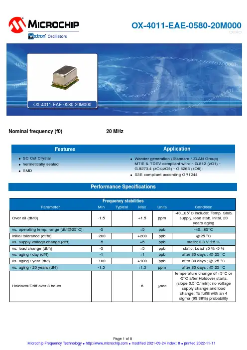
OX-4011-EAE-0580-20M000OCXONominal frequency (f0)20MHzFeaturesApplication•SC Cut Crystal •hermetically sealed •SMD•Wander generation (Standard /ZLAN Group)MTIE &TDEV compliant with:-G.812(zO1)-G.8273.4(zO4;zO5)-G.8263(zO6);•S3E compliant according GR1244Performance Specificationsall units in mmTP: max 260°C (@ solder joint, customer board level)T p: max: 10…30 secAdditional Information:This SMD oscillator has been designed for pick and place reflow solderingSMD oscillators must be on the top side of the PCB during the reflow process.Notes:Unless otherwise stated all values are valid after warm-up time and refer to typical conditions for supply voltage, frequency control voltage,load,temperature(25◦C).Subject to technical modification.USA:Europe:100Watts Street LandstrasseMt Holly Springs,P A1706574924NeckarbischofsheimGermanyTel:1.717.486.3411T el:+49(0)7268.801.0Fax:1.717.486.5920Fax:+49(0)7268.801.281Information contained in this publication regarding device applications and the like is provided only foryour convenience and may be superseded by updates.It is your reasonability to ensure that yourapplication meets with your specifications.MICROCHIP MAKES NO REPRESENT A TION ORWARRANTIES OF ANY KIND WHETHER EXPRESS OR IMPLIED,WRITTEN OR ORAL,ST ATUTORYOR OTHERWISE,RELA TED TO THE INFORMA TION INCLUDING,BUT NOT LIMITED TO ITSCONDITION,QUALITY,PERFORMANCE,MERCHANT ABILITY OR FITNESS FOR PURPOSE.Microchip disclaims all liability arising from this information and its e of Microchip devices in lifesupport and/or safety applications is entirely at the buyer’s risk,and the buyer agrees to defend,indemnify and hold harmless Microchip from any and all damages,claims,suits,or expenses resultingfrom such use.No licenses are conveyed,implicitly,or otherwise,under any Microchip intellectualproperty rights unless otherwise statedTrademarksThe Microchip and Vectron names and logos are registered trademarks of Microchip TechnologyIncorporated in the U.S.A.and other countries.List of appendicesAppendix_OX-4011-EAE-0580-20M000_Jitter II Appendix_OX-4011-EAE-0580-20M000_OX-401-9016-III 20M000_OX-4011-EAE-0580-10M000_MTIE_TDEVAppendix_OX-221-OX-40x_Power_on_time XIAppendix handling&processing note XIIThe following MTIE TDEV plots were generated from data collected on production devices over the course of a year and represent typical performance. Frequency is measured every second and converted to phase using Microchip’s golden standard TimeMonitor soft ware. Filtering is applied to the data per standards requirements, and limits where applicable, are shown in red. Additional information on standards and oscillatorrecommendations can be found in ZLAN-830 and ZLAN-3467 (formerly ZLAN-442 and ZLAN-68).Const. Temp ±1°K; slope 0,1°C/min, range 21..23°C Const. Temp ±5°F; slope 0,1°C/min,range 19.22..24.78°C Trapezoid_Pattern_slope 0,5°C/min,range +2,5...42,5°C Triangle-Pattern_slope 0,2°C/min,range -40...85°CConst. Temp ±1°K; slope 0,1°C/min, range 21..23°C Const. Temp ±5°F; slope 0,1°C/min,range 19.22..24.78°C Trapezoid_Pattern_slope 0,5°C/min,range +2,5...42,5°C Triangle-Pattern_slope 0,2°C/min,range -40...85°CConst. Temp ±1°K; slope 0,1°C/min, range 21..23°C Const. Temp ±5°F; slope 0,1°C/min,range 19.22..24.78°C Trapezoid_Pattern_slope 0,5°C/min,range +2,5...42,5°C Triangle-Pattern_slope 0,2°C/min,range -40...85°CConst. Temp ±1°K; slope 0,1°C/min, range 21..23°C Const. Temp ±5°F; slope 0,1°C/min,range 19.22..24.78°C Trapezoid_Pattern_slope 0,5°C/min,range +2,5...42,5°C Triangle-Pattern_slope 0,2°C/min,range -40...85°CConst. Temp ±1°K; slope 0,1, range 21..23°C Const. Temp ±5°F; slope 0,1,range 19.22..24.78°C Trapezoid_Pattern_slope 0,5,range +2,5...42,5°C Triangle-Pattern_slope 0,2,range -40...85°CConst. Temp ±1°K; slope 0,1, range 21..23°C Const. Temp ±5°F; slope 0,1,range 19.22..24.78°C Trapezoid_Pattern_slope 0,5,range +2,5...42,5°C Triangle-Pattern_slope 0,2,range -40...85°CConst. Temp ±1°K; slope 0,1, range 21..23°C Const. Temp ±5°F; slope 0,1,range 19.22..24.78°C Trapezoid_Pattern_slope 0,5,range +2,5...42,5°C Triangle-Pattern_slope 0,2,range -40...85°CConst. Temp ±1°K; slope 0,1, range 21..23°C Const. Temp ±5°F; slope 0,1,range 19.22..24.78°C Trapezoid_Pattern_slope 0,5,range +2,5...42,5°C Triangle-Pattern_slope 0,2,range -40...85°CApplicationUnless otherwise noted, the products listed in the catalogue are designed for use with ordinary electrical devices, such as stationary and portable communication, control, measurement equipment etc.. They are designed and manufactured to meet a high degree of reliability (lifetime more than 15 years) under normal …commercial“ application conditions. Products dedicated for automotive and H-Rel applications are specifically identified for these applications. If you intend to use these …commercial“ products for airborne, space or critical transport applications, nuclear power control, medical devices with a direct impact on human life, or other applications which require an exceptionally high degree of reliability or safety, please contact the manufacturer.Electrostatic SensitivityCrystal oscillators are electrostatic sensitive devices. Proper handling according to the established ESD handling rules as in IEC 61340-5-1 and EN 100015-1 is mandatory to avoid degradations of the oscillator performance due to damages of the internal circuitry by electrostatics. If not otherwise stated, our oscillators meet the requirements of the Human Body Model (HBM) according to JESD22-A114F.HandlingExcessive mechanical shocks during handling as well as manual and automatic assembly have to be avoided. If the oscillator was unintentionally dropped or otherwise subject to strong shocks, please verify that the electrical function is still within specification.Improper handling may also detoriate the coplanarity of bended leads of SMD components. SolderingOscillators can be processed using conventional soldering processes such as wave soldering, convection, infrared, and vapour phase reflow soldering under normal conditions. Solderability is guaranteed for one year storage under normal climatic conditions (+5°C to +35°C @ 40% to 75% relative humidity), however typically sufficient solderability –depending on the process – is maintained also for longer time periods. In cases of doubt, components older than one year should undergo a sample solderability test.The recommended reflow solder profile for SMT componets is according IPC/JEDEC J-STD-020 (latest revision)SMD oscillators must be on the top side of the PCB during the reflow process.After reflow soldering the frequency of the products may have shifted several ppm, which relaxes after several hours or days, depending on the products. For details please contact the manufacturer.CleaningCleaning is only allowed for hermetically sealed oscillators. Devices with non hermetical enclosures (e.g. with trimmer holes) shall not be cleaned by soaking or in vapour, because residues from the cleaning process may penetrate into the interior, and degrade the performance.Our products are laser marked. The marking of our oscillators is resistant to usual solvents, such as given in IEC 60068-2-45 Test XA. For applicable test conditions see IEC 60679-1.Ultrasonic cleaning is usually not harmful to oscillators at ultrasonic frequencies of 20kHz at the sound intensities conventional in industry. Sensitive devices may suffer mechanical damage if subjected to 40kHz ultrasound at high sound pressure. In cases of doubt, please conduct tests under practical conditions with the oscillators mounted on the PC board.Hermetical SealIf the device is specified as hermetically sealed, it meets the requirements of IEC 60679-1, i.e. for enclosures with a volume smaller than 4000mm³ the leak rate is below 5*10-8 bar cm3/s, for larger enclosures it is below 1*10-6 bar c bar cm3/s, tested according to IEC 60068-2-17 Test Qk.Glass feed-throughs may be damaged as a result of mechanical overload, such as bending the connection leads or cutting them with an unappropriated tool. In order to avoid microcracking, the wire must be held fixed in position by a pressure pad between glass feed-through and the bending point during the bending process. Check: there should be no damaged edges on the glass feed-through after the bending.Tape & ReelThe packing in tape and reel is according to IEC 60286-3.Details see tape & reel data sheets.QualificationVectron products are undergoing regular qualification/reliability tests as per product family definition. Results are available upon request. Customer specific qualification tests are subject to agreement.If not otherwise stated, the product qualifications are performed according to IEC 60679-5 or other valid industry standards.ScreeningOur oscillators are 100% tested, and all key manufacturing processes are controlled by Statistical Process Control (SPC). Additional screening is therefore usually not required.On request, we can perform screening tests according to MIL-PRF-55310, class B for discrete or hybrid constructions of commercial (COTS) products. For special requirements see the High Reliability Clock section.Demounting/Desoldering of Ocsillator device for analysis:The removal or desoldering of oscillators from customer application after SMT process may cause damage to the device if not handeld appropriately. It may lead to parametric change such as frequency shift (like OCXO: up to +/- 200 ppb) . It is utmost important to minimize the direct heat exposure to the device in order to avoid such effects. Use of hot air gun for desoldering should be avoided.A mechanical stress could also destroy the part, if exposed to excessive mechanical shock after removal process. Appropriate shock protection & ESD designated packaging must be used to avoid any external mechanical shock for FA return process.In general, the products* withstand the tests listed in the following Table 1, which are based on valid industry standards.*Additional note: Test conditions could vary for different product families and individual product specifications depending on the customer as well as product requirements.Recommended Environmental Test ConditionsTable 1。
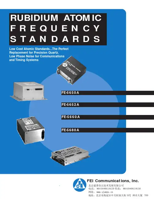
,FE-5680AFE-5660AFE-5652A FE-5650A 北京建普奇正技术发展有限公司电话:86+10+68118120 传真:86+10+68118130网址:www.ojumpo.cn地址:北京市海淀区中关村南大街31号 神舟大厦 709FE-5650AFE-5660A• STANDARD OUTPUT FREQUENCY IS 5OR 10 MHz• SHORT TERM:ALLAN DEVIATION 3x10-11/ t • LONG TERM: AGING 5x10-11/MONTH • TEMPERATURE: 3x10⁻¹⁰, -5 TO+50°CFE-5652A• EXTREMELY SMALL: 3x3x1.4 IN.• DIGITALLY PROGRAMMABLE TO 1x10-13• FREQUENCY: 1 Hz TO 20 MHz & 50.255+MHz• STABILITY OVER TEMPERATURE 3x10⁻¹⁰• STABILITY: 1.4x10⁻¹¹/ t , 2x1O -11/DAY2x10-9/YEARFE-5680A• EXTREMELY LOW SILHOUETTE:LESS THAN 1”• STABILITY OVER TEMPERATURE: 5x10-11• DIGITALLY PROGRAMMABLE TO 1x10-13• FREQUENCY: 1 Hz TO 20 MHz • FAST WARM UP:<5 MIN • STABILITY:TO 5x10-12/ tTO 2x10⁻¹⁰/YEAR• TEMPERATURE RANGE: -40°C to + 85°C • STABILITY OVER TEMPERATURE: 5x10-11• DIGITALLY PROGRAMMABLE TO 1x10-13• FREQUENCY: 1 Hz TO 20 MHz • FAST WARM UP:<5 MIN • STABILITY:TO 5x10-12/ t2x10-10/YEAR2TECHNICAL CHARACTERISTICSMODELFE-5650A FE-5652A FE-5660A FE-5680A POWER @25°C8W (Steady State)16W (Steady State)10W @24 VDC 11W (Steady State)32W(Peak)36W (Peak)-------------32W (Peak)WARM-UP TIME @25°C <4 min. to lock 5 min to lock <6 min. to 1x10⁻⁹<5 min. to lock POWER SUPPL Y 15-18V @500 mA 26 to 28 VDC 15V 15-18V @700 mA5V ±0.25 @100 mARIPPLE INPUT 15V @< 0.1 Vrms ---------------------------15V @< 0.1 Vrms OPERATING or 48 bit DDS or 48 bit DDS TEMPERATURE -5°C to +50°C -40 to +85°C -5° to +50°C -5°C to +50°C SIZE 1.44 x 3.03 x 3.00 2.97 x 6.0 x 6.3 2 x 3 x 40.98 x 3.4 x 4.9237 x 77 x 76 mm 75 X 178 x 160 mm 51 x 76 x 102 mm 25 x 88 x 125 mm 12 oz, 338 gms 3.06 Lbs, 1.388 Kgs 1.3 Lbs, 0.6 Kgs 15.3 oz, 434 gms SPECIFICATIONSFREQUENCY 10 MHz (Factory Settable 1 Hz to 20 MHz)OUTPUT0.5V rms into 50 ohm sinewave SETTABILITY 1 x 10-11(range 2 X 10⁻⁹)STABILITYALLAN DEVIATION 1.4 x 10⁻¹¹/t DRIFT 2 x 10⁻⁹/year 2 x 10-11/day RETRACE5 x 10-11INPUT VOLTAGESENSITIVITY2 X 10-11/15 to 16V SPURS60 dBc HARMONICS 30 dBc PHASE NOISE @10 Hz:-100 dBc (@10 MHz)@100 Hz:-125 dBc @1000 Hz:-145 dBc FREQUENCY VS TEMP .3 x 10-10 (-5 to +50°C)BITE Output, N O Fault/Fault L OGIC L EVEL Rb L OCK , 0/1 (TTL Compatible)Figure 13RUBIDIUM FREQUENCY STANDARDSFUNCTION DESCRIPTIONINPUT REGULATORSLOCK-IN AMPLIFIERRF GENERATOR SYNTHESIZER10 MHz OUTPUT FREQUENCY50.255+ MHz OUTPUTOUTPUT FREQUENCYBUFFER AMPLIFIER PROGRAMMABLE SYNTHESIZERRUBIDIUM PHYSICS PACKAGEEFCSERIAL DIGITINPUT+15VRTNINPUT VOLTAGE50.255+ MHz12345-OR--OR-EThe RFS uses the property of atomic resonance in a Rubidium Physics Package to control the output frequency of a 50.255+ MHz Voltage Controlled Crystal Oscillator (VCXO) via a Frequency Lock Loop (FLL). The FLL functional blocks consist of an RF Generator, Lock-in Amplifier and the Rubidium Physics Package. Frequency locking of the VCXO is accomplished by operating the Rubidium Physics Package as a frequency discriminator, i.e., departures of a frequency derived from an input signal (50.255+ MHz from the VCXO) from a defined center frequency (Rubidium atomic resonance) produce a DC output signal (control voltage). Once the FLL has been established, the system generates a loop-locked indication which can be monitored on pin 3. Depending on the option selected, the 50.255+ MHz VCXO output is used as the clock input for the DDS within the Synthesizer, the Digital Programmable Synthesizer or Buffer Amplifier.The Rubidium Physics Package utilizes the ground-state hyperfine transition of the Rubidium atom, at approximately 6.8+ GHz. In order to use this atomic transition, the Rubidium Physics Package incorporates a Rubidium cell, Rubidium lamp, and servo electronics. The VCXO is locked to the Rubidium atomic resonance at 6.8+ GHz. The VCXO frequency of 50.255+ MHz is an exact sub-multiple (x136) of the atomic resonance frequency at 6.8+ GHz.The error signal is generated in the physics package. Light from the Rubidium lamp, produced by an excited plasma discharge, is filtered and passed through the Rubidium resonance cell where it interacts with Rubidium atoms in the vapor. After passing through the resonance cell, this light is incident upon a photocell. When the applied microwave fre-quency is equal to 6.8+ GHz, the Rubidium atoms are resonated by the microwave field in the cavity; this causes the light reaching the photocell to decrease. The decrease in light, when the microwave frequency is equal to the sharply defined Rubidium frequency, is then converted electronically to an error signal with phase and amplitude information that is used to steer the VCXO via its control voltage and keep it on frequency at 50.255+ MHz.Output frequencies for Options 02 are provided by the Digital Programmable Synthesizer. Option 02 is an RS-232remote digitally controlled output with a frequency range of 2 x 10⁻⁷at a resolution of 5 x 10-12.Figure 24OPTIONSOPTION NO.FREQUENCY STABILITY284x10-12/day, 5x10⁻¹⁰/year 29 2x10⁻¹⁰/year after 1 year(4x10⁻¹⁰/month)31Allan Dev = 5x10-12/ t 32 f vs. T= ±1x10-1048 f vs. T= ±5x10-11OPTIONOUTPUT CHARACTERISTICS 02RS232 control*09Square Wave 12Analog Tuning16-80 dBc Spurious for ±5 MHz 21 1.0 V rms Output 26LOCK=TTL High30Analog Tuning: 0 to 10v 357E -9C-Fld Adj*Consult factoryOPTION INPUT VOLTAGE OPTIONS 2015 VDC2522 VDC to 32 VDC3415 & 5 VDC Input (FE-5660)46Reverse Voltage ProtectionOPTION OTHER18Conformally Coated22MIL environment (foamed)46Reverse Voltage ProtectionOPTION NO.OUTPUT FREQUENCY **0150.255055 MHz Sine Wave 03 5 MHz 0415 MHz 0513 MHz 06 2.048 MHz 0710.23 MHz***08Customer Frequency**Nominal Frequency ±5x10⁻⁸***1 Hz to 10 MHz sq. wave, TTL Comp., 5 MHz to 20 MHz sine wave.OPTION TEMPERATURE RANGE 36-44Consult Factory(from -55°c to +85°c)5Rubidium atomic frequency standards are beingused increasingly in telecommunication applications, particularly wireless telephone networks.The possibilityof frequency stability sufficient to eliminate the need for sched-uled re-calibrations, along with small size, low power require-ments, wide temperature range operation, and low cost, make these devices attractive candidates for telecommunication applications.In this paper, two new Rb frequency standard designs the FE5680A and FE5652A have been optimized for such appli-cations. The first design is a low profile device, in a package less than 1 inch in height. This device is designed to operate over the temperature range -10 to +60°C, with less than 1E-10 frequency error.The second design is a wide temperature range device, which operates from -40 to +85°C, with less than 1E-10 frequen-cy error. This unit employs a thermo-electric cooler to maintainthe Rb absorption elements at acceptable temperatures at the high end of the ambient temperature range.These devices are presently in production. Performance results of production devices are presented.IntroductionThe FE-5680A Rb frequency standard is 3.5 x 5 x 1 inches, a design suited to PC board slot mounted applications. This product is shown in Figure 1. A simplified functional block diagram is shown below. (Figure 3)The FE-5652A Rb frequency standard is 4.7 x 6 x 3 inches. This larger package allows space for a thermo-electric cooler for the physics package, as well as circuitry to lock the output fre-quency to a 1 PPS reference signal as provided by GPS receivers. This product is shown in Figure 3. A simplified block diagram is shown below.Many commercial applications for precision frequency standards demand performance over an extended tem-perature range. Often frequency variation with temperature is the performance-limiting feature of these devices for CDMA holdover applications. The two products described in this paper have both been designed to operate over extended temperature ranges while guaranteeing a frequency variation of less than1E-10. The FE-5680A operates at any temperature between -10 and +60°C, a temperature range required for indoor rack-mounted telecommunication hardware with limited air flow. The FE-5652A operates at any temperature between -40 and+85°C, a temperature range required for outdoor, limited access, low maintenance telecommunication hardware.General Performance CharacteristicsPerformance characteristics for these Rb frequency standards are shown in electrical characteristics and options.It is immediately apparent the performance of the two designs is very similar. The only differences are that the FE-5652A requires a 28 VDC (nominal) input, and whereas the FE-5680A requires a 15 VDC (nominal) input. The power dissipation of the FE-5652A is 16 watts, as opposed to the 11 watts dissipated by the FE-5680A. The extra power required for the FE-5652A is needed for the thermo-electric circuit and the external reference lock circuitry.Frequency vs. TemperatureAs mentioned above, frequency variations due to ambi-ent temperature variations can easily swamp other sources of instability for a Rb frequency standard operating in a real life environment. Therefore special attention was given to frequency stability vs. temperature in these designs. Figures 5 and 6 show typical performance data for FE-5680A and FE-5652A Rb stan-dards over the ambient temperature range. In addition to the information provided by these plots, it is useful to understand the distribution of performance associated with a production lot of these devices. Table 2 provides this information.Figure3Figure4Block Diagram, FE-5652A6Table 2Frequency vs. Temperature Statistics, FE-5680ALot ID No. of Units Mean ∆f Std. Dev.(E-10)(E-10)43340.000.3044436-0.090.416The information in this table shows that the mean total frequency deviation over temperature is very small. What this really means is that the frequency deviation is equally likely to be positive or negative. The standard deviation values give an indication of the range of deviations to be expected amongst production devices.Frequency StabilityAllan deviation stability data for the FE5680A and FE5652A Rb standards are shown in Figure 7. The measurements used to derive the Allan deviation were all made at 25°C. It is of interest to note that the result for SN 4005 is significantly improved by comparing it to another Rb standard (SN 5339) rather than a Cs reference. This indicates that the result is limited by the stability of the Cs reference.Figure 7Allan Variance for several unitsSummaryPerformance results for two new Rubidium frequency standard products have been reported. These products continue thetrend toward small, robust, high-performance atomic frequency standards capable of operating in harsh non-laboratory environ-ments, yet providing stabilities approaching those measured under controlled laboratory conditions. These devices are well suited to the demands of the telecommunications industry for increasingly precise time and frequency references capable of operating un-attended in harsh environments.7FOR CONSTANT FREQUENCY OFFSET 8FOR LINER FREQUENCY DRIFT95650A5652A 10TABLE 1PIN FUNCTION1+15V2+15V RTN3LOCK INDICATOR (BIT)4+5V5+5V RTN6NC7FINE TUNE RTN8FINE TUNE9NCPART NUMBER OF THIS DEVICE IS CONTROLLED BY CCD B115010-134805680A5660A11PINTABLE123456789FUNCTION +15V GND RB LOCK/UNLOCK N/C GND N/C FACTORY USE ONLY ANALOG TUNING N/COTHER FEI PRODUCTS FE-102A - CRYSTAL OSCILLATOROPERATION @100 MHzWITH LOW PHASENOISE: -172 dBcFE-101A - CRYSTAL OSCILLATORSUBMINIATURE OVEN CONTROLLED DESIGN,ONLY 1.27"X1.33"X1.33"WITH FAST WARM UP –LESS THAN 2 MINUTES FE-103A - CRYSTAL OSCILLATORDOUBLE OVEN DESIGNWITH EXCELLENT STABILITY:1X10-11/SECFE-7923A - DISTRIBUTION AMPLIFIERAN ECONOMICAL, 10-CHANNEL SINEWAVEDISTRIBUTION AMPLIFIEROPERATING FROM 1 MHzTHROUGH 10 MHz北京建普奇正技术发展有限公司电话:86+10+68118120 传真:86+10+68118130网址:www.ojumpo.cn地址:北京市海淀区中关村南大街31号神舟大厦709室。
铁硅铝磁环电感
铁硅铝磁环电感是一种被广泛使用的电感元件。
它主要由形状为
圆环的硅钢片、铝箔片及螺纹组成,是目前市场上最常用的电感元件
之一。
有时也称为晶振线圈、现代晶振环以及现代晶体线圈。
铁硅铝
磁环电感具有高效率、体积小、重量轻、易于安装和控制的优势。
此外,铁硅铝磁环电感的优势还在于能够实现高精度、高稳定性
及高灵敏度的测量,可以实现低压驱动和高压驱动,使用寿命长,耐
高温性好,能够承受大的电流而不受影响,可减少测量误差,可以实
现低噪声环境。
另外,铁硅铝磁环电感的纹波抑制能力差,容易受歪曲干扰影响,其频宽有限,电容和电阻效应不佳,生产成本高,维护难度大,受温
度变化影响大,功耗低,但性能不稳定。
同时,这种电感元件的工作
温度范围有限,一般以-20℃~125℃为宜,高温下可能会造成磁路损坏,导致电感变形。
总之,铁硅铝磁环电感是目前市场上最常用的电感元件之一,具
有高效率、体积小、重量轻、稳定性高、灵敏度高等优点,但也存在
着一些缺点,例如纹波抑制能力差、频宽有限、电容和电阻效应不佳、受温度变化影响大等。
因此,在购买铁硅铝磁环电感时,应考虑到其
优缺点,选择合适的规格及用途,以便得到最佳的应用效果。
vn5650用法-回复*以下文章仅为示例,实际用法可能因产品实际情况存在差异,请以产品说明书为准。
*vn5650用法介绍vn5650是一款功能强大的设备,适用于各种电子设备和电路板的测试和诊断。
它具有多种功能和使用场景,如信号发生器、频谱分析仪、网络分析仪等。
在本文中,我们将逐步介绍vn5650的使用方法,帮助您充分了解和掌握这款设备。
第一步:了解vn5650的基本功能vn5650是一款集成了多种仪器的多合一测试设备。
它可以作为信号发生器,输出各种波形信号,如正弦波、方波、三角波等。
同时,它还具备频谱分析仪的功能,可以分析信号的频谱特性。
此外,vn5650还可作为网络分析仪,检测电路板的网络参数,如阻抗、传输函数等。
因此,vn5650非常适合电子设备的测试和诊断工作。
第二步:连接vn5650到电子设备在开始使用vn5650之前,需要将其连接到待测试的电子设备上。
首先,将vn5650的电源线连接到电源插座,并打开电源开关。
然后,使用合适的连接线(如BNC线)将vn5650的输出端口与待测试设备的输入端口连接。
确保连接牢固可靠,以免出现松动或接触不良的情况。
第三步:选择需要测试的功能模式一旦vn5650与待测试设备连接好,可以通过触摸屏或旋钮选择需要测试的功能模式。
vn5650提供了直观的操作界面,用户可以通过触摸屏选择不同的测试模式,也可以通过旋钮进行调整和设置。
根据具体的测试需求,选择相应的功能模式,例如信号发生器模式、频谱分析仪模式或网络分析仪模式。
第四步:设置测试参数和启动测试在选定功能模式之后,需要设置测试参数以及启动测试。
对于信号发生器模式,可以设置信号频率、幅度和波形类型等参数,并启动信号输出。
对于频谱分析仪模式,可以设置频谱范围、分辨率和显示方式等参数,并启动频谱分析。
对于网络分析仪模式,可以设置测试频率和扫描速度等参数,并启动网络分析。
根据具体的测试需求,设置好参数后,点击启动按钮开始测试。

铁硅铝磁环型号-概述说明以及解释1.引言1.1 概述概述铁硅铝磁环是一种常见的磁性材料,它由铁、硅和铝等元素组成。
铁硅铝磁环具有良好的磁性能和热稳定性,广泛应用于电力电子、通信、汽车、家电等领域。
本文将介绍铁硅铝磁环的基本概念和原理,探讨其在各个应用领域中的具体应用,并总结铁硅铝磁环的特点和优势。
此外,我们还将展望铁硅铝磁环的发展前景,分析其在未来的研究和应用中可能面临的挑战和机遇。
通过深入了解铁硅铝磁环的特性和应用,我们可以更好地理解和利用这种磁性材料,推动其在各个领域中的发展和创新。
接下来,我们将逐步展开铁硅铝磁环相关内容的阐述,以期为读者提供有益的参考和启示。
1.2 文章结构本文将分为引言、正文和结论三个部分来介绍铁硅铝磁环型号。
具体结构如下:1) 引言部分将对铁硅铝磁环的概述进行介绍,包括它的基本概念、应用领域以及本文的目的。
2) 正文部分将更详细地阐述铁硅铝磁环的基本概念和原理,包括其组成成分、制作工艺和磁性能等方面的内容。
同时,该部分还将探讨铁硅铝磁环在不同领域的应用情况,例如电力电子、电机和传感器等。
通过对其特点和应用领域的介绍,读者可以更好地了解铁硅铝磁环的作用和优势。
3) 结论部分将对铁硅铝磁环的特点和优势进行总结,并展望其未来的发展前景。
通过分析目前的研究进展和市场需求,可以提供对铁硅铝磁环在各个领域中的应用前景进行合理的预测。
通过以上的文章结构,读者可以系统地了解铁硅铝磁环型号的相关知识,并从不同角度进行深入的探讨和思考。
这将帮助读者更好地理解铁硅铝磁环的特点和应用,为相关研究和应用提供参考依据。
1.3 目的文章目的部分的内容可以围绕以下内容进行撰写:文章的目的是为了全面介绍铁硅铝磁环的型号,包括其基本概念、原理、应用领域以及其特点和优势。
通过深入了解铁硅铝磁环的性能和特点,读者可以更好地了解这种材料的用途和优点,进而为相关行业的技术研发、产品设计和制造提供参考和指导。
具体地说,本文的目的可以从以下几个方面来阐述:1. 增加读者对铁硅铝磁环的了解。
大功率铁硅铝磁环电感
铁硅铝磁环电感是一种电子元件,它是由铁、硅和铝的磁性材料制成的环状结构,内部绕有导线。
由于这种电感具有高电感性能和优异的高频性能,因此被广泛应用于高频电子电路、通讯设备、医疗设备等领域。
铁硅铝磁环电感的核心材料是铁硅铝磁性材料,在加工制作过程中,其薄片经过精心的设计和组装,形成了一个环状结构。
金属导线穿过环的中心,形成了一个线圈。
当电流进入线圈时,会在铁硅铝磁性材料中形成一个磁场。
这个磁场将储存电荷并产生电感性能。
铁硅铝磁环电感具有很高的电感和低的损耗,对于高频信号的传输和滤波作用非常显著。
此外,铁硅铝磁环电感的额定电流和负载容量较大,可以同时承载多个电源,提高了电子电路的稳定性和稳定性。
铁硅铝磁环电感主要应用于高频电子电路,例如无线传输、RFID技术、通讯设备等。
在这些应用中,电感器的频率是很高的,在高频条件下,铁硅铝磁环电感不仅可以维持高电感性能,还能够有效的抑制干扰信号,减小电路的电磁辐射和噪声等问题。
除了在高频电子电路中的应用外,铁硅铝磁环电感还可以被应用于一些精密设备,例如医疗电子设备和汽车电子设备。
此类设备要求精度高、敏感度高,而铁硅铝磁环电感正好可以提供这样的特性。
总的来说,铁硅铝磁环电感是一种高性能电子元器件。
它的优异性能和多样化的应用使其成为了许多高技术领域中必不可少的重要组成部分。
cr型张弛振荡器电阻-电容-概述说明以及解释1. 引言1.1 概述CR型张弛振荡器是一种常见的电路结构,它由一个电容器和一个电阻器组成。
在电路中,电容器会逐渐充电或放电,而电阻器起到控制电容器充放电速率的作用。
通过调节电阻器的阻值,我们可以控制振荡器的频率。
本文将着重介绍CR型张弛振荡器的原理及其在实际应用中的作用。
在正文部分,我们将详细讨论电阻和电容对振荡器工作的影响,以及振荡器的工作原理。
通过阐述这些内容,我们希望读者对CR型张弛振荡器有一个更深入的了解。
本文的目的是使读者了解CR型张弛振荡器的基本原理,以及电阻和电容在该电路中的重要作用。
我们将讨论振荡器的工作方式,并探讨一些相关的应用领域。
最后,我们将总结文章并对CR型张弛振荡器的未来发展进行展望。
在展望部分,我们将探讨该振荡器的潜在改进和扩展应用,以及可能遇到的挑战。
我们希望通过这篇文章,读者能够对CR型张弛振荡器有一个全面的了解,并对其在电路设计和相关领域中的应用有一定的启发。
总之,本文将介绍CR型张弛振荡器的原理和作用,并对其未来发展进行展望。
通过阅读本文,读者将对该振荡器的工作原理有一个更深入的了解,并能够在实际应用中灵活运用。
希望本文能为读者提供有价值的信息和启示。
文章结构部分的内容如下:1.2 文章结构本篇长文主要介绍了CR型张弛振荡器以及电阻-电容在其中的作用。
文章按照以下内容结构进行展开:第一部分是引言,其中包括对整篇文章的概述,简要介绍了CR型张弛振荡器的背景和基本概念,阐明了本文的研究意义和目的。
第二部分为正文,主要分为三个小节。
首先介绍了CR型张弛振荡器的基本原理和结构,包括其中的电路组成和工作原理,以及常见的电阻-电容的配置方式。
接着,详细探讨了电阻-电容在CR型张弛振荡器中的作用。
通过分析电阻和电容在电路中的相互作用,解释了它们对振荡器性能的影响,以及通过调节电阻和电容参数来实现振荡频率的调整等。
最后,阐述了振荡器的工作原理,包括振荡器中电阻-电容的充放电过程和信号放大机制等。
106125铁硅铝磁环参数摘要:1.铁硅铝磁环的概述2.106125 铁硅铝磁环的主要参数3.106125 铁硅铝磁环的应用领域4.106125 铁硅铝磁环的优势和特点正文:一、铁硅铝磁环的概述铁硅铝磁环,又称铁硅铝氧磁环,是一种具有良好磁性能和电性能的金属软磁材料。
它是由铁、硅、铝和氧四种元素组成的复合材料,通过一定的工艺制成环状,具有很高的磁导率和磁感应强度。
铁硅铝磁环广泛应用于电子元器件、磁性材料、磁悬浮列车、磁共振成像等领域。
二、106125 铁硅铝磁环的主要参数106125 铁硅铝磁环的具体参数可能因生产厂家和应用领域而有所不同。
一般来说,这类磁环的主要参数包括磁导率、磁感应强度、矫顽力、居里温度等。
其中,磁导率是衡量磁环磁性能的重要指标,它反映了磁环对磁场的响应能力;磁感应强度则表示磁环产生的磁场强度;矫顽力是磁环抵抗外加磁场作用的能力;居里温度则是磁环磁性能发生突变的温度。
三、106125 铁硅铝磁环的应用领域106125 铁硅铝磁环作为一种高性能的软磁材料,在许多领域都有广泛应用。
以下是一些典型的应用领域:1.电子元器件:铁硅铝磁环可用于制作电感器、变压器、磁性传感器等电子元器件,具有很高的工作效率和稳定性。
2.磁性材料:铁硅铝磁环可用于制造磁性材料,如磁卡、磁带、磁扣等,具有较好的抗干扰性能和数据存储能力。
3.磁悬浮列车:铁硅铝磁环在磁悬浮列车的磁浮系统中有重要应用,可提高列车的运行速度和稳定性。
4.磁共振成像:铁硅铝磁环在磁共振成像设备中有广泛应用,有助于提高成像的清晰度和准确性。
四、106125 铁硅铝磁环的优势和特点106125 铁硅铝磁环具有以下优势和特点:1.高磁导率:铁硅铝磁环具有较高的磁导率,能够有效提高电子元器件的工作效率。
2.良好的抗干扰性能:铁硅铝磁环具有较好的抗干扰性能,可提高磁性材料的数据存储稳定性。
3.宽温域应用:铁硅铝磁环具有较宽的温域范围,可在不同温度环境下保持良好的磁性能。
铁粉磁环铁硅铝电感
铁粉磁环,作为一种常见的电感元件,广泛应用于各种电子设备中。
它由铁、硅和铝等材料组成,具有优异的磁性能和导电性能。
铁粉磁环的制作过程相对简单,首先需要将铁、硅和铝等材料按照一定比例混合均匀,然后通过压制和烧结等工艺形成磁环的形状。
磁环的内外表面都经过精细的处理,以提高其磁场的稳定性和传导效率。
铁粉磁环的主要作用是产生和调节电磁场。
在电子设备中,它常用于电感器、变压器和滤波器等电路中,起到存储和传输电能的作用。
当电流通过铁粉磁环时,由于其磁性特性,会产生一个稳定的磁场,进而影响周围的电路。
铁粉磁环的特点之一是可调性。
通过改变磁环的材料组成、形状和尺寸等参数,可以调节磁场的强弱和频率响应。
这使得铁粉磁环在不同的电子设备中具有广泛的应用,能够满足不同的电路需求。
除了在电子设备中的应用,铁粉磁环还常用于电动机和发电机等电动机械设备中。
在这些设备中,它可以增加磁场的强度和稳定性,提高电机的效率和性能。
铁粉磁环作为一种重要的电感元件,在现代电子技术和电动机械领域中发挥着重要作用。
它的材料组成和制作工艺决定了其优异的磁性能和导电性能。
通过合理调节磁环的参数,可以满足不同电路和
设备的要求。
铁粉磁环的应用范围广泛,为电子科技的发展做出了重要贡献。
vn5650用法-回复VN5650是一种非常有用的设备,它在许多领域中发挥着重要作用。
本文将一步一步回答VN5650的用法,并探讨其在不同领域中的应用。
第一步:了解VN5650的基本知识首先,我们需要了解VN5650是什么以及它的基本特征。
VN5650是一种多功能万用表,具有测量电压、电流、电阻、电容、电感等参数的能力。
它还具有数据记录和自动测量功能,适用于各种实验室和工业环境。
VN5650的特点之一是其高精度和可靠性,因此它被广泛应用于测试、维修和工程领域。
第二步:使用VN5650进行基本测量现在我们已经了解了VN5650的基本特征,接下来是学习如何使用它进行基本测量。
首先,我们需要准备一个合适的测量电路,并将VN5650连接到电源。
然后,我们可以选择测量参数并设置测量范围。
VN5650将根据我们的设置显示测量结果,并提供准确的测量值。
根据需要,我们还可以选择数据记录功能,以便后续分析。
第三步:VN5650在电子工程领域中的应用现在我们已经了解了如何使用VN5650进行基本测量,接下来是探讨它在电子工程领域中的应用。
作为一个万用表,VN5650可以帮助工程师进行各种参数的测量,例如电压、电流和电阻。
这对于设计、调试和维修电子电路非常重要。
此外,VN5650还具有快速测量功能,可以提高工作效率。
因此,它被广泛应用于电子工程实验室和制造业。
第四步:VN5650在实验室研究中的应用除了电子工程领域,VN5650还被广泛应用于科学实验室中。
它可以帮助研究人员进行各种实验参数的测量,例如电容、电感和电阻等。
这些测量结果对于研究和分析电路性能非常重要。
此外,VN5650具有自动测量功能,可以快速准确地记录数据。
这对于长期实验和大规模数据采集非常有用。
第五步:VN5650在工业维修中的应用最后,VN5650还在工业维修领域中发挥着重要作用。
维修人员可以使用VN5650测量和识别故障电路的问题,并根据测量结果进行修理。
FE-5650A 铷原子振荡器产品概述FE-5650A是铷原子振荡器是美国 FEI 公司生产的高性能铷原子振荡器产品,其准确度高,价格低廉,被广泛应用于电信、时统、计量标准等领域。
西安同步电子科技有限公司有售产品功能1)提供一路标准的10MHz正弦信号;2)RS-232管理控制接口。
产品特点a)尺寸小,体积轻;b)频率稳定度高;c)预热时间短;d)输出频率可选。
典型应用1)电信、时统、计量标准;2)通信系统频率标准;3)高稳晶振的更新换代产品。
技术指标射频输出频率10MHz电平正弦幅度0.5V rms 负载50Ω路数1路串行通信接口协议RS232电源输入功耗<8瓦(稳态) @ 25 ℃32瓦峰值输入电压15~18VDC(500mA)5V+0.25V (100mA)电源纹波15V:<0.1Vrms5V<0.020Vrms物理尺寸尺寸37×77×76mm 重量<338g MTBF >10万小时电气特性工作温度-5℃~+50℃频率变化(全温度范围)±3E- 10(-5℃~+50℃)频率变化(全电压范围)<2E- 11性能参数短稳≤1.4E-11/1s≤4.4E-12/10s≤1.4E-12/100s相噪≤-100dBc/Hz(10Hz)≤-125dBc/Hz(100Hz)≤-145dBc/Hz(1KHz) 谐波≤-30dBc杂波≤-60dBc准确度(出厂设置)±5E-11重现性±5E-11老化率2E- 9 /年2E- 11 /天数字调节频率范围2E- 7最小步进 1.74E- 14模拟调节范围2E- 7(“C”电位器)2E- 9(0到 5V电压)最小步进1E-11输入电压0 ~5V预热时间4分钟安装尺寸:。
FE-5650A 铷原子振荡器
产品概述
FE-5650A是铷原子振荡器是美国 FEI 公司生产的高性能铷原子振荡器产品,其准确度高,价格低廉,被广泛应用于电信、时统、计量标准等领域。
西安同步电子科技有限公司有售
产品功能
1)提供一路标准的10MHz正弦信号;
2)RS-232管理控制接口。
产品特点
a)尺寸小,体积轻;
b)频率稳定度高;
c)预热时间短;
d)输出频率可选。
典型应用
1)电信、时统、计量标准;
2)通信系统频率标准;
3)高稳晶振的更新换代产品。
技术指标
射频输出频率10MHz
电平正弦
幅度0.5V rms 负载50Ω
路数1路
串行通信接口协议RS232
电源输入功耗
<8瓦(稳态) @ 25 ℃
32瓦峰值
输入电压
15~18VDC(500mA)
5V+0.25V (100mA)
电源纹波
15V:<0.1Vrms
5V<0.020Vrms
物理尺寸尺寸37×77×76mm 重量<338g MTBF >10万小时
电气特性工作温度-5℃~+50℃
频率变化(全温度范围)±3E- 10(-5℃~+50℃)频率变化(全电压范围)<2E- 11
性能参数短稳
≤1.4E-11/1s
≤4.4E-12/10s
≤1.4E-12/100s
相噪
≤-100dBc/Hz(10Hz)
≤-125dBc/Hz(100Hz)
≤-145dBc/Hz(1KHz) 谐波≤-30dBc
杂波≤-60dBc
准确度(出厂设置)±5E-11
重现性±5E-11
老化率
2E- 9 /年
2E- 11 /天
数字调节频率范围2E- 7
最小步进 1.74E- 14
模拟调节范围
2E- 7(“C”电位器)
2E- 9(0到 5V电压)最小步进1E-11
输入电压0 ~5V
预热时间4分钟安装尺寸:。