基于XC164CS微处理器的正弦脉宽调制信号的实现
- 格式:pdf
- 大小:118.85 KB
- 文档页数:3

实验报告课程名称:电机控制指导老师:成绩:实验名称:正弦脉宽调制变频调速系统实验类型:同组学生姓名:一、实验目的和要求(必填) 二、实验内容和原理(必填) 三、主要仪器设备(必填) 四、操作方法和实验步骤 五、实验数据记录和处理六、实验结果与分析(必填)七、讨论、心得一、实验目的1、加深理解自然采样法生成SPWM 波的机理和过程。
2、熟悉SPWM 变频调速系统中直流回路、逆变桥功率器件和微机控制电路之间的连 接。
3、了解SPWM 变频器运行参数和特性。
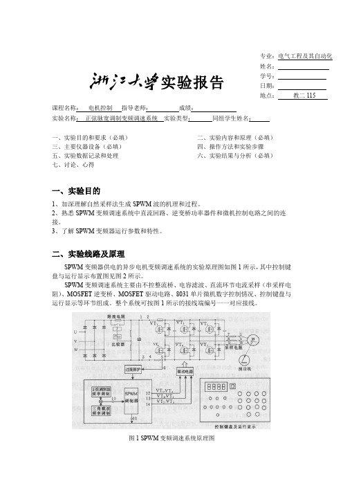
二、实验线路及原理SPWM 变频器供电的异步电机变频调速系统的实验原理图如图1所示,其中控制键盘与运行显示布置图见图2所示。
SPWM 变频调速系统主要由不控整流桥、电容滤波、直流环节电流采样(串采样电阻)、MOSFET 逆变桥、MOSFET 驱动电路、8031单片微机数字控制情况、控制键盘与运行显示等环节组成。
整个系统可按图1所示的接线端编号一一对应接线。
图1 SPWM 变频调速系统原理图本实验系统的性能指标如下:(1)运行频率f1可在1~60Hz的范围内连续可调。
(2)调制方式1)同步调制:调制比F r=3~123可变,步增量为3;2)异步调制:载波频率f0=0.5~8kHz可变,步增量为0.5kHz;3)混合调制:系统自动确定各运行频率下的调制比。
图2 SPWM变频器控制键盘与运行显示面板图(3)V/f曲线有四条V/f曲线可供选择,以满足不同的低频电压补偿要求,如图3所示。
曲线1: f1=1~50Hz, U1/f1=220/50=4.4V/Hzf1=51~60Hz,U1=220V曲线2:f1=1~5Hz, U1=21.5Vf1=6~50Hz,U1/f1=220/50=4.4V/Hzf1=51~60Hz, U1=220V曲线3:f1=1~8Hz, U1=34.5Vf1=9~50Hz,U1/f1=220/50=4.4V/Hzf1=51~60Hz, U1=220V曲线4:f1=1~10Hz, U1=43Vf1=11~50Hz,U1/f1=220/50=4.4V/Hzf1=51~60Hz, U1=220V(4)加速时间可在1~60s区间设定电机从静止加速到额定速度所需时间,10s以下步增量为1s,10s到60s步增量为5s。
Data Sheet, V2.2, March 2006MicrocontrollersXC164CS-16F16-Bit Single-Chip Microcontroller with C166SV2 Core元器件交易网元器件交易网Edition 2006-03Published byInfineon Technologies AG81726 München, Germany© Infineon Technologies AG 2006.All Rights Reserved.Legal DisclaimerThe information given in this document shall in no event be regarded as a guarantee of conditions orcharacteristics (“Beschaffenheitsgarantie”). With respect to any examples or hints given herein, any typical values stated herein and/or any information regarding the application of the device, Infineon Technologies herebydisclaims any and all warranties and liabilities of any kind, including without limitation warranties of non-infringement of intellectual property rights of any third party.InformationFor further information on technology, delivery terms and conditions and prices please contact your nearestInfineon Technologies Office ().WarningsDue to technical requirements components may contain dangerous substances. For information on the types in question please contact your nearest Infineon Technologies Office.Infineon Technologies Components may only be used in life-support devices or systems with the express written approval of Infineon Technologies, if a failure of such components can reasonably be expected to cause the failure of that life-support device or system, or to affect the safety or effectiveness of that device or system. Life support devices or systems are intended to be implanted in the human body, or to support and/or maintain and sustain and/or protect human life. If they fail, it is reasonable to assume that the health of the user or other persons may be endangered.Data Sheet, V2.2, March 2006MicrocontrollersXC164CS-16F16-Bit Single-Chip Microcontroller with C166SV2 Core元器件交易网XC164Revision History: V2.2, 2006-03Previous Version(s):V2.1, 2003-06V2.0, 2003-01V1.0, 2002-03Page Subjects (major changes since last revision)all Layout of graphics and text structures has been adapted to the new company documentation rules.55Footnote about leakage current at P3.15 added.67Minimum oscillator period corrected71Output delay/hold time of A23 … A16 moved from tc11->tc12, tc21->tc23 74Chapter “Package and Reliability” added.We Listen to Your CommentsAny information within this document that you feel is wrong, unclear or missing at all? Your feedback will help us to continuously improve the quality of this document. Please send your proposal (including a reference to this document) to:ments@Table of Contents Table of Contents1Summary of Features . . . . . . . . . . . . . . . . . . . . . . . . . . . . . . . . . . . . . . . . 42General Device Information . . . . . . . . . . . . . . . . . . . . . . . . . . . . . . . . . . . 7 2.1Introduction . . . . . . . . . . . . . . . . . . . . . . . . . . . . . . . . . . . . . . . . . . . . . . . . . 7 2.2Pin Configuration and Definition . . . . . . . . . . . . . . . . . . . . . . . . . . . . . . . . . 83Functional Description . . . . . . . . . . . . . . . . . . . . . . . . . . . . . . . . . . . . . . 17 3.1Memory Subsystem and Organization . . . . . . . . . . . . . . . . . . . . . . . . . . . . 18 3.2External Bus Controller . . . . . . . . . . . . . . . . . . . . . . . . . . . . . . . . . . . . . . . 20 3.3Central Processing Unit (CPU) . . . . . . . . . . . . . . . . . . . . . . . . . . . . . . . . . 21 3.4Interrupt System . . . . . . . . . . . . . . . . . . . . . . . . . . . . . . . . . . . . . . . . . . . . 23 3.5On-Chip Debug Support (OCDS) . . . . . . . . . . . . . . . . . . . . . . . . . . . . . . . 28 3.6Capture/Compare Units (CAPCOM1/2) . . . . . . . . . . . . . . . . . . . . . . . . . . . 29 3.7The Capture/Compare Unit CAPCOM6 . . . . . . . . . . . . . . . . . . . . . . . . . . . 32 3.8General Purpose Timer (GPT12E) Unit . . . . . . . . . . . . . . . . . . . . . . . . . . . 33 3.9Real Time Clock . . . . . . . . . . . . . . . . . . . . . . . . . . . . . . . . . . . . . . . . . . . . 37 3.10A/D Converter . . . . . . . . . . . . . . . . . . . . . . . . . . . . . . . . . . . . . . . . . . . . . . 39 3.11Asynchronous/Synchronous Serial Interfaces (ASC0/ASC1) . . . . . . . . . . 40 3.12High Speed Synchronous Serial Channels (SSC0/SSC1) . . . . . . . . . . . . 41 3.13TwinCAN Module . . . . . . . . . . . . . . . . . . . . . . . . . . . . . . . . . . . . . . . . . . . . 42 3.14Watchdog Timer . . . . . . . . . . . . . . . . . . . . . . . . . . . . . . . . . . . . . . . . . . . . 44 3.15Clock Generation . . . . . . . . . . . . . . . . . . . . . . . . . . . . . . . . . . . . . . . . . . . . 45 3.16Parallel Ports . . . . . . . . . . . . . . . . . . . . . . . . . . . . . . . . . . . . . . . . . . . . . . . 45 3.17Power Management . . . . . . . . . . . . . . . . . . . . . . . . . . . . . . . . . . . . . . . . . . 47 3.18Instruction Set Summary . . . . . . . . . . . . . . . . . . . . . . . . . . . . . . . . . . . . . . 48 4Electrical Parameters . . . . . . . . . . . . . . . . . . . . . . . . . . . . . . . . . . . . . . . 51 4.1General Parameters . . . . . . . . . . . . . . . . . . . . . . . . . . . . . . . . . . . . . . . . . 51 4.2DC Parameters . . . . . . . . . . . . . . . . . . . . . . . . . . . . . . . . . . . . . . . . . . . . . 54 4.3Analog/Digital Converter Parameters . . . . . . . . . . . . . . . . . . . . . . . . . . . . 59 4.4AC Parameters . . . . . . . . . . . . . . . . . . . . . . . . . . . . . . . . . . . . . . . . . . . . . 62 4.4.1Definition of Internal Timing . . . . . . . . . . . . . . . . . . . . . . . . . . . . . . . . . . 62 4.4.2On-chip Flash Operation . . . . . . . . . . . . . . . . . . . . . . . . . . . . . . . . . . . . 66 4.4.3External Clock Drive XTAL1 . . . . . . . . . . . . . . . . . . . . . . . . . . . . . . . . . 67 4.4.4Testing Waveforms . . . . . . . . . . . . . . . . . . . . . . . . . . . . . . . . . . . . . . . . 68 4.4.5External Bus Timing . . . . . . . . . . . . . . . . . . . . . . . . . . . . . . . . . . . . . . . . 69 5Package and Reliability . . . . . . . . . . . . . . . . . . . . . . . . . . . . . . . . . . . . . . 74 5.1Packaging . . . . . . . . . . . . . . . . . . . . . . . . . . . . . . . . . . . . . . . . . . . . . . . . . 74 5.2Flash Memory Parameters . . . . . . . . . . . . . . . . . . . . . . . . . . . . . . . . . . . . 75XC164 16-Bit Single-Chip Microcontroller with C166SV2 CoreXC166Family1Summary of Features•High Performance 16-bit CPU with 5-Stage Pipeline–25 ns Instruction Cycle Time at 40 MHz CPU Clock (Single-Cycle Execution)–1-Cycle Multiplication (16 × 16 bit), Background Division (32 / 16 bit) in 21 Cycles –1-Cycle Multiply-and-Accumulate (MAC) Instructions–Enhanced Boolean Bit Manipulation Facilities–Zero-Cycle Jump Execution–Additional Instructions to Support HLL and Operating Systems–Register-Based Design with Multiple Variable Register Banks–Fast Context Switching Support with Two Additional Local Register Banks–16 Mbytes Total Linear Address Space for Code and Data–1024 Bytes On-Chip Special Function Register Area (C166 Family Compatible)•16-Priority-Level Interrupt System with up to 75 Sources, Sample-Rate down to 50 ns •8-Channel Interrupt-Driven Single-Cycle Data Transfer Facilities via Peripheral Event Controller (PEC), 24-Bit Pointers Cover Total Address Space •Clock Generation via on-chip PLL (factors 1:0.15 … 1:10), orvia Prescaler (factors 1:1 … 60:1)•On-Chip Memory Modules– 2 Kbytes On-Chip Dual-Port RAM (DPRAM)–2/4 Kbytes On-Chip Data SRAM (DSRAM)1)– 2 Kbytes On-Chip Program/Data SRAM (PSRAM)–64/128 Kbytes On-Chip Program Memory (Flash Memory or Mask ROM)1)•On-Chip Peripheral Modules–14-Channel A/D Converter with Programmable Resolution (10-bit or 8-bit) and Conversion Time (down to 2.55 µs or 2.15 µs)–Two 16-Channel General Purpose Capture/Compare Units (12 Input/Output Pins)–Capture/Compare Unit for flexible PWM Signal Generation (CAPCOM6) (3/6 Capture/Compare Channels and 1 Compare Channel)–Multi-Functional General Purpose Timer Unit with 5 Timers–Two Synchronous/Asynchronous Serial Channels (USARTs)–Two High-Speed-Synchronous Serial Channels–On-Chip TwinCAN Interface (Rev. 2.0B active) with 32 Message Objects (Full CAN/Basic CAN) on Two CAN Nodes, and Gateway Functionality –On-Chip Real Time Clock•Idle, Sleep, and Power Down Modes with Flexible Power Management1)Depends on the respective derivative. The derivatives are listed in Table1.Summary of Features •Programmable Watchdog Timer and Oscillator Watchdog•Up to 12 Mbytes External Address Space for Code and Data–Programmable External Bus Characteristics for Different Address Ranges–Multiplexed or Demultiplexed External Address/Data Buses–Selectable Address Bus Width–16-Bit or 8-Bit Data Bus Width–Four Programmable Chip-Select Signals•Up to 79 General Purpose I/O Lines,partly with Selectable Input Thresholds and Hysteresis•On-Chip Bootstrap Loader•Supported by a Large Range of Development Tools like C-Compilers, Macro-Assembler Packages, Emulators, Evaluation Boards, HLL-Debuggers,Simulators, Logic Analyzer Disassemblers, Programming Boards•On-Chip Debug Support via JTAG Interface•100-Pin TQFP Package, 0.5 mm (19.7 mil) pitchOrdering InformationThe ordering code for Infineon microcontrollers provides an exact reference to the required product. This ordering code identifies:•the derivative itself, i.e. its function set, the temperature range, and the supply voltage •the package and the type of delivery.For the available ordering codes for the XC164 please refer to the “Product Catalog Microcontrollers”, which summarizes all available microcontroller variants.Note:The ordering codes for Mask-ROM versions are defined for each product after verification of the respective ROM code.This document describes several derivatives of the XC164 group. Table1 enumerates these derivatives and summarizes the differences. As this document refers to all of these derivatives, some descriptions may not apply to a specific product.For simplicity all versions are referred to by the term XC164 throughout this document.Summary of FeaturesTable 1XC164 Derivative SynopsisDerivative 1)1)This Data Sheet is valid for devices starting with and including design step AD of the Flash version, and designstep AA of the ROM version.Temp. RangeProgram MemoryOn-Chip RAMInterfacesSAK-XC164CS-16F40F,SAK-XC164CS-16F20F -40 °C to 125 °C 128 Kbytes Flash 2 Kbytes DPRAM,4 Kbytes DSRAM,2 Kbytes PSRAM ASC0, ASC1,SSC0, SSC1,CAN0, CAN1SAK-XC164CS-16R40F,SAK-XC164CS-16R20F -40 °C to 125 °C 128 Kbytes ROM 2 Kbytes DPRAM,4 Kbytes DSRAM,2 Kbytes PSRAM ASC0, ASC1,SSC0, SSC1,CAN0, CAN1SAF-XC164CS-16F40F,SAF-XC164CS-16F20F -40 °C to 85 °C 128 Kbytes Flash 2 Kbytes DPRAM,4 Kbytes DSRAM,2 Kbytes PSRAM ASC0, ASC1,SSC0, SSC1,CAN0, CAN1SAF-XC164CS-16R40F,SAF-XC164CS-16R20F -40 °C to 85 °C 128 Kbytes ROM 2 Kbytes DPRAM,4 Kbytes DSRAM,2 Kbytes PSRAM ASC0, ASC1,SSC0, SSC1,CAN0, CAN1SAK-XC164CS-8F40F,SAK-XC164CS-8F20F -40 °C to 125 °C 64 Kbytes Flash 2 Kbytes DPRAM,2 Kbytes DSRAM,2 Kbytes PSRAM ASC0, ASC1,SSC0, SSC1,CAN0, CAN1SAK-XC164CS-8R40F,SAK-XC164CS-8R20F -40 °C to 125 °C 64 Kbytes ROM 2 Kbytes DPRAM,2 Kbytes DSRAM,2 Kbytes PSRAM ASC0, ASC1,SSC0, SSC1,CAN0, CAN1SAF-XC164CS-8F40F,SAF-XC164CS-8F20F -40 °C to 85 °C 64 Kbytes Flash 2 Kbytes DPRAM,2 Kbytes DSRAM,2 Kbytes PSRAM ASC0, ASC1,SSC0, SSC1,CAN0, CAN1SAF-XC164CS-8R40F,SAF-XC164CS-8R20F-40 °C to 85 °C 64 Kbytes ROM 2 Kbytes DPRAM,2 Kbytes DSRAM,2 Kbytes PSRAM ASC0, ASC1,SSC0, SSC1,CAN0, CAN1General Device Information 2General Device Information2.1IntroductionThe XC164 derivatives are high-performance members of the Infineon XC166Family of full featured single-chip CMOS microcontrollers. These devices extend the functionality and performance of the C166Family in terms of instructions (MAC unit), peripherals, and speed. They combine high CPU performance (up to 40 million instructions per second) with high peripheral functionality and enhanced IO-capabilities. They also provide clock generation via PLL and various on-chip memory modules such as program ROM or Flash, program RAM, and data RAM.Figure1Logic SymbolGeneral Device Information 2.2Pin Configuration and DefinitionThe pins of the XC164 are described in detail in Table2, including all their alternate functions. Figure2 summarizes all pins in a condensed way, showing their location on the 4 sides of the package. E*) and C*) mark pins to be used as alternate external interrupt inputs, C*) marks pins that can have CAN interface lines assigned to them.Figure2Pin Configuration (top view)General Device Information Table2Pin Definitions and FunctionsSymbol PinNum.InputOutp.FunctionRSTIN1I Reset Input with Schmitt-Trigger characteristics. A low levelat this pin while the oscillator is running resets the XC164.A spike filter suppresses input pulses <10ns. Input pulses>100ns safely pass the filter. The minimum duration for asafe recognition should be 100ns + 2 CPU clock cycles.Note:The reset duration must be sufficient to let thehardware configuration signals settle.External circuitry must guarantee low level at theRSTIN pin at least until both power supply voltageshave reached the operating range.P20.122IO For details, please refer to the description of P20.NMI3I Non-Maskable Interrupt Input. A high to low transition at thispin causes the CPU to vector to the NMI trap routine. Whenthe PWRDN (power down) instruction is executed, the NMIpin must be low in order to force the XC164 into power downmode. If NMI is high, when PWRDN is executed, the part willcontinue to run in normal mode.If not used, pin NMI should be pulled high externally.P0H.0-P0H.34 … 7IO For details, please refer to the description of PORT0.General Device Information P9P9.0 P9.1 P9.2 P9.3 P9.4 P9.5101112131415IOI/OIII/OOII/OIII/OOII/OI/OPort9 is a 6-bit bidirectional I/O port. Each pin can beprogrammed for input (output driver in high-impedancestate) or output (configurable as push/pull or open draindriver). The input threshold of Port9 is selectable (standardor special).The following Port9 pins also serve for alternate functions:1)CC16IO CAPCOM2: CC16 Capture Inp./Compare Outp.,CAN2_RxD CAN Node 2 Receive Data Input,EX7IN Fast External Interrupt 7 Input (alternate pin B)CC17IO CAPCOM2: CC17 Capture Inp./Compare Outp.,CAN2_TxD CAN Node 2 Transmit Data Output,EX6IN Fast External Interrupt 6 Input (alternate pin B)CC18IO CAPCOM2: CC18 Capture Inp./Compare Outp.CAN1_RxD CAN Node 1 Receive Data Input,EX7IN Fast External Interrupt 7 Input (alternate pin A)CC19IO CAPCOM2: CC19 Capture Inp./Compare Outp.,CAN1_TxD CAN Node 1 Transmit Data Output,EX6IN Fast External Interrupt 6 Input (alternate pin A)CC20IO CAPCOM2: CC20 Capture Inp./Compare Outp.CC21IO CAPCOM2: CC21 Capture Inp./Compare Outp.P5P5.0 P5.1 P5.2 P5.3 P5.4 P5.5 P5.10 P5.11 P5.6 P5.7 P5.12 P5.13 P5.14 P5.151819202122232425262730313233IIIIIIIIIIIIIIIPort5 is a 14-bit input-only port.The pins of Port5 also serve as analog input channels for theA/D converter, or they serve as timer inputs:AN0AN1AN2AN3AN4AN5AN10,T6EUD GPT2 Timer T6 Ext. Up/Down Ctrl. Inp.AN11,T5EUD GPT2 Timer T5 Ext. Up/Down Ctrl. Inp.AN6AN7AN12,T6IN GPT2 Timer T6 Count/Gate InputAN13,T5IN GPT2 Timer T5 Count/Gate InputAN14,T4EUD GPT1 Timer T4 Ext. Up/Down Ctrl. Inp.AN15,T2EUD GPT1 Timer T2 Ext. Up/Down Ctrl. Inp.Table2Pin Definitions and Functions (cont’d)Symbol PinNum.InputOutp.FunctionGeneral Device Information TRST36I Test-System Reset Input. A high level at this pin activatesthe XC164’s debug system. For normal system operation,pin TRST should be held low.P3P3.1P3.2 P3.3 P3.4 P3.5 P3.6 P3.7 P3.8 P3.9 P3.10 P3.11 P3.12P3.13 P3.153940414243444546474849505152IOOI/OIIIIOOIIIOOIIII/OI/OOII/OIOOII/OIOOPort3 is a 14-bit bidirectional I/O port. Each pin can beprogrammed for input (output driver in high-impedancestate) or output (configurable as push/pull or open draindriver). The input threshold of Port3 is selectable (standardor special).The following Port3 pins also serve for alternate functions:T6OUT GPT2 Timer T6 Toggle Latch Output,RxD1ASC1 Data Input (Async.) or Inp./Outp. (Sync.),EX1IN Fast External Interrupt 1 Input (alternate pin A),TCK Debug System: JTAG Clock InputCAPIN GPT2 Register CAPREL Capture Input,TDI Debug System: JTAG Data InT3OUT GPT1 Timer T3 Toggle Latch Output,TDO Debug System: JTAG Data OutT3EUD GPT1 Timer T3 External Up/Down ControlInput,TMS Debug System: JTAG Test Mode SelectionT4IN GPT1 Timer T4 Count/Gate/Reload/Capture InpTxD1ASC0 Clock/Data Output (Async./Sync.),BRKOUT Debug System: Break OutT3IN GPT1 Timer T3 Count/Gate InputT2IN GPT1 Timer T2 Count/Gate/Reload/Capture InpBRKIN Debug System: Break InMRST0SSC0 Master-Receive/Slave-Transmit In/Out.MTSR0SSC0 Master-Transmit/Slave-Receive Out/In.TxD0ASC0 Clock/Data Output (Async./Sync.),EX2IN Fast External Interrupt 2 Input (alternate pin B)RxD0ASC0 Data Input (Async.) or Inp./Outp. (Sync.),EX2IN Fast External Interrupt 2 Input (alternate pin A)BHE External Memory High Byte Enable Signal,WRH External Memory High Byte Write Strobe,EX3IN Fast External Interrupt 3 Input (alternate pin B)SCLK0SSC0 Master Clock Output / Slave Clock Input.,EX3IN Fast External Interrupt 3 Input (alternate pin A)CLKOUT System Clock Output (= CPU Clock),FOUT Programmable Frequency OutputTable2Pin Definitions and Functions (cont’d)Symbol PinNum.InputOutp.FunctionGeneral Device Information P4P4.0 P4.1 P4.2 P4.3 P4.4 P4.5 P4.6 P4.75354555657585960IOOOOOOOOOOIIOIIOOIOIOIPort4 is an 8-bit bidirectional I/O port. Each pin can beprogrammed for input (output driver in high-impedancestate) or output (configurable as push/pull or open draindriver). The input threshold of Port4 is selectable (standardor special).Port4 can be used to output the segment address lines, theoptional chip select lines, and for serial interface lines:1)A16Least Significant Segment Address Line,CS3Chip Select 3 OutputA17Segment Address Line,CS2Chip Select 2 OutputA18Segment Address Line,CS1Chip Select 1 OutputA19Segment Address Line,CS0Chip Select 0 OutputA20Segment Address Line,CAN2_RxD CAN Node 2 Receive Data Input,EX5IN Fast External Interrupt 5 Input (alternate pin B)A21Segment Address Line,CAN1_RxD CAN Node 1 Receive Data Input,EX4IN Fast External Interrupt 4 Input (alternate pin B)A22Segment Address Line,CAN1_TxD CAN Node 1 Transmit Data Output,EX5IN Fast External Interrupt 5 Input (alternate pin A)A23Most Significant Segment Address Line,CAN1_RxD CAN Node 1 Receive Data Input,CAN2_TxD CAN Node 2 Transmit Data Output,EX4IN Fast External Interrupt 4 Input (alternate pin A)Table2Pin Definitions and Functions (cont’d)Symbol PinNum.InputOutp.FunctionGeneral Device Information P20P20.0 P20.1P20.4 P20.5P20.12636465662IOOOOIOPort20 is a 5-bit bidirectional I/O port. Each pin can beprogrammed for input (output driver in high-impedancestate) or output. The input threshold of Port20 is selectable(standard or special).The following Port20 pins also serve for alternate functions:RD External Memory Read Strobe, activated forevery external instruction or data read access.WR/WRL External Memory Write Strobe.In WR-mode this pin is activated for everyexternal data write access.In WRL-mode this pin is activated for low bytedata write accesses on a 16-bit bus, and forevery data write access on an 8-bit bus.ALE Address Latch Enable Output.Can be used for latching the address intoexternal memory or an address latch in themultiplexed bus modes.EA External Access Enable pin.A low level at this pin during and after Resetforces the XC164 to latch the configuration fromPORT0 and pin RD, and to begin instructionexecution out of external memory.A high level forces the XC164 to latch theconfiguration from pins RD, ALE, and WR, andto begin instruction execution out of the internalprogram memory. "ROMless" versions musthave this pin tied to ‘0’.RSTOUT Internal Reset Indication Output.Is activated asynchronously with an externalhardware reset. It may also be activated(selectable) synchronously with an internalsoftware or watchdog reset.Is deactivated upon the execution of the EINITinstruction, optionally at the end of reset, or atany time (before EINIT) via user software.Note:Port20 pins may input configuration values (see EA).Table2Pin Definitions and Functions (cont’d)Symbol PinNum.InputOutp.FunctionGeneral Device Information PORT0P0L.0-P0L.7 P0H.0-P0H.3 P0H.4-P0H.767 - 744 - 775 - 78IO PORT0 consists of the two 8-bit bidirectional I/O ports P0L and P0H. Each pin can be programmed for input (outputdriver in high-impedance state) or output.In case of an external bus configuration, PORT0 serves asthe address (A) and address/data (AD) bus in multiplexedbus modes and as the data (D) bus in demultiplexed busmodes.Demultiplexed bus modes:8-bit data bus: P0H = I/O, P0L = D7 - D016-bit data bus: P0H = D15 - D8, P0L = D7 - D0Multiplexed bus modes:8-bit data bus: P0H = A15 - A8, P0L = AD7 - AD016-bit data bus: P0H = AD15 - AD8, P0L = AD7 - AD0Note:At the end of an external reset (EA = 0) PORT0 alsomay input configuration valuesPORT1P1L.0 P1L.1 P1L.2 P1L.3 P1L.4 P1L.5 P1L.6 P1L.7 P1H 7980818283848586…IOI/OOI/OOI/OOOII/OPORT1 consists of the two 8-bit bidirectional I/O ports P1Land P1H. Each pin can be programmed for input (outputdriver in high-impedance state) or output.PORT1 is used as the 16-bit address bus (A) indemultiplexed bus modes (also after switching from ademultiplexed to a multiplexed bus mode).The following PORT1 pins also serve for alt. functions:CC60CAPCOM6: Input / Output of Channel 0COUT60CAPCOM6: Output of Channel 0CC61CAPCOM6: Input / Output of Channel 1COUT61CAPCOM6: Output of Channel 1CC62CAPCOM6: Input / Output of Channel 2COUT62CAPCOM6: Output of Channel 2COUT63Output of 10-bit Compare ChannelCTRAP CAPCOM6: Trap InputCTRAP is an input pin with an internal pull-up resistor. A lowlevel on this pin switches the CAPCOM6 compare outputs tothe logic level defined by software (if enabled).CC22IO CAPCOM2: CC22 Capture Inp./Compare Outp.… continued …Table2Pin Definitions and Functions (cont’d)Symbol PinNum.InputOutp.FunctionGeneral Device Information PORT1(cont’d)P1H.0 P1H.1 P1H.2 P1H.3P1H.4 P1H.5 P1H.6 P1H.78990919293949596IOIII/OIII/OIII/OII/OIII/OII/OII/OII/OI… continued …CC6POS0CAPCOM6: Position 0 Input,EX0IN Fast External Interrupt 0 Input (default pin),CC23IO CAPCOM2: CC23 Capture Inp./Compare Outp.CC6POS1CAPCOM6: Position 1 Input,EX1IN Fast External Interrupt 1 Input (default pin),MRST1SSC1 Master-Receive/Slave-Transmit In/Out.CC6POS2CAPCOM6: Position 2 Input,EX2IN Fast External Interrupt 2 Input (default pin),MTSR1SSC1 Master-Transmit/Slave-Receive Out/Inp.T7IN CAPCOM2: Timer T7 Count Input,SCLK1SSC1 Master Clock Output / Slave Clock Input,EX3IN Fast External Interrupt 3 Input (default pin),EX0IN Fast External Interrupt 0 Input (alternate pin A)CC24IO CAPCOM2: CC24 Capture Inp./Compare Outp.,EX4IN Fast External Interrupt 4 Input (default pin)CC25IO CAPCOM2: CC25 Capture Inp./Compare Outp.,EX5IN Fast External Interrupt 5 Input (default pin)CC26IO CAPCOM2: CC26 Capture Inp./Compare Outp.,EX6IN Fast External Interrupt 6 Input (default pin)CC27IO CAPCOM2: CC27 Capture Inp./Compare Outp.,EX7IN Fast External Interrupt 7 Input (default pin)XTAL2 XTAL199100OIXTAL2:Output of the oscillator amplifier circuitXTAL1:Input to the oscillator amplifier and input to theinternal clock generatorTo clock the device from an external source, drive XTAL1,while leaving XTAL2 unconnected. Minimum and maximumhigh/low and rise/fall times specified in the ACCharacteristics must be observed.VAREF28–Reference voltage for the A/D converter.VAGND29–Reference ground for the A/D converter.V DDI 35, 97–Digital Core Supply Voltage (On-Chip Modules):+2.5 V during normal operation and idle mode.Please refer to the Operating Condition ParametersTable2Pin Definitions and Functions (cont’d)Symbol PinNum.InputOutp.FunctionGeneral Device InformationV DDP 9, 17, 38, 61, 87–Digital Pad Supply Voltage (Pin Output Drivers):+5 V during normal operation and idle mode.Please refer to the Operating Condition Parameters V SSI 34, 98–Digital Ground.Connect decoupling capacitors to adjacent V DD /V SS pin pairs as close as possible to the pins.All V SS pins must be connected to the ground-line or ground-plane.V SSP8, 16, 37, 62, 88–1)The CAN interface lines are assigned to ports P4 and P9 under software control.Table 2Pin Definitions and Functions (cont’d)Symbol PinNum.Input Outp.FunctionFunctional Description 3Functional DescriptionThe architecture of the XC164 combines advantages of RISC, CISC, and DSP processors with an advanced peripheral subsystem in a very well-balanced way. In addition, the on-chip memory blocks allow the design of compact systems-on-silicon with maximum performance (computing, control, communication).The on-chip memory blocks (program code-memory and SRAM, dual-port RAM, data SRAM) and the set of generic peripherals are connected to the CPU via separate buses. Another bus, the LXBus, connects additional on-chip resources as well as external resources (see Figure3).This bus structure enhances the overall system performance by enabling the concurrent operation of several subsystems of the XC164.The following block diagram gives an overview of the different on-chip components and of the advanced, high bandwidth internal bus structure of the XC164.Figure3Block DiagramFunctional Description 3.1Memory Subsystem and OrganizationThe memory space of the XC164 is configured in a Von Neumann architecture, which means that all internal and external resources, such as code memory, data memory, registers and I/O ports, are organized within the same linear address space. This common memory space includes 16Mbytes and is arranged as 256segments of 64Kbytes each, where each segment consists of four data pages of 16Kbytes each. The entire memory space can be accessed bytewise or wordwise. Portions of the on-chip DPRAM and the register spaces (E/SFR) have additionally been made directly bitaddressable.The internal data memory areas and the Special Function Register areas (SFR and ESFR) are mapped into segment0, the system segment.The Program Management Unit (PMU) handles all code fetches and, therefore, controls accesses to the program memories, such as Flash memory, ROM, and PSRAM.The Data Management Unit (DMU) handles all data transfers and, therefore, controls accesses to the DSRAM and the on-chip peripherals.Both units (PMU and DMU) are connected via the high-speed system bus to exchange data. This is required if operands are read from program memory, code or data is written to the PSRAM, code is fetched from external memory, or data is read from or written to external resources, including peripherals on the LXBus (such as TwinCAN). The system bus allows concurrent two-way communication for maximum transfer performance.64/128Kbytes1) of on-chip Flash memory or mask-programmable ROM store code or constant data. The on-chip Flash memory is organized as four 8-Kbyte sectors, one 32-Kbyte sector, and one 64-Kbyte sector. Each sector can be separately write protected2), erased and programmed (in blocks of 128 Bytes). The complete Flash or ROM area can be read-protected. A password sequence temporarily unlocks protected areas. The Flash module combines very fast 64-bit one-cycle read accesses with protected and efficient writing algorithms for programming and erasing. Thus, program execution out of the internal Flash results in maximum performance. Dynamic error correction provides extremely high read data security for all read accesses.For timing characteristics, please refer to Section4.4.2.2Kbytes of on-chip Program SRAM (PSRAM) are provided to store user code or data. The PSRAM is accessed via the PMU and is therefore optimized for code fetches.2/4Kbytes1) of on-chip Data SRAM (DSRAM) are provided as a storage for general user data. The DSRAM is accessed via the DMU and is therefore optimized for data accesses.2Kbytes of on-chip Dual-Port RAM (DPRAM) are provided as a storage for user defined variables, for the system stack, and general purpose register banks. A register1)Depends on the respective derivative. The derivatives are listed in Table1.2)Each two 8-Kbyte sectors are combined for write-protection purposes.。
改进的正弦脉宽调制(SPWM)控制算法综述董彦敏,谭智力,姜钰梁(中国地质大学机械与电子信息学院,湖北武汉 430074)摘要:正弦脉宽调制(SPWM)是逆变电路常采用的调制方法。
合理的采用SPWM控制算法,能够减少逆变电路的低次谐波含量,降低总谐波系数(THD),提高直流电压的利用率,对改善逆变电路的输出性能具有重要意义。
本文在介绍正弦脉宽调制(SPWM)基本原理的基础上,根据目前SPWM波形主要由各种微处理器在软件支持下产生的特点,对一些改进的算法进行研究,详细分析了面积中心等效法、切线法、峰值型采样方式几种典型的改进控制算法,并讨论了各自的优缺点探讨了这些方法在不同领域的应用。
关键字:正弦脉宽调制;SPWM;改进;控制算法中文分类号:TM921脉冲宽度调制(Pulse Width Modulation)技术通常简称为PWM技术,是指通过对一系列的宽度进行调制,来等效地获得所需要波形(含形状和幅值)的技术[1][2]。
1964年A.Schonung等人率先把通信系统中的调制概念推广应用于变频调速系统,为现代逆变技术的实用化和发展开辟了崭新的道路。
经过40多年的发展,PWM技术日益成熟。
随着微处理器技术的飞速发展,数字化PWM技术又为传统的PWM技术注入了新的内涵,使得PWM方法和实现不断优化和翻新。
其中正弦波PWM(SPWM)由于具有输出谐波小,结构简单等特点是现代变频调速系统中应用最为广泛的脉宽调制方式【3】。
所谓的SPWM控制方式指的是通过改变PWM输出脉冲宽度,使输出电压的平均值接近正弦波的控制方式。
几十年来。
许多学者对SPWM控制算法进行研究,传统的SPWM法有许多优点,但也有许多缺点,主要是直流电压利用率低、谐波含量大、开关频率高。
改进型SPWM 算法往往根据特定目的而设计,例如消除谐波,在保证波形对称的前提下,尽量提高电源的利用率,以保证设计的产品适应宽电压范围工作等[4]。
本文分析了正弦脉宽调制(SPWM)的基本原理,总结了几种典型的改进控制算法,讨论了它们各自的优缺点。