TM1928 16通道流星灯驱动IC
- 格式:pdf
- 大小:494.62 KB
- 文档页数:9


一、概述TM1628是一种带键盘扫描接口的LED(发光二极管显示器)驱动控制专用IC,内部集成有MCU 数字接口、数据锁存器、LED 驱动、键盘扫描等电路。
本产品质量可靠、稳定性好、抗干扰能力强。
主要适用于家电设备(智能热水器、微波炉、洗衣机、空调、电磁炉)、机顶盒、电子称、智能电表等数码管或LED显示设备。
二、特性说明•采用CMOS工艺•多种显示模式(10 段×7 位~ 13段×4 位)••••••••三、四、管脚功能定义:五、指令说明:指令用来设置显示模式和LED驱动器的状态。
在STB如果在指令或数据传输时STB被置为高电平,串行通讯被初始化,并且正在传送的指令或数据无效(之前传送7位10(3)显示控制命令设置:该指令用来设置显示的开关以及显示亮度调节。
共有8级辉度可供选择进行调节。
略,六、 显示寄存器地址:该寄存器存储通过串行接口接收从外部器件传送到TM1628的数据,最多有效地址从00H-0DH 共14字节单元,分别与芯片SEG 和GRID 管脚对应,具体分配如图(2):写, (图(7)图7给出共阴极数码管的连接示意图,如果让该数码管显示“0”,只需要向00H (GRID1)地址中从低位开2、驱动共阳极数码管:、该芯片最大支持的键扫矩阵为10×2bit,如下所示:图(3)键扫数据储存地址如下所示,先发读按键命令后,开始读取5字节的按键数据BYTE1—BYTE5,读数据从低位开始输出,其中B7和B6位为无效位固定输出为0。
芯片K和KS引脚对应的按键按下时,相对应的字节内的BIT位为1。
▲注意:1、TM1628最多可以读5个字节,不允许多读。
按下时,九、(1需要27位10.....图(10)如图(10)可知,芯片内部按键扫描原理如下:芯片从SEG1/KS1开始逐渐扫描到SEG10/KS10结束,并且SEG1/KS1-SEG8/KS8在一个周期内完成,SEG9/KS9-SEG10/KS10在下一个周期内完成。

IRIS EMERGENCY LIGHTInstallation Instructions Montageanleitung Montážní návodMonteringsvejledning Paigaldusjuhend AsennusohjeNotice de montage Szerelési útmutatóUputstvo za montažu Montagehandleiding Instructiuni de montaj EN DE CZ DK EE FI FR HU HR NL RO Istuzioni di montaggio Montavimo Instrukcijos Instalacijas instrukcija Monteringsanvisning Instrukcja montażu Installationsanvisning Инструкция по монтажуInstrukcija za instalaciju Montážny návod Navodilo za montažo 安装说明书IT LT LV NO PL SE RU SRB SK SLO CNIRIS EMERGENCY LIGHTSelf-testThe emergency kits carry out self-tests automatically to ensure its functionality.The self-test includes 3 types of tests:Initial test-As soon as mains supply is connected, the emergency kit will carry out a 5-seconds functional test automatically.In case of battery failure, LED indicator will turn flashing red; In case of LED light source failure, LED indicator will turn permanent red. Otherwise, the charge mode will start.Functional test- Refers to charging, discharging and the functioning of load.- Carry out for 10 seconds automatically every 30 calendar days.Duration test- Refers to the test of batteries capacity.- Carry out every 180 calendar days.Rest modeRest mode can be initiated during emergency mode by pressing test switch longer than 3 seconds.The rest mode will be exited automatically after reconnect AC mains.Test switch functionality-Press and hold the test switch by less than 5 seconds to perform an emergency function test, as long as the test switch is activated.-Press and hold the switch for more than 15 seconds, and it will return to the factory setting (the self-test time returns to the starting time).-Press and hold the test switch >10S in the fault status to eliminate the fault display.Please noteIf mains supply is off during self-test period, emergency conversion module would terminate self-test immediately and go into emergency mode.Self-test is under the regulation of EN62034.Yearly manual test will have no impact on battery life.。

119285faFor more information www.linear .com/L TC 1928-5Figure 1. Low Noise 5V Power SupplyOutput Noise (BW = 10Hz to 2.5MHz)TYPICAL APPLICATIONFEATURESDESCRIPTIONLow Noise Linear Regulatorin ThinSOTThe L TC ®1928-5 is a doubler charge pump with an internal low noise, low dropout (LDO) linear regulator. The part is designed to provide a low noise boosted supply voltage for powering noise sensitive devices such as high frequency VCOs in wireless applications.An internal charge pump converts a 2.7V to 4.4V input to a boosted output, while the internal LDO regulator converts the boosted voltage to a low noise regulated output. The regulator is capable of supplying up to 30mA of output current. Shutdown reduces the supply current to <8µA, removes the load from V IN by disabling the regulator and discharges V OUT to ground through a 200Ω switch. The LTC1928-5 LDO regulator is stable with only 2µF on the output. Small ceramic capacitors can be used, reduc-ing PC board area.The LTC1928-5 is short-circuit and overtemperature pro-tected. The part is available in a 6-pin low profile (1mm)ThinSOT package.APPLICATIONSn Low Output Noise: 90µV RMS (100kHz BW) n Fixed Output Voltage: 5Vn Input Voltage Range: 2.7V to 4.4V n No Inductors Requiredn Uses Small Ceramic Capacitors n Output Current Up to 30mA n 550kHz Switching Frequency n Low Operating Current: 190µA n Low Shutdown Current: 4µAn Internal Thermal Shutdown and Current Limiting n Low Profile (1mm) ThinSOT™ Packagen VCO Power Supplies for Cellular Phones n 2-Way Pagersn Wireless PCMCIA Cardsn Portable Medical Instruments n Low Power Data Acquisition n Remote T ransmitters n White LED Drivers n GaAs SwitchesL , L T, L TC, L TM, Linear Technology and the Linear logo are registered trademarks and ThinSOT and Burst Mode are trademarks of Linear Technology Corporation. All othertrademarks are the property of their respective owners.VOUT V OUT 200µV/DIV19285 TA01C CPO = C OUT = 4.7µF I OUT = 10mA V IN = 3V V OUT = 5A T A = 25°C100µs/DIV219285faFor more information www.linear .com/L TC 1928-5PIN CONFIGURATIONABSOLUTE MAXIMUM RATINGSV IN to Ground ...............................................–0.3V to 5V V OUT Voltage ...........................................–0.3V to 5.25V CPO to Ground ..........................................................10V CN/SHDN to Ground .....................–0.3V to (V IN + 0.3V)V OUT Short-Circuit Duration .............................Indefinite I OUT ........................................................................40mA Operating Temperature Range (Note 2)....–40°C to 85°C Maximum Junction Temperature ........................ 125°C Storage Temperature Range ..................–65°C to 150°C Lead Temperature (Soldering, 10 sec) ...................300°C(Note 1)123V IN GND V OUT 654CN/SHDN CP CPOTOP VIEWS6 PACKAGE6-LEAD PLASTIC SOT-23T JMAX = 125°C, θJA = 230°C/WORDER INFORMATIONELECTRICAL CHARACTERISTICSThe l denotes the specifications which apply over the full operatingtemperature range, otherwise specifications are at T A = 25°C. V IN = 3V, C FL Y = 0.47µF, C OUT , C CPO , C IN = 4.7µF unless otherwise specified.LEAD FREE FINISH TAPE AND REEL PART MARKING PACKAGE DESCRIPTION TEMPERATURE RANGE LTC1928ES6-5#PBFLTC1928ES6-5#TRPBFL TKT6-Lead Plastic SOT-23–40°C to 85°CConsult L TC Marketing for parts specified with wider operating temperature ranges. Consult L TC Marketing for information on nonstandard lead based finish parts.For more information on lead free part marking, go to: /leadfree/For more information on tape and reel specifications, go to: /tapeandreel/PARAMETER CONDITIONSMINTYP MAX UNITSV IN Operating Voltage l2.74.4V I VIN Shutdown Current SHDN = 0V (Note 5)l 48µA I VIN Operating Current I OUT = 0mA, Burst Mode™ Operation l 190330µA Regulated Output Voltage I OUT = 1mAl4.955.1V V OUT Temperature Coefficient ±50ppm Charge Pump Oscillator Frequency I OUT > 500µA, V IN = 2.7V to 4.4V l 480550620kHz CPO Output Resistance V IN = 2.7V, I OUT = 10mA V IN = 4.4V, I OUT = 10mA l l 17 143024Ω ΩV OUT Dropout Voltage (Note 3)I OUT = 10mA, V OUT = 5V l100mV V OUT Enable Time R LOAD = 2k0.6ms V OUT Output Noise Voltage I OUT = 10mA, 10Hz ≤ f ≤ 100kHz I OUT = 10mA, 10Hz ≤ f ≤ 2.5MHz 90 800µV RMS µV P-PV OUT Line Regulation V IN = 2.7V to 4.4V, I OUT = 0l 420mV V OUT Load Regulation I OUT = 1mA to 10mAI OUT = 1mA to 30mA (Note 4)l 2 410mV mV V OUT Shutdown ResistanceCN/SHDN = 0V (Note 5)V IN = 2.7V, Resistance Measured to Ground V IN = 4.4V, Resistance Measured to Groundl l 160 100400 300Ω Ω319285faFor more information www.linear .com/L TC 1928-5ELECTRICAL CHARACTERISTICSNote 1: Stresses beyond those listed under Absolute Maximum Ratings may cause permanent damage to the device. Exposure to any Absolute Maximum Rating condition for extended periods may affect device reliability and lifetime.Note 2: The LTC1928ES6-5 is guaranteed to meet performancespecifications from 0°C to 70°C. Specifications over the –40°C to 85°Coperating temperature range are assured by design, characterization and correlation with statistical process controls.Note 3: Dropout voltage is the minimum input/output voltage required to maintain regulation at the specified output current. In dropout the output voltage will be equal to: V CPO – V DROPOUT (see Figure 2).CN/SHDN Input Threshold V IN = 2.7V to 4.4V (Note 5)l 0.150.5 1.6V CN/SHDN Input CurrentCN/SHDN = 0V (Note 5)l–1–3–6µAThe l denotes the specifications which apply over the full operating temperature range, otherwise specifications are at T A = 25°C. V IN = 3V, C FL Y = 0.47µF, C OUT , C CPO , C IN = 4.7µF unless otherwise specified.TYPICAL PERFORMANCE CHARACTERISTICSShutdown to Enable Timing(Figure 5)Enable to Shutdown Timing (Figure 5)V OUT Voltage vs TemperatureCPO Output Resistance vs V INMin and Max V CPO vs V INV OUT T ransient ResponseV IN (V)R C P O (Ω)35302520151052.53.03.519285 G014.04.5S H D N (V )V O U T (V )19285 G04V IN (V)V C P O (V )987654319285 G02(A) THE MAXIMUM GENERATED NO LOAD CPO VOLTAGE(B) THE MINIMUM ALLOWABLE CPO VOLTAGE, AT FULL LOAD, TO ENSURE THAT THE LDO IS NOT DISABLEDS H D N (V )V O U T (V )19285 G05TIME (µs)050∆VO U T (m V )I O U T (m A )10020015030019285 G03TEMPERATURE (°C)–505.0405.0305.0205.0105.0004.9904.980257519285 G06–25V O U T V O L T A G E (V )419285faFor more information www.linear .com/L TC 1928-5TYPICAL PERFORMANCE CHARACTERISTICSOperating Current vs V IN (No Load)Efficiency vs Supply VoltageOutput Voltage vs Output CurrentV IN (V)O P E R A T I N G C U R R E N T (µA )26024022020018016014012010019285 G072.53.03.54.04.5T A = 25°CSUPPLY VOLTAGE (V)2.640E F F I C I E N C Y (%)50708090 3.0 3.4 3.6 4.419285 G0860 2.8 3.2 3.8 4.0 4.2100OUTPUT CURRENT (mA)0O U T P U T V O L T A G E (V )354019285 G095101525304.9014.9004.9894.9884.9874.9864.9854.9844.9834.982PIN FUNCTIONSV IN (Pin 1): Input Voltage, 2.7V to 4.4V. V IN should be bypassed with a ≥2µF low ESR capacitor as close to the pin as possible for best performance. A minimum capacitance value of 0.1µF is required.GND (Pin 2): System Ground.V OUT (Pin 3): Low Noise Regulated Output Voltage. V OUT should be bypassed with a ≥2µF low ESR capacitor as close to the pin as possible for best performance. The V OUT voltage is internally set to 5V.CPO (Pin 4): Boosted Unregulated Voltage. Approximately 1.95V IN at low loads. Bypass with a ≥2µF low ESR capacitor.CP (Pin 5): Flying Capacitor Positive Input.CN/SHDN (Pin 6): Flying Capacitor Negative Input and SHDN . When this pin is pulled to ground through a 100Ω resistor, the part will go into shutdown within approxi-mately 30µs.519285faFor more information www.linear .com/L TC 1928-5BLOCK DIAGRAMOUT V C FLY APPLICATIONS INFORMATIONOperationThe LTC1928-5 uses a switched-capacitor charge pump to generate a CPO voltage of approximately 2V IN . CPO pow-ers an internal low dropout linear regulator that supplies a regulated output at V OUT . Internal comparators are used to sense CPO and V IN voltages for power-up conditioning. The output current is sensed to determine the charge pump operating mode. A trimmed internal bandgap is used as the voltage reference and a trimmed internal oscillator is used to control the charge pump switches.The charge pump is a doubler configuration that uses one external flying capacitor. When enabled, a 2-phase nonoverlapping clock controls the charge pump switches. At start-up, the LDO is disabled and the load is removed from CPO. When CPO reaches 1.75V IN the LDO is enabled. If CPO falls below 1.45V IN the LDO will be disabled. Gen-erally, the charge pump runs open loop with continuous clocking for low noise. If CPO is greater than 1.95V IN and I OUT is less than 200µA, the charge pump will operate in Burst Mode operation for increased efficiency but slightly higher output noise. In Burst Mode operation, the clock is disabled when CPO reaches 1.95V IN and enabled when CPO droops by about 150mV. The switching frequency is precisely controlled to ensure that the frequency is above 455kHz and at the optimum rate to ensure maximum efficiency. The switch edge rates are also controlled to minimize noise. The effective output resistance at CPO is dependent on the voltage at V IN , CPO, the flying capacitor value C F L Y and the junction temperature. A low ESR capaci-tor of ≥2µF should be used at CPO for minimum noise.The LDO is used to filter the ripple on CPO and to set an output voltage independent of CPO. V OUT is set by an in-619285faFor more information www.linear .com/L TC 1928-5APPLICATIONS INFORMATIONternal reference and resistor divider. The LDO requires a capacitor on V OUT for stability and improved load transient response. A low ESR capacitor of ≥2µF should be used.Maximum I OUT CalculationsThe maximum available current can be calculated based on the open circuit CPO voltage, the dropout voltage of the LDO and the effective output resistance of the charge pump. The open circuit CPO voltage is approximately 2V IN (see Figure 2).exceeds 150°C the part will shut down. Excessive power dissipation due to heavy loads will also cause the part to shut down when the junction temperature exceeds 150°C. The part will become enabled when the junction temperature drops below 140°C. If the fault conditions remain in place, the part will cycle between the shutdown and enabled states.Capacitor SelectionFor best performance it is recommended that low ESR ceramic capacitors be used to reduce noise and ripple. C OUT must be ≥2µF and C CPO must be equal to or greater than C OUT . C IN is dependent on the input power supply source impedance. The charge pump demands large instantaneous currents which may induce ripple onto a common voltage rail. C IN should be ≥2µF and a spike reducing resistor of 2.2Ω may be required between V IN and the supply.A low ESR ceramic capacitor is recommended for the flying capacitor C F L Y with a value of 0.47µF. At low load or high V IN a smaller capacitor could be used to reduce ripple on CPO which would reflect as lower ripple on V OUT .If a minimum enable time is required, the CPO output filter capacitor should be at least 2× the V OUT filter capacitor. When the LDO is first enabled, the CPO capacitor will dump a large amount of charge into the V OUT capacitor. If the drop in the CPO voltage falls below 1.45V IN the LDO will be disabled and the CPO voltage will be required to charge up to 1.75V IN to enable the LDO. The resulting cycling extends the enable time.Output RippleThe output ripple on CPO includes a spike component from the charge pump switches and a droop component which is dependent on the load current and the value of C3. The charge pump has been carefully designed to mini-mize the spike component, however, low ESR capacitors are essential to reduce the remaining spike energy effect on the CPO voltage. C CPO should be increased for high load currents to minimize the droop component. Ripple components on CPO are greatly reduced at V OUT by the LDO, however, C OUT should also be a low ESR capacitor to improve filtering of the CPO noise.Example:V IN = 3VV OUT = 5V R CPO = 30ΩMaximum unloaded CPO voltage = 2V IN = 6V V DROPOUT(MAX) = 100mVI OUT(MAX) = (2V IN – V DROPOUT(MAX) – V OUT )/R CPO = (6V – 0.1V – 5V)/30Ω = 30mA V CPO must be greater than 1.45V IN = 4.35V. To confirm this, calculate V CPO :V CPO = 6V – (30mA • 30Ω) = 5.1VFor minimum noise applications the LDO must be kept out of dropout to prevent CPO noise from coupling into V OUT .External CPO LoadingThe CPO output can drive an external load (for example, an LDO). The current required by this additional load will reduce the available current from V OUT . If the external load requires 1mA, the available current at V OUT will be reduced by 1mA.Short-Circuit and Thermal ProtectionV OUT can be shorted to ground indefinitely. Internal circuitry will limit the output current. If the junction temperatureFigure 2. Equivalent CircuitOUT719285faFor more information www.linear .com/L TC 1928-5APPLICATIONS INFORMATIONShutdownWhen CN/SHDN = 0V, the part will be in shutdown, the supply current will be <8µA and V OUT will be shorted to ground through a 160Ω switch. In addition, CPO will be high impedance and disconnected from V IN and CN/SHDN .Shutdown is achieved by internally sampling the CN/SHDN pin for a low voltage. Time between shutdown samples is about 30µs. During the sample time the charge pump switches are disabled and CN/SHDN must be pulled to ground within 400ns. A resistor value between 100Ω and 1k is recommended. Parasitic lead capacitance should be minimized on the CN/SHDN pin.Power-On ResetUpon initial power-up, a power-on reset circuit ensures that the internal functions are correctly initialized. Once V IN reaches about 1V, the power-on reset circuit will enable the part as long as the CN/SHDN pin is not pulled low.Thermal ConsiderationsThe power handling capability of the device will be limited by the maximum rated junction temperature (125°C). The device dissipation P D = I OUT (2V IN – V OUT ) + V IN (2mA). TheFigure 3. LTC1928-5 Noise Measurement Test SetupFigure 4. LTC1928-5, External Load on CPO, No Shutdown Statedevice dissipates the majority of its heat through its pins, especially GND (Pin 2). Thermal resistance to ambient can be optimized by connecting GND to a large copper region on the PCB, which serves as a heat sink. Applications that operate the LTC1928-5 near maximum power levels should maximize the copper area at all pins except CP and CN/SHDN and ensure that there is some airflow over the part to carry away excess heat.General Layout ConsiderationsDue to the high switching frequency and high transient currents produced by the device, careful board layout is a must. A clean board layout using a ground plane and short connections to all capacitors will improve noise performance and ensure proper regulation.Measuring Output NoiseMeasuring the LTC1928 low noise levels requires care. Figure 3 shows a test setup for taking the measurement. Good connection and signal handling technique should yield about 800µV P-P over a 2.5MHz bandwidth. The noise measurement involves AC-coupling the LTC1928 output into the test setup’s input and terminating this connec-tion with 50Ω. Coaxial connections must be maintained to preserve measurement integrity.R CONNECTORBATTERY OR LOW NOISE DC POWER SUPPLYHP-11048C OR EQUIVALENTAS SHORT AS POSSIBLE19285 F033.3V VPACKAGE DESCRIPTIONPlease refer to /designtools/packaging/ for the most recent package drawings.(NOTE 3)S6 TSOT-23 0302 NOTE:1. DIMENSIONS ARE IN MILLIMETERS2. DRAWING NOT TO SCALE3. DIMENSIONS ARE INCLUSIVE OF PLATING4. DIMENSIONS ARE EXCLUSIVE OF MOLD FLASH AND METAL BURR5. MOLD FLASH SHALL NOT EXCEED 0.254mm6. JEDEC PACKAGE REFERENCE IS MO-1930.620.95RECOMMENDED SOLDER PAD LAYOUTPER IPC CALCULATORS6 Package6-Lead Plastic TSOT-23(Reference LTC DWG # 05-08-1636)819285faFor more information /L TC 1928-5919285faFor more information www.linear .com/L TC 1928-5Information furnished by Linear Technology Corporation is believed to be accurate and reliable. However, no responsibility is assumed for its use. Linear Technology Corporation makes no representa-tion that the interconnection of its circuits as described herein will not infringe on existing patent rights.REVISION HISTORYREV DATE DESCRIPTIONPAGE NUMBERA09/15Revised package drawing.81019285faFor more information www.linear .com/L TC 1928-5LINEAR TECHNOLOGY CORPORA TION 2000LT 0915 REV A • PRINTED IN USALinear Technology Corporation1630 McCarthy Blvd., Milpitas, CA 95035-7417(408) 432-1900 ● FAX : (408) 434-0507 ● www.linear .com/L TC1928-5RELATED PARTSTYPICAL APPLICATIONOUT V PART NUMBER DESCRIPTIONCOMMENTSLTC1550/LTC1551Low Noise, 900kHz Charge Pump 1mV P-P Typical Ripple, Up to 10mA LT1611Inverting 1.4MHz Switching Regulator 5V to –5V at 150mA, Low Output Noise LT1613 1.4MHz Boost Switching Regulator in ThinSOT 3.3V to 5V at 200mA, Low Noise PWM Operation LTC1682Doubler Charge Pump with Low Noise Linear Regulator 60µV RMS Noise, I OUT Up to 80mA, MSOP LTC1754-5Micropower 5V Charge Pump in ThinSOT I Q = 13µA, I OUT to 50mA, Shutdown LT1761 Series 100mA ThinSOT, Low Noise LDO Regulators 20µA I Q , 20µV RMS Noise, 300mV Dropout LTC3200Constant Frequency Doubler Charge PumpLow Noise, 5V Output or AdjustableFigure 5. Low Noise 5V Supply with Shutdown。
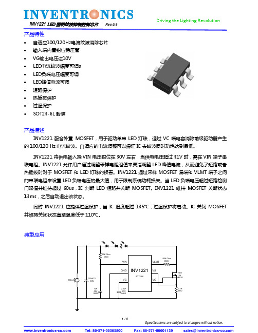
• 自适应100/120Hz 电流纹波消除芯片 • 输入端内置钳位稳压管 • VG 输出电压达10V • LED 电流纹波幅度可调s • LED 负端电压幅度可调 • LED 峰值电流可调 • 短路保护 • 热插拔保护 • 过温保护 •SOT23-6L 封装产品描述INV1221配合外置 MOSFET ,用于驱动单串LED 灯珠,通过VC 端电容消除前级驱动器产生的100/120 Hz 电流纹波。
自适应的电流调整可以保证IC 去纹波同时功耗达到最低。
INV1221将供电输入端VIN 电压钳位在30V 左右,当供电电压超过31V 时,需在VIN 端子串联电阻。
INV1221允许用户通过调整采样电阻阻值来灵活调整LED 峰值电流,从而避免了短路或者热插拔时对于MOSFET 和LED 灯珠的损害。
INV1221通过采样MOSFET 漏端和VLMT 端子之间的串联电阻来设置LED 负端电压的最大值,用于限制系统功耗损失。
当LED 负端电压超过短路检测门限值并维持超过60us ,IC 判断LED 短路并关断MOSFET 。
INV1221维持MOSFET 关断状态13ms ,之后自动退出该状态。
同时INV1221也提供过温保护,当IC 温度超过135℃,过温保护将启动。
IC 关闭MOSFET 并维持关闭状态直至温度低于110℃。
典型应用2A管脚排列图管脚说明(1)热阻注:(1)最大极限值是指超出该工作范围,芯片有可能损坏。
INV1221保证在-40°C150°C IC工作性能表现良好。
正常工作结温幅值由设计和相关参数批量数据统计得出。
(2)INV 1221集成用于避免芯片工作在过载情况下的温度保护功能。
当结温超过最大工作结温时,温度保护功能将启动。
连续工作在超出其极限参数的情况下,可能导致芯片损坏。
(3)以上参数在JESD51-7,2-layer PCB测得。
电气参数功能描述工作原理LED灯串和INV1221均由前级AC/DC电源提供驱动。


SM16159概述SM16159是LED 高密全彩屏专用驱动芯片,内置16K 的SRAM 存储结构,能够存储一帧完整显示数据,支持1~32扫LED 显示屏整帧数据存储及显示。
此方式降低了数据时钟频率,并可实现高灰阶效果。
SM16159内建16位灰阶控制的脉冲宽度调变功能,16个恒流输出通道所输出的电流值不受输出端负载电压的影响并提供一致且恒定的输出电流。
可通过选用外接电阻或调节6位电流增益来调整整体LED 的驱动电流。
封装信息特点◆ 内置64级电流增益调节功能 ◆ 内置16k SRAM ,支持1~32扫 ◆ 行扫倍频技术,刷新率提升2/4/8倍◆ 内置开路检测功能,解决开路“十字架”问题 ◆ 内置列下消影功能◆ 内置偏色、低灰麻点、第一扫偏暗改善功能 ◆ 16位PWM 灰阶控制可调显示刷新率SM_PWM专利技术◆ 工作电压:3.3V~5.0V◆ 输出恒流范围:0.6~32mA@VDD=5.0V ;0.6~24mA@VDD=3.3V ◆ 输出电流精度:通道间偏差:<±2.0%(最大值) 芯片间偏差:<±2.5%(最大值)管脚定义111213141516171819202122231098765432124OUT4OUT3OUT5OUT6OUT7OUT2OUT1OUT0LE DCLK SDI GND OUT8OUT9OUT10OUT11OUT12OUT13OUT14OUT15GCLK SDO REXT VDDS D ID DE X TD OC L KO U T OUT3OUT2OUT1OUT0LE OUT4C L KO U T G N DO U T O U T O U T内部功能框图LESDISDO管脚说明订购信息输出及输入等效电路GCLK,DCLK,SDI输入端LE输入端SDO输出端最大限定范围静态特性(V静态特性(V动态特性(V动态特性(V*在时序波形图(1)中,LE下降延后SDO的输出变化。


一、概述TM1650是一种带键盘扫描接口的LED(发光二极管显示器)驱动控制专用IC,内部集成有MCU 数字接口、数据锁存器、LED驱动、键盘扫描等电路。
本产品质量可靠、稳定性好、抗干扰能力强。
主要适用于机顶盒、家电设备(智能热水器、微波炉、洗衣机、空调、电磁炉)、电子称、智能电表等数码管,可适用于24小时长期连续工作的应用场合。
二、特性说明•两种显示模式(8段×4 位和 7 段×4 位)•支持单个按键7x4bit(28个按键)和组合按键(4个)• 8••高速2••••支持••三、四、管脚功能定义:1结束信号:保持CLK为“1”电平,DAT从“0”跳“1”,认为是结束信号,如(图1)E段;2、ACK信号如果本次通讯正常,芯片在串行通讯的第8个时钟下降沿后,TM1650主动把DAT拉低。
直到检测到CLK来了上升沿,DAT释放为输入状态(对芯片而言),如(图1)D段。
3、写“1”和写“0”写“1”:保持DAT为“1”电平,CLK从“0”跳到“1”,再从“1”跳到“0”,则认为是写入“1”如(图1)B段。
写“0”:保持DAT为“0”电平,CLK从“0”跳到“1”,再从“1”跳到“0”,则认为是写入“0”如(图1) C段。
4、 一个字节(8位)数据传输格式12345678B7B6B5B4B3B2B1B0DATCLK图2一个字节数据的传输格式如图2,数据发送时MSB 在前,LSB 在后,即高位先进。
微处理器的数据通过2线串行接口和TM1650通信,当CLK 是高电平时,DAT 上的信号必须保持不变;只有CLK 上的时钟信号为低电平时,DAT 上的信号才能改变。
数据输入的开始条件是CLK 为高电平时,DAT 由高变低;结束条件是CLK 为高时,DAT 由低电平变为高电平。
5、 写显示操作6SCL 7图5 读按键时序command :读按键命令4FH ;key_data :读按键数据(一个字节)。


led驱动芯片大全LED驱动芯片是指用于控制和驱动LED灯的电子元件。
随着LED技术的不断发展,LED驱动芯片也得到了广泛的应用。
下面将介绍一些常见的LED驱动芯片。
1. LM317: 这是一款常见的线性稳压器芯片,可用于驱动小功率的LED灯。
它具有良好的稳定性和低噪音特性。
2. PT4115: 这是一款高效的恒流LED驱动芯片,可用于驱动中功率的LED灯。
它具有宽输入电压范围、高达97%的转换效率和短路保护功能。
3. XL6009: 这是一款升压型DC-DC转换芯片,可用于驱动高亮度LED灯。
它具有宽输入电压范围、高达94%的转换效率和过流保护功能。
4. WS2812: 这是一款数字式LED驱动芯片,可用于驱动彩色LED灯。
它具有内置控制电路和存储器,能够实现多种色彩和灯效的变换。
5. TLC5940: 这是一款多路PWM输出型LED驱动芯片,可用于驱动多个LED灯。
它具有16路独立控制的PWM输出和电流控制功能。
6. AL9910: 这是一款高精度电流调节型LED驱动芯片,可用于驱动大功率LED灯。
它具有高达97%的转换效率和电流模式调光功能。
7. LT3754: 这是一款降压型DC-DC转换和恒流LED驱动芯片,可用于驱动多个串联LED灯。
它具有宽输入电压范围和高达97%的转换效率。
8. MAX16822: 这是一款高效、同步型的恒流LED驱动芯片,可用于驱动大功率LED灯。
它具有高达97%的转换效率和短路保护功能。
9. HV9961: 这是一款高压恒流LED驱动芯片,可用于驱动串联LED灯。
它具有宽输入电压范围、高达96%的转换效率和短路保护功能。
10. ILD600: 这是一款恒流LED驱动芯片,可用于驱动小功率LED灯。
它具有宽输入电压范围、过温保护和短路保护功能。
以上是一些常见的LED驱动芯片,它们具有不同的特点和适用范围。
在选择LED驱动芯片时,需要根据LED灯的功率和特性来进行选择,并注意选用符合安全标准的产品。


©2014 Whelen Engineering Company Inc.Form No.14818A (042816)For warranty information regarding this product, visit /warranty•Proper installation of this product requires the installer to have a good understanding of automotive electronics, systems and procedures.•Whelen Engineering requires the use of waterproof butt splices and/or connectors if that connector could be exposed to moisture.•Any holes, either created or utilized by this product, should be made both air- and watertight using a sealant recommended by your vehicle manufacturer.•Failure to use specified installation parts and/or hardware will void the product warranty.•If mounting this product requires drilling holes, the installer MUST be sure that no vehicle components or other vital parts could be damaged by the drilling process. Check both sides of the mounting surface before drilling begins. Also de-burr the holes and remove any metal shards or remnants. Install grommets into all wire passage holes.•If this manual states that this product may be mounted with suction cups, magnets, tape or Velcro®, clean the mounting surface with a 50/50 mix of isopropyl alcohol and water and dry thoroughly.•Do not install this product or route any wires in the deployment area of your air bag. Equipment mounted or located in the air bag deployment area will damage or reduce the effectiveness of the air bag, or become a projectile that could cause serious personal injury or death. Refer to your vehicle owner’s manual for the air bag deployment area. The User/Installer assumes full responsibility to determine proper mounting location, based on providing ultimate safety to all passengers inside the vehicle.•For this product to operate at optimum efficiency, a good electrical connection to chassis ground must be made. The recommendedprocedure requires the product ground wire to be connected directly to the NEGATIVE (-) battery post (this does not include products that use cigar power cords).•If this product uses a remote device for activation or control, make sure that this device is located in an area that allows both the vehicle and the device to be operated safely in any driving condition.•Do not attempt to activate or control this device in a hazardous driving situation.•This product contains either strobe light(s), halogen light(s), high-intensity LEDs or a combination of these lights. Do not stare directly into these lights. Momentary blindness and/or eye damage could result.•Use only soap and water to clean the outer lens. Use of other chemicals could result in premature lens cracking (crazing) and discoloration. Lenses in this condition have significantly reduced effectiveness and should be replaced immediately. Inspect and operate this product regularly to confirm its proper operation and mounting condition. Do not use a pressure washer to clean this product.•It is recommended that these instructions be stored in a safe place and referred to when performing maintenance and/or reinstallation of this product.•FAILURE TO FOLLOW THESE SAFETY PRECAUTIONS AND INSTRUCTIONS COULD RESULT IN DAMAGE TO THE PRODUCT OR VEHICLE AND/OR SERIOUS INJURY TO YOU AND YOUR PASSENGERS!A u t o m o t i v e : Warnings to InstallersWhelen’s emergency vehicle warning devices must be properly mounted and wired in order to be effective and safe. Read and follow all of Whelen’s written instructions when installing or using this device. Emergency vehicles are often operated under high speed stressful conditions which must be accounted for when installing all emergency warning devices. Controls should be placed within convenient reach of the operator so that they can operate the system without taking their eyes off the roadway. Emergency warning devices can require high electrical voltages and/or currents. Properly protect and use caution around live electrical connections.Grounding or shorting of electrical connections can cause high current arcing, which can cause personal injury and/or vehicle damage, including fire. Many electronic devices used in emergency vehicles can create or be affected by electromagnetic interference. Therefore, after installation of any electronic device it is necessary to test all electronic equipment simultaneously to insure that they operate free of interference from other components within the vehicle. Never power emergency warning equipment from the same circuit or share the same grounding circuit with radio communication equipment. All devices should be mounted in accordance with the manufacturer’s instructions and securely fastened to vehicle elements of sufficient strength to withstand the forces applied to the device. Driver and/or passenger air bags (SRS) will affect the way equipment should be mounted. This device should be mounted by permanent installation and within the zones specified by the vehicle manufacturer, if any. Any device mounted in the deployment area of an air bag will damage or reduce the effectiveness of the air bag and may damage or dislodge the device. Installer must be sure that this device, its mounting hardware and electrical supply wiring does not interfere with the air bag or the SRS wiring or sensors. Mounting the unit inside the vehicle by a method other than permanent installation is not recommended as unit may become dislodged during swerving; sudden braking or collision. Failure to follow instructions can result in personal injury. Whelen assumes no liability for any loss resulting from the use of this warning device. PROPER INSTALLATION COMBINED WITH OPERATOR TRAINING IN THE PROPER USE OF EMERGENCY WARNING DEVICES IS ESSENTIAL TO INSURE THE SAFETY OF EMERGENCY PERSONNEL AND THE PUBLIC.Warnings to UsersWhelen’s emergency vehicle warning devices are intended to alert other operators and pedestrians to the presence and operation of emergency vehicles and personnel. However, the use of this or any other Whelen emergency warning device does not guarantee that you will have the right-of-way or that other drivers and pedestrians will properly heed an emergency warning signal. Never assume you have the right-of-way. It is your responsibility to proceed safely before entering an intersection, driving against traffic, responding at a high rate of speed, or walking on or around traffic lanes. Emergency vehicle warning devices should be tested on a daily basis to ensure that they operate properly. When in actual use, the operator must ensure that both visual and audible warnings are not blocked by vehicle components (i.e.: open trunks or compartment doors), people, vehicles, or other obstructions. It is the user’s responsibility to understand and obey all laws regarding emergency warning devices. The user should be familiar with all applicable laws and regulations prior to the use of any emergency vehicle warning device. Whelen’s audible warning devices are designed to project sound in a forward direction away from the vehicle occupants. However, because sustained periodic exposure to loud sounds can cause hearing loss, all audible warning devices should be installed and operated in accordance with the standards established by the National Fire Protection Association.Safety FirstThis document provides all the necessary information to allow your Whelen product to be properly and safely installed. Before beginning the installation and/or operation of your new product, the installation technician and operator must read this manual completely. Important information is contained herein that could prevent serious injury or damage.WARNING: This product can expose you to chemicals including Methylene Chloride which is known to the State of California to cause cancer, and Bisphenol A, which is known to the State of California to cause birth defects or other reproductive harm. For more information go to .System Illustration:D.O.T. Defroster51 Winthrop RoadChester, Connecticut 06412-0684Phone: (860) 526-9504Internet: Salese-mail:*******************CustomerServicee-mail:*******************®ENGINEERING COMPANY INC.。