超小型5.5V DC-DC降压电源模块具备真6A性能
- 格式:pdf
- 大小:165.18 KB
- 文档页数:3

产品典型特性◆定电压输入,隔离非稳压输出,输出功率2W ◆转换效率高达86%◆小型SIP 封装◆无需外加元件◆隔离电压6000VDC◆工作环境温度:-40℃~+85℃◆塑料外壳,满足UL94-V0要求测试条件:如无特殊指定,所有参数测试均在标称输入电压、纯阻性额定负载及25℃室温环境下测得。
应用领域广泛应用于仪器仪表、通信、纯数字电路、一般低频模拟电路、继电器驱动电路、数据交换电路等领域产品选型列表产品型号输入电压范围(VDC)输出电压/电流(Vo/Io )输入电流(mA)标称电压最大容性负载纹波&噪声Max 效率(%)@输出满载,输入标称电压标称值范围电压(VDC)电流(mA )MAX./Min.满载typ.空载typ.uF mVp-p Min.Typ.FN2-05S05H654.5-5.554004742210001507981FN2-05S09H69222470254701508183FN2-05S12H612167519504701507577FN2-05S15H615133519504701507577FN2-05S24H62483506504701507779FN2-12S05H61210.8-13.254002001110001508082FN2-12S09H69222192134701508486FN2-12S12H6121671891310001508688FN2-12S15H6151331931710001508486FN2-24S05H62421.6-26.45400102810001507981FN2-24S12H6121679656801508486FN2-24S15H615133105154701508082FN2-24S24H6248398116801508385FN2-05D05H65 4.5-5.5±5±200481286801507476FN2-05D12H6±12±83425316801507981FN2-05D15H6±15±67519802201507678FN2-12D05H61210.8-13.2±5±200202126801508183FN2-12D09H6±9±110214354701507678FN2-12D12H6±12±83208352201507678FN2-12D15H6±15±671901410001508486FN2-24D05H62421.6±5±200111154701507577-26.4FN2-24D12H6±12±83104152201507880FN2-24D15H6±15±679810100015084861、“*”为开发中型号;2、为了确保该模块能够高效可靠的工作,使用时,其输出最小负载不能小于额定负载的10%。
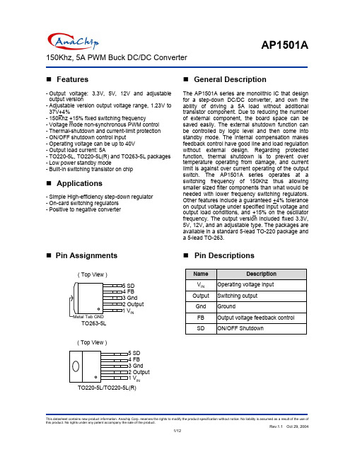
150Khz, 5A PWM Buck DC/DC ConverterFeatures- Output voltage: 3.3V, 5V, 12V and adjustable output version- Adjustable version output voltage range, 1.23V to 37V+4%- 150Khz +15% fixed switching frequency- Voltage mode non-synchronous PWM control - Thermal-shutdown and current-limit protection - ON/OFF shutdown control input - Operating voltage can be up to 40V - Output load current: 5A- TO220-5L, TO220-5L(R) and TO263-5L packages - Low power standby mode- Built-in switching transistor on chipApplications- Simple High-efficiency step-down regulator - On-card switching regulators - Positive to negative converterGeneral DescriptionThe AP1501A series are monolithic IC that design for a step-down DC/DC converter, and own the ability of driving a 5A load without additional transistor component. Due to reducing the number of external component, the board space can be saved easily. The external shutdown function can be controlled by logic level and then come into standby mode. The internal compensation makes feedback control have good line and load regulation without external design. Regarding protected function, thermal shutdown is to prevent over temperature operating from damage, and current limit is against over current operating of the output switch. The AP1501A series operates at a switching frequency of 150Khz thus allowing smaller sized filter components than what would be needed with lower frequency switching regulators. Other features include a guaranteed +4% tolerance on output voltage under specified input voltage and output load conditions, and +15% on the oscillator frequency. The output version included fixed 3.3V, 5V, 12V, and an adjustable type. The packages are available in a standard 5-lead TO-220 package and a 5-lead TO-263.Pin AssignmentsTO220-5L/TO220-5L(R)( Top View )( Top View )TO263-5LININPin DescriptionsNameDescriptionV IN Operating voltage input Output Switching output Gnd Ground FBOutput voltage feedback controlSD ON/OFF Shutdown150Khz, 5A PWM Buck DC/DC ConverterOrdering InformationT5: TO220-5LK5: TO263-5LBlank : Tube A : TapingBlank : Adjustable -33 : 3.3V -50 : 5.0V -12 : 12VT5R: TO220-5L(R)Blank : Normal L : Lead Free PackageBlock DiagramGndOutput V INSDFB150Khz, 5A PWM Buck DC/DC ConverterAbsolute Maximum RatingsSymbol ParameterRating Unit V CC Supply Voltage+45 V V SD ON/OFF Pin input voltage -0.3 to +25 V V FB Feedback Pin voltage -0.3 to +25V V OUT Output voltage to Ground -1V P D Power dissipationInternally limited WT ST Storage temperature -65 to +150 o C T OP Operating temperature -40 to +125 oCV OPOperating voltage+4.5 to +40VElectrical Characteristics (All Output Voltage Versions)Unless otherwise specified, V IN =12V for 3.3V, 5V, adjustable version and V IN =24V for the 12V version. I LOAD = 0.5ASymbol ParameterConditionsMin. Typ. Max. Unit 60I FBFeedback bias currentV FB =1.3V(Adjustable version only)40100nA127 150 173F OSC oscillator frequency 110 173 Khz1.6V SAT saturation voltage I OUT =5Ano outside circuitV FB =0V force driver on 1.51.7 VMax. Duty Cycle(ON) V FB =0V force driver on100DCMin. Duty cycle(OFF)V FB =12V force driver off0 %6.5I CL current limit peak current no outside circuitV FB =0 force driver on5.56.07.5 A Output = 0V no outside circuitV FB =12 force driver off 200 uAI LOutput =-1V Output leakage current V IN =40V 2 60 mA I Q Quiescent CurrentV FB =12 force driver off510mA 250I STBY Standby Quiescent CurrentON/OFF pin=5VV IN =40V150300 uAV IL Low (regulator ON) - 0.6 V IH ON/OFF pin logic input threshold voltageHigh (regulator OFF)2.0 1.3 - VI H ON/OFF pin logicinput currentV LOGIC =2.5V (OFF)15 25 I L ON/OFF pin input current V LOGIC =0.5V (ON)0.025uATO220-5L 2.5 ΘJC Thermal Resistance TO263-5L Junction to case 3.5 oC/WTO220-5L 28 ΘJAThermal Resistance With copper area of approximately 3 in 2TO263-5L Junction to ambient23oC/W150Khz, 5A PWM Buck DC/DC ConverterElectrical Characteristics (Continued)Specifications with boldface type are for full operating temperature range, the other type are for T J=25ºC.150Khz, 5A PWM Buck DC/DC ConverterTypical Performance CharacteristicsTypical Performance CharacteristicsNormalized Output Voltage4.904.955.005.055.10-50-25255075100125O U T P U T V O L T A G E C H A N G EJUNCTION TEMPERATURE(o C)JUNCTION TEMPERATURE(o C)S W I T C H C U R R E N T L I M I T (A )Switch Current Limit0.05.010.015.020.025.0-50-25255075100125JUNCTION TEMPERATURE(o C)S U P P L Y C U R R E N T (m A )Operating Quiescent CurrentInput VoltageE F F I C I E N C Y (%)Efficiency100657075808590958101520253035401.21.31.41.51.61.72.0345SWITCH CURRENT(A)S A T U R A T I O N V O L T A G E (V )Switch Saturation Voltage5.56.06.57.07.5-50-25255075100125SUPPLY VOLOTAGE (V)C U R R E N T (u A )0.040.080.0120.0160.0200.0Shutdown Quiescent Current10203040150Khz, 5A PWM Buck DC/DC ConverterTypical Performance Characteristics (Continued)JUNCTION TEMPERATURE(o C)B I A SC U R R E N T (n A )Feedback Pin Bias Current1.4510152022232425ON/OFF PIN VOLTAGE (V)C U R R E N T (u A )ON/OFF Pin Current (Sinking)0.030.060.090.0120.0150.00.010.020.030.040.050.0-50-252550751001250.01.02.03.04.05.0-50-25255075100125JUNCTION TEMPERATURE (o C)S U P P L Y V O L T A GE (V )Minimum Operating Supply VoltageJUNCTION TEMPERATURE (o C)T H R E S H O L D V O L T A G E (V )ON/OFF Threshold Voltage0.01.02.03.04.05.0-50-250255075100125Switch FrequencyJUNCTION TEMPERATURE (o C)F R E Q U E N C Y (k H z)0.050.0100.0150.0200.0-50-25255075100125150Khz, 5A PWM Buck DC/DC ConverterTypical Application Circuit(1) Fixed Type Circuit(2) Adjustable Type CircuitVout = V FB ×(1 +R2R1)V FB = 1.23V R2 = 1K ~ 3K(3) Delay Start CircuitR2150Khz, 5A PWM Buck DC/DC Converter Function DescriptionPin Functions+V INThis is the positive input supply for the IC switching regulator. A suitable input bypass capacitor must be present at this pin to minimize voltage transients and to supply the switching currents needed by the regulator.GroundCircuit ground.OutputInternal switch. The voltage at this pin switches between (+V IN – V SAT) and approximately – 0.5V, with a duty cycle of approximately V OUT / V IN. To minimize coupling to sensitive circuitry, the PC board copper area connected to this pin should be kept a minimum.FeedbackSenses the regulated output voltage to complete the feedback loop.ON/OFFAllows the switching regulator circuit to be shutdown using logic level signals thus dropping the total input supply current to approximately 150uA. Pulling this pin below a threshold voltage of approximately 1.3V turns the regulator on, and pulling this pin above 1.3V (up to a maximum of 25V) shuts the regulator down. If this shutdown feature is not needed, the ON/OFF pin can be wired to the ground pin or it can be left open, in either case the regulator will be in the ON condition. Thermal ConsiderationsThe AP1501A is available in two packages, a 5-pin TO-220 and a 5-pin surface mount TO-263.The TO-220 package needs a heat sink under most conditions. The size of the heatsink depends on the input voltage, the output voltage, the load current and the ambient temperature. The AP1501A junction temperature rises above ambient temperature for a 5A load and different input and output voltages. The data for these curves was taken with the AP1501A (TO-220 package) operating as a buck switching regulator in an ambient temperature of 25o C (still air). These temperature rise numbers are all approximate and there are many factors that can affect these temperatures. Higher ambient temperatures require more heat sinking.The TO-263 surface mount package tab is designed to be soldered to the copper on a printed circuit board. The copper and the board are the heat sink for this package and the other heat producing components, such as the catch diode and inductor. The PC board copper area that the package is soldered to should be at least 0.8 in2, and ideally should have 2 or more square inches of2 oz. Additional copper area improves the thermal characteristics, but with copper areas greater than approximately 6 in2, only small improvements in heat dissipation are realized. If further thermal improvements are needed, double sided, multilayer PC board with large copper areas and/or airflow are recommended.The AP1501A (TO-263 package) junction temperature rise above ambient temperature with a2A load for various input and output voltages. This data was taken with the circuit operating as a buck switching regulator with all components mounted ona PC board to simulate the junction temperature under actual operating conditions. This curve can be used for a quick check for the approximate junction temperature for various conditions, but be aware that there are many factors that can affect the junction temperature. When load currents higher than 3A are used, double sided or multilayer PC boards with large copper areas and/or airflow might be needed, especially for high ambient temperatures and high output voltages.For the best thermal performance, wide copper traces and generous amounts of printed circuit board copper should be used in the board layout. (Once exception to this is the output (switch) pin, which should not have large areas of copper.) Large areas of copper provide the best transfer of heat (lower thermal resistance) to the surrounding air, and moving air lowers the thermal resistance even further.150Khz, 5A PWM Buck DC/DC ConverterFunction Description (Continued)Package thermal resistance and junction temperature rise numbers are all approximate, and there are many factors that will affect these numbers. Some of these factors include board size, shape, thickness, position, location, and even board temperature. Other factors are, trace width, total printed circuit copper area, copper thickness, single or double-sided, multilayer board and the amount of solder on the board. The effectiveness of the PC board to dissipate heat also depends on the size, quantity and spacing of other components on the board, as well as whether the surrounding air is still or moving.Furthermore, some of these components such as the catch diode will add heat to the PC board and the heat can vary as the input voltage changes. For the inductor, depending on the physical size, type of core material and the DC resistance, it could either act as a heat sink taking heat away from the board, or it could add heat to the board.Marking Information(1) TO263-5L1501AXX Output Type:1501: ADJ 1501A33: 3.3V 1501A50: 5.0V 1501A12: 12V( Top view )"02" = 2002"01" = 2001~(2) TO220-5L1501AXX Output Type:1501: ADJ 1501A12: 12V( Top view )"02" = 2002"01" = 2001~150Khz, 5A PWM Buck DC/DC ConverterPackage Information(1) Package Type: TO220-5LDimensions In Millimeters Dimensions In Inches SymbolMin. Nom. Max. Min. Nom. Max.A 4.07 4.45 4.82 0.160 0.175 0.190b 0.76 0.89 1.02 0.030 0.035 0.040C 0.36 0.50 0.64 0.014 0.020 0.025D 14.22 14.86 15.50 0.560 0.585 0.610E 9.78 10.16 10.54 0.385 0.400 0.415e 1.57 1.71 1.85 0.062 0.067 0.073e1 6.68 6.81 6.93 0.263 0.268 0.273F 1.14 1.27 1.40 0.045 0.050 0.055H1 5.46 6.16 6.86 0.215 0.243 0.270J1 2.29 2.74 3.18 0.090 0.108 0.125L 13.21 13.97 14.73 0.520 0.550 0.580Øp 3.68 3.81 3.94 0.145 0.150 0.155Q 2.54 2.73 2.92 0.100 0.107 0.115150Khz, 5A PWM Buck DC/DC ConverterPackage Information (Continued)(2) Package Type: TO263-5LLand Pattern Recommendation (Unit: mm)Dimensions In Millimeters Dimensions In InchesSymbolMin. Nom. Max. Min. Nom. Max.A 4.07 4.46 4.85 0.160 0.176 0.191B 0.66 0.84 1.02 0.026 0.033 0.040C 0.36 0.50 0.64 0.014 0.020 0.025 C2 1.14 1.27 1.40 0.045 0.050 0.055D 8.65 9.15 9.65 0.341 0.360 0.380E 9.78 10.16 10.54 0.385 0.400 0.415 e 1.57 1.71 1.85 0.062 0.068 0.073 L 14.61 15.24 15.88 0.575 0.600 0.625 L1 2.29 2.54 2.79 0.090 0.100 0.110 L2 - - 2.92 - - 0.115150Khz, 5A PWM Buck DC/DC ConverterPackage Information (Continued)(3) Package Type: TO220-5L(R) Mechanical drawingH3Dimensions In Millimeters Dimensions In Inches SymbolMin. Nom. Max. Min. Nom. Max.A 4.4 4.6 4.7 0.175 0.180 0.185 b 0.7 0.8 0.9 0.027 0.032 0.037 D 8.4 8.7 8.9 0.330 0.340 0.350 d1 1.0 0.039 d2 6.3 0.248 E 9.91 10.16 10.41 0.390 0.400 0.410 e 1.6 1.7 1.8 0.062 0.067 0.072 F 1.2 1.25 1.3 0.048 0.050 0.052 H1 6.4 0.250 H2 20.8 21.6 22.4 0.820 0.850 0.880 H3 23.9 24.7 25.5 0.942 0.972 1.002 J1 2.7 0.105 J2 3.7 4.5 5.3 0.147 0.177 0.207 J3 8.4 0.331 Q 2.5 2.8 3.0 0.100 0.110 0.120。

该手册版权和解释权为常州能动电子科技有限公司所有第1页共2页EF05-400系列-----高压输入小体积DC-DC 模块电源5W产品特性◆宽压输入65~650VDC ◆隔离电压高达4KVAC◆保护功能齐全(输入过压、输出短路等)◆高效率、高功率密度、低纹波系数◆高可靠电源管理芯片方案◆工业级产品设计应用范围高电压输入,超宽电压输入范围,产品广泛应用于电力仪表、载波通讯等领域。
产品型号型号输出Vo1(VDC/mA)输出Vo1(VDC/mA)效率(TYP)EF05-400E12X712VDC /300mA7.5VDC /100mA70%注:1.★研发中型号2.如有其它规格型号需求,可直接联系我司。
输入特性输入电压范围65~650VDC 输入电流(Vin=300VDC)<0.05A (TYP)外接保险丝1A/250V慢断输出特性输出电压稳压精度(主路)±2%源效应±0.5%(typ)负载调整率(10%~100%)±1%(typ)最小负载10%输出纹波+噪声(峰-峰值)1%Vo(typ)(20MHz Bandwidth)短路保护可长期短路,自恢复一般特性温度特性工作温度功率降额存储温度-40℃~+75℃3.75%/℃,-40℃~+85℃该手册版权和解释权为常州能动电子科技有限公司所有第2页共2页湿度90%RH(max)温漂<0.03%/℃开关频率80kHz(typ)耐压输入--Vo13000VAC 输入--Vo24000VAC Vo1--Vo24000VAC 漏电流<1mA,一分钟安全等级CLASS Ⅰ封装形式裸板PCB 安装插针端子注:1.以上所列数据除特别说明外,都是在TA=25℃,湿度<75%的条件下测得;2.采用平行线测试法测试。
单位:mm误差:±0.25mmIN+EN Vo1+Vo1-Vo2+输入NP12V 输出7.5V。


180KHz 60V 5A 开关电流升压/升降压型DC-DC转换器XL6019特点⏹5V到40V宽输入电压范围⏹单个反馈引脚控制正或负输出电压⏹电流模式控制提供出色的瞬态响应⏹ 1.25V输出电压采样电压⏹固定180KHz开关频率⏹最大5A开关电流⏹SW内置过压保护功能⏹出色的线性与负载调整率⏹EN脚TTL关断功能⏹内置功率MOS⏹94%以上转换效率⏹内置频率补偿功能⏹内置软启动功能⏹内置热关断功能⏹内置限流功能⏹TO263-5L封装应用⏹EPC/笔记本车载适配器⏹升压、升降压转换⏹手持式设备供电描述XL6019是一款专为升压、升降压设计的单片集成电路,可工作在DC5V到40V输入电压范围,低纹波,内置功率MOS。
XL6019内置固定频率振荡器与频率补偿电路,简化了电路设计。
PWM控制环路可以调节占空比从0~90%之间线性变化。
内置过电流保护功能与EN脚逻辑电平关断功能。
图1. XL6019封装180KHz 60V 5A 开关电流升压/升降压型DC-DC 转换器 XL6019引脚配置FB SW EN GNDVIN 12345TO263-5L图2. XL6019引脚配置表1.引脚说明引脚号 引脚名 描述1 GND 接地引脚。
2 EN 使能引脚,低电平关机,高电平工作,悬空时为高电平。
3 SW 功率开关输出引脚,SW 是输出功率的开关节点。
4 VIN 电源输入引脚,支持5V 到40V DC 范围电压输入,需要在VIN 与GND 之间并联电解电容以消除噪声。
5FB输出电压采样引脚,FB 参考电压为1.25V 。
180KHz 60V 5A 开关电流升压/升降压型DC-DC 转换器 XL6019方框图3.3V Regulator 1.25V ReferenceSWGND3.3V 1.25VEACOMPOscillator 180KHzDriverFBOVPNDMOSENOCPRS LatchThermal ShutdownSlop CompensationPhase CompensationUVLOSoft StartVIN图3. XL6019方框图典型应用XL6019C1105VIN41253GNDVINSWEN ON OFF Boost Converter Input 12V ~ 22V Output 24V / 1.5AVOUT=1.25*(1+R2/R1)D1 MBRD1045R12.7K 1%COUT220uF/35VR249.9K 1%CIN220uF/35VC2105FB图4. XL6019系统参数测量电路180KHz 60V 5A开关电流升压/升降压型DC-DC转换器XL6019订购信息产品型号打印名称封装方式环保认证包装类型XL6019E1 XL6019E1 TO263-5L RoHS & HF 800只每卷绝对最大额定值(注1)参数符号值单位输入电压Vin -0.3到45 V-0.3到Vin V反馈引脚电压VFB-0.3到Vin V使能引脚电压VEN-0.3到60 V输出开关引脚电压VSW内部限制mW功耗PD热阻(TO263-5L)R JA30 o C/W (结到环境,无外部散热片)最大结温T-40到150 o CJ-40到125 o C操作结温TJ贮存温度范围T-65到150 o CSTG引脚温度(焊接10秒) T260 o CLEADESD (人体模型) >2000 V注1:超过绝对最大额定值可能导致芯片永久性损坏,在上述或者其他未标明的条件下只做功能操作,在绝对最大额定值条件下长时间工作可能会影响芯片的寿命。

一块高端工业控制终端好选择 —— SK-AM64评估套件测评近几年嵌入式最火的领域,各种工控网关终端绝对算得上一个。
智能家电和工控设备更新换代,对控制终端提出了越来越多的要求,各老牌大厂都不断在更新自己的方案。
目前对这个领域的方案主要需求是更高的安全性、更高的集成度、更高的稳定性、更强的性能,但是开发者如何选择一款合适的方案并非易事。
德州仪器(TI)新推出的AM64X系列方案绝对是目前此领域非常不错的的代表,这次就由我带大家了解一下基于AM64x处理器的评估套件SK-AM64。
开箱视频一、开箱SK-AM64评估套件使用纸质外盒包装,包装盒正面印着产品型号,背面是评估板板载资源的列表和简单的使用说明。
打开盒子可以看到由防静电袋装着开发板。
AM64x 入门套件是一个完整测试和开发平台,适合用于加速原型设计。
套件包括:有线和无线连接、三个扩展头、多个引导选项和灵活的调试功能。
配有TI 的AM64x 处理器和优化的功能集,允许用户使用基于以太网的接口、USB 接口、有线串行接口以及2.4GHz 和5GHz 无线通信来创建商业和工业解决方案。
两个板载1Gbps 以太网端口用于有线连接,此外还有三个扩展头用于扩展板功能。
此套件采用标准串行协议(如UART、I²C 和SPI),可用作通信网关与多个其他器件进行连接。
该入门套件可通过在A53 内核上运行Linux 进行评估,从而可作为远程工业通信网络中的中央引擎,也适合用作可编程逻辑控制器或运动控制器。
额外的嵌入式仿真逻辑允许使用标准开发工具(例如TI 的Code Composer Studio™)进行仿真和调试。
特性•软件:TI Processor SDK Linux/RT Linux/RTOS内核、Yocto文件系统、包含Wi-Fi® 的开箱即用例程•处理:AM64x,含2 个Arm Cortex-A53、4 个Arm Cortex-R5F、1个可以做安全功能使用的M4F,2 个PRU_ICSSG•通过 WiLink™8 WL1837MOD 模块实现双频带Wi-Fi®、Bluetooth®/低功耗蓝牙 5.1;2 个1000/100Mbps RJ-45 以太网接口•连接:可通过micro-USB 连接1 个Type A USB 3.1 gen1(超高速)、板载XDS110 JTAG 仿真器和 3 个UART•扩展和原型设计:40 引脚Raspberry Pi (RPI4) HAT、PRU-ICSSG 实时I/O 和TI-MCU 头•存储: 2GB LPDDR4;SK 上的可引导接口:可移除uSD、USB、16MB OSPI、以太网、UART开发需要自配的硬件•USB-C 5V 3A 电源•USB SD 卡写入器•Micro-SD 卡(16GB 或更大)•用于UART 串行通信的USB Micro-B 电缆•以太网电缆(可选)二、硬件描述此评估板集成了丰富的扩展接口,并且都是目前最流行的扩展接口,比如集成了兼容Raspberry Pi的扩展接口,这将能适配目前Raspberry Pi种类丰富的第三方外设模块,这将简化原型设计的难度而且更具可玩性,让开发者快速验证自己的创意。
5W,DIY型AC-DC 模块电源CB RoHS产品特点●超宽输入电压范围:85-305VAC/70-430VDC ●交直流两用(同一端子输入电压)●工作温度范围:-40℃to +85℃●百搭应用、布局灵活●超小体积、高功率密度、绿色环保●寿命可控、成本可调●空载功耗0.1W ●输出短路、过流保护●符合IEC/EN61558、IEC/EN60335标准●通过IEC/EN/UL62368认证LS05-13BxxR3系列-----是金升阳为客户提供的小型化裸板的高效绿色模块电源,该型号电源具有交直流两用、输入电压范围宽、高可靠性、低功耗、安全隔离等优点。
广泛适用于工控和电力仪器仪表、智能家居等对体积要求苛刻、并对EMC 要求不高的场合,如果需要应用于电磁兼容恶劣的环境下必须添加EMC 外围电路。
输入特性项目工作条件Min.Typ.Max.单位输入电压范围交流输入85--305VAC 直流输入70--430VDC 输入频率47--63Hz输入电流115V AC ----0.2A230V AC ----0.1冲击电流115V AC --20--230V AC--40--外接保险丝推荐值推荐1A ,慢断型,必接(实际使用时需根据应用环境选择)热插拔不支持输出特性项目工作条件Min.Typ.Max.单位输出电压精度10%-100%负载--±5--%线性调节率额定负载--±1.5--负载调节率10%-100%负载--±3--纹波噪声*20MHz 带宽(峰-峰值),10%-100%负载--80150mV 温度漂移系数--±0.15--%/℃待机功耗230V AC--0.100.15W短路保护打嗝式,可长期短路,自恢复选型表认证产品型号输出功率标称输出电压及电流(Vo/Io)效率(230VAC,%/Typ.)最大容性负载(uF)CE/UL/CBLS05-13B03R3 3.3W3.3V/1000mA 692200LS05-13B05R35W5V/1000mA 761500LS05-13B09R39V/560mA 77680LS05-13B12R312V/420mA 79470LS05-13B15R315V/340mA 79330LS05-13B24R324V/210mA81100注:1.标称输出电压指经外围后加到负载端电压;2.若产品使用在剧烈振动环境下,需点胶固定其本体。
GM2001无电感5V输出电荷泵型降压稳压芯片1、产品简介GM2001是一款5V输出电荷泵型降压稳压芯片,输入电压范围宽达6~28V,最大输出电流能力达150mA,内部采用固定900KHz开关频率,同时芯片内部还集成了短路保护、过流保护、过热保护等单元提升可靠性,ESD HBM高达±6000V。
与传统的降压芯片相比,GM2001无需外围的电感和肖特基二极管,应用方案简洁,仅需要3个外围电容。
同时由于无电感器件,芯片的EMI要大幅度低于有电感的开关电源方案,并且在输出电压纹波方面也具有优越的性能。
而与LDO类型的稳压芯片相比,GM2001在效率方面具有极高优势,当输入电压高于10.5V时,转换效率会增加一倍,最高转换效率高达81%,但输出电压噪声又不会增加过多,因此GM2001可以直接取代LDO。
尤其在智能电表和水表及其通信模块等工业领域,GM2001是一款具有优越性价比的稳压电源芯片。
2、应用范围■工业控制■电表、水表、气表■汽车电子3、特色■工作电压:6~28V■输出电压:5V±5%■输出电流:150mA max■ESD HBM±6KV■固定频率:900KHz■低纹波:<8mV■过流保护■过热保护■短路保护■温度范围-40℃to+85℃■应用成本低:无需电感、肖特基二极管、外围器件极少4、封装类型■EMSOP85、功能引脚定义图1、GM2001Top View 序号名称说明1VIN输入引脚2NC3GND接地4CP飞电容正端5CN飞电容负端6NC7NC8VOUT输出引脚注意:EP必须在PCB设计时接露铜散热区6、典型应用电路图2典型应用电路图7、极限参数符号说明大小单位VCC最大输入端电压30VTj最大结温170℃Θja热阻40℃/W Tstg储存温度-60~160℃Pd最大消耗功率(ESOP8) 1.5WESD HBM6000V8、电气特性(各外围参数如图2所示,VDD=12V,TA=+25℃,除非特别注明)参数符号条件最小典型最大单位输入电压VCC628V输出电压VOUT VCC:7~28V 4.75 5.3V电压精度△Vout±5%静态电流Iin空载 1.1mA输出电流Iout100150mA负载调整Vrl负载电流0~100mA 3.7mV/mA 负载电流50~100mA1mV/mA 输入调整Vri VCC:7~28V1mV/V 开关频率Fosc900KHz电源抑制PSRR1Hz~10Mhz50dB输出纹波Riple负载电流=100mA57mV负载电流=15mA1mV短路电流Ishort输出短路到地22mA过流保护Ip200mA热保护点Tp150℃Thys20℃热保护迟滞9、典型特性图3、转换效率VS.输入电压(Iout=100mA)图4、转换效率VS.输出电流(VIN=12V)图5、输入端纹波(Iout=100mA)图6、输出端纹波(Iout=100mA)图7、负载响应CH1:Iout25mA/Div CH2:Vout20mV/Div100us/Div图8、输入响应图9、开关频率VS.温度图10、电源抑制比图11、输出纹波频谱(Iout=100mA)图12、输出纹波频谱(Iout=10mA)10、应用说明概述GM2001是一款电荷泵降压型稳压芯片,可以提供稳定的5V输出,最大输出电流能力达150mA。
超小型5.5V DC/DC降压电源模块具备真6A性能
TI超小型5.5V DC/DC降压电源模块TPSM82480
集持续6A供能与95%高效率于一身。
德州仪器近日推出了一款5.5V降压型电源模块,可提供真正的持续6A 输出电流和高达95%的效率。
易用的TPSM82480 DC/DC模块将功率金属氧化物半导体场效应晶体管(MOSFET)和屏蔽电感集成到一个小尺寸封装中,用于空间和高度受限的应用。
例如负载点电信、网络、测试和测量电源。
超小型5.5V DC/DC降压电源模块具备真6A性能
TI高度集成的TPSM82480在整个温度范围内保持所需的6A输出电流,无需额外的气流。
这是通过使用两相控制拓扑来实现的,该拓扑共享各相之间的负载以确保高效率和均流操作。
其他功能还包括可调节软启动、支持多级处理器的电压选择(VSEL),以及电源状态良好指示。