
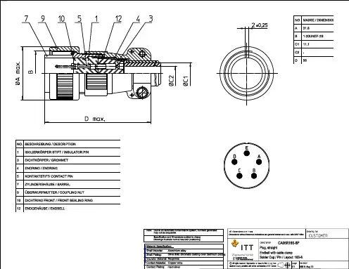
CA06R16S-8P;中文规格书,Datasheet资料
- 格式:pdf
- 大小:246.71 KB
- 文档页数:2
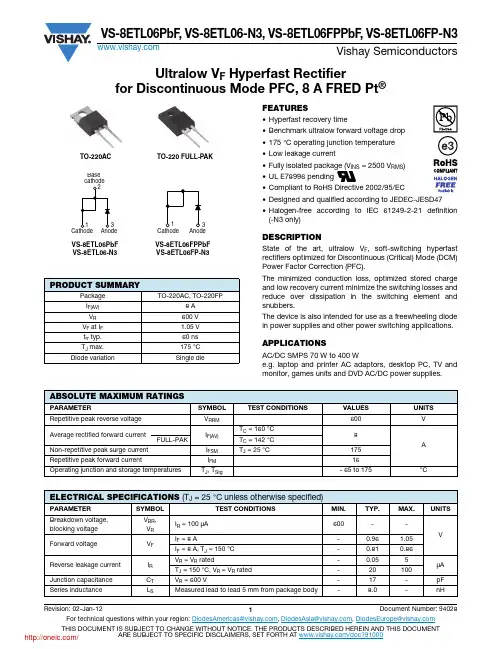
Ultralow V F Hyperfast Rectifierfor Discontinuous Mode PFC, 8 A FRED Pt ®FEATURES•Hyperfast recovery time•Benchmark ultralow forward voltage drop •175 °C operating junction temperature•Low leakage current•Fully isolated package (V INS = 2500 V RMS )•UL E78996 pending•Compliant to RoHS Directive 2002/95/EC•Designed and qualified according to JEDEC-JESD47•Halogen-free according to I EC 61249-2-21 definition (-N3 only)DESCRIPTIONState of the art, ultralow V F , soft-switching hyperfast rectifiers optimized for Discontinuous (Critical) Mode (DCM)Power Factor Correction (PFC).The minimized conduction loss, optimized stored charge and low recovery current minimize the switching losses and reduce over dissipation in the switching element and snubbers.The device is also intended for use as a freewheeling diode in power supplies and other power switching applications.APPLICATIONSAC/DC SMPS 70 W to 400 We.g. laptop and printer AC adaptors, desktop PC, TV and monitor, games units and DVD AC/DC power supplies.PRODUCT SUMMARYPackage TO-220AC, TO-220FPI F(AV)8 A V R 600 V V F at I F 1.05 V t rr typ.60 ns T J max.175 °C Diode variationSingle dieTO-220ACTO-220 FULL-PAKABSOLUTE MAXIMUM RATINGSPARAME ER SYMBOL T ES T CONDI T IONS VALUES UNI T S Repetitive peak reverse voltage V RRM 600VAverage rectified forward current I F(AV)T C = 160 °C 8A FULL-PAKT C = 142 °C Non-repetitive peak surge current I FSM T J = 25 °C175Repetitive peak forward currentI FM 16Operating junction and storage temperaturesT J , T Stg- 65 to 175°C ELECTRICAL SPECIFICATIONS (T J = 25 °C unless otherwise specified)PARAME T ER SYMBOLT ES T CONDI T IONS MIN. T YP. MAX. UNI T S Breakdown voltage,blocking voltage V BR ,V R I R = 100 μA 600--VForward voltage V F I F = 8 A-0.96 1.05I F = 8 A, T J = 150 °C -0.810.86Reverse leakage current I R V R = V R rated-0.055μA T J = 150 °C, V R = V R rated -20100Junction capacitance C T V R = 600 V-17-pF Series inductance L SMeasured lead to lead 5 mm from package body-8.0-nHFig. 1 - Typical Forward Voltage Drop CharacteristicsReverse VoltageDYNAMIC RECOVERY CHARACTERISTICS (T C = 25 °C unless otherwise specified)PARAME T ER SYMBOL T ES T CONDI T IONS MIN. T YP. MAX. UNI T SReverse recovery timet rrI F = 1 A, dI F /dt = 100 A/μs, V R = 30 V-60100nsI F = 8 A, dI F /dt = 100 A/μs, V R = 30 V -150250T J = 25 °C I F = 8 AdI F /dt = 200 A/μs V R = 390 V-170-T J = 125 °C-250-Peak recovery current I RRM T J = 25 °C -15-A T J = 125 °C -20-Reverse recovery chargeQ rrT J = 25 °C - 1.3-μC T J = 125 °C- 2.6-THERMAL - MECHANICAL SPECIFICATIONSPARAME ER SYMBOL T ES T CONDI T IONS MIN. T YP. MAX. UNI T S Maximum junction and storage temperature range T J , T Stg - 65-175°CThermal resistance,junction to caseR thJC - 1.42°C/W (FULL-PAK)- 3.4 4.3Thermal resistance,junction to ambient per leg R thJA Typical socket mount--70Thermal resistance,case to heatsink R thCSMounting surface, flat, smooth and greased-0.5-Weight- 2.0-g -0.07-oz.Mounting torque 6.0(5.0)-12(10)kgf · cm (lbf · in)Marking deviceCase style TO-220AC 8ETL06Case style TO-220 FULL-PAK8ETL06FPFig. 3 - Typical Junction Capacitance vs. Reverse VoltageFig. 4 - Maximum Thermal Impedance Z thJC CharacteristicsFig. 5 - Maximum Thermal Impedance Z thJC Characteristics (FULL-PAK)Fig. 6 - Maximum Allowable Case Temperature vs.Average Forward CurrentFig. 7 - Maximum Allowable Case Temperature vs.Average Forward Current (FULL-PAK)Fig. 8 - Forward Power Loss CharacteristicsFig. 9 - Typical Reverse Recovery Time vs. dI F /dtFig. 10 - Typical Stored Charge vs. dI F /dtNote(1)Formula used: T C = T J - (Pd + Pd REV ) x R thJC ;Pd = Forward power loss = I F(AV) x V FM at (I F(AV)/D) (see fig. 8); Pd REV = Inverse power loss = V R1 x I R (1 - D); I R at V R1 = Rated V RFig. 11 - Reverse Recovery Parameter Test CircuitFig. 12 - Reverse Recovery Waveform and DefinitionsORDERING INFORMATION TABLEORDERING INFORMATION (Example)PREFERRED P/N QUANTITY PER T/R MINIMUM ORDER QUANTITY PACKAGING DESCRIPTION VS-8ETL06PbF501000Antistatic plastic tubeVS-8ETL06-N3501000Antistatic plastic tubeVS-8ETL06FPPbF501000Antistatic plastic tubeVS-8ETL06FP-N3501000Antistatic plastic tubeLINKS TO RELATED DOCUMENTSDimensions TO-220AC /doc?95221 TO-220FP /doc?95005Part marking information TO-220ACPbF /doc?95224 /doc?95068 TO-220FPPbF /doc?95009 /doc?95440Outline Dimensions Vishay SemiconductorsDIMENSIONS in millimetersDocument Number: 95221For technical questions within your region, please contact one of the following:Revision: 07-Mar-11DiodesAmericas@ , DiodesAsia@ , DiodesEurope@1TO-220ACOutline DimensionsVishay SemiconductorsDIMENSIONS in millimeters and inchesNotes(1)Dimensioning and tolerancing as per ASME Y14.5M-1994(2)Lead dimension and finish uncontrolled in L1(3)Dimension D, D1 and E do not include mold flash. Mold flash shall not exceed 0.127 mm (0.005") per side. These dimensions are measured at the outermost extremes of the plastic body(4)Dimension b1, b3 and c1 apply to base metal only (5)Controlling dimension: inches(6)Thermal pad contour optional within dimensions E, H1, D2 and E1(7)Dimension E2 x H1 define a zone where stamping and singulation irregularities are allowed(8)Outline conforms to JEDEC TO-220, D2 (minimum) where dimensions are derived from the actual package outlineSYMBOLMILLIMETERS INCHES NOTES SYMBOLMILLIMETERS INCHES NOTES MIN.MAX.MIN.MAX.MIN.MAX.MIN.MAX.A 4.25 4.650.1670.183E1 6.868.890.2700.3506A1 1.14 1.400.0450.055E2-0.76-0.0307A2 2.56 2.920.1010.115e 2.41 2.670.0950.105b 0.69 1.010.0270.040e14.885.280.1920.208b10.380.970.0150.0384H16.09 6.480.2400.2556, 7b2 1.20 1.730.0470.068L 13.5214.020.5320.552b3 1.14 1.730.0450.0684L1 3.32 3.820.1310.1502c 0.360.610.0140.024L3 1.78 2.130.0700.084c10.360.560.0140.0224L40.76 1.270.0300.0502D 14.8515.250.5850.6003Ø P 3.54 3.730.1390.147D18.389.020.3300.355Q 2.603.000.1020.118D211.6812.880.4600.507690° to 93°90° to 93°E10.1110.510.3980.4143, 6Legal Disclaimer Notice VishayDisclaimerALL PRODU CT, PRODU CT SPECIFICATIONS AND DATA ARE SU BJECT TO CHANGE WITHOU T NOTICE TO IMPROVE RELIABILITY, FUNCTION OR DESIGN OR OTHERWISE.Vishay Intertechnology, Inc., its affiliates, agents, and employees, and all persons acting on its or their behalf (collectively,“Vishay”), disclaim any and all liability for any errors, inaccuracies or incompleteness contained in any datasheet or in any other disclosure relating to any product.Vishay makes no warranty, representation or guarantee regarding the suitability of the products for any particular purpose or the continuing production of any product. To the maximum extent permitted by applicable law, Vishay disclaims (i) any and all liability arising out of the application or use of any product, (ii) any and all liability, including without limitation special, consequential or incidental damages, and (iii) any and all implied warranties, including warranties of fitness for particular purpose, non-infringement and merchantability.Statements regarding the suitability of products for certain types of applications are based on Vishay’s knowledge of typical requirements that are often placed on Vishay products in generic applications. Such statements are not binding statements about the suitability of products for a particular application. It is the customer’s responsibility to validate that a particular product with the properties described in the product specification is suitable for use in a particular application. Parameters provided in datasheets and/or specifications may vary in different applications and performance may vary over time. All operating parameters, including typical parameters, must be validated for each customer application by the customer’s technical experts. Product specifications do not expand or otherwise modify Vishay’s terms and conditions of purchase, including but not limited to the warranty expressed therein.Except as expressly indicated in writing, Vishay products are not designed for use in medical, life-saving, or life-sustaining applications or for any other application in which the failure of the Vishay product could result in personal injury or death. Customers using or selling Vishay products not expressly indicated for use in such applications do so at their own risk and agree to fully indemnify and hold Vishay and its distributors harmless from and against any and all claims, liabilities, expenses and damages arising or resulting in connection with such use or sale, including attorneys fees, even if such claim alleges that Vishay or its distributor was negligent regarding the design or manufacture of the part. Please contact authorized Vishay personnel to obtain written terms and conditions regarding products designed for such applications.No license, express or implied, by estoppel or otherwise, to any intellectual property rights is granted by this document or by any conduct of Vishay. Product names and markings noted herein may be trademarks of their respective owners.Material Category PolicyVishay Intertechnology, Inc. hereb y certifies that all its products that are identified as RoHS-Compliant fulfill the definitions and restrictions defined under Directive 2011/65/EU of The European Parliament and of the Council of June 8, 2011 on the restriction of the use of certain hazardous substances in electrical and electronic equipment (EEE) - recast, unless otherwise specified as non-compliant.Please note that some Vishay documentation may still make reference to RoHS Directive 2002/95/EC. We confirm that all the products identified as being compliant to Directive 2002/95/EC conform to Directive 2011/65/EU.Revision: 12-Mar-121Document Number: 91000分销商库存信息:VISHAY8ETL06FPPBF8ETL068ETL06FP。

船用主机8PC2-6/2L柴油机技术规格书陕西柴油机重工有限公司目录第一章、总则第二章、柴油机主要技术参数第三章、制造及验收第四章、供货范围第五章、色彩及铭牌第六章、油封和包装第七章、培训和售后服务附件一、运行区域曲线附件二、随机仪表清单附件三、随机备件清单附件四、随机工具清单第一章总则1.本技术规格书规定了船用主机8PC2-6L柴油机的技术性能、供货范围、质量保证、交货验收等内容,是柴油机制造、验收和交货的主要依据。
2. 本技术规格书是根据法国S.E.M.T提供的技术文件及企业的相关标准编制而成,引用的主要标准有:《钢制海船入级与建造规范(2002版)》GB1105.1-87 内燃机台架性能试验方法标准环境状况及功率燃油消耗和滑油消耗的标定GB1147-87 内燃机通用技术条件GB5741-85 船用柴油机排气烟度测量方法GB6301-86 船用柴油机燃油消耗测定方法GB/T14363-93 柴油机机油消耗测定方法CB*3154-83 船用柴油机振动测量方法CB*3256-85 船用柴油机振动评级CB/T3253-94 船用柴油机技术条件CB/T3254.2-94 船用柴油机台架试验试验方法法国国家标准(NF)及中国国家标准(GB)法国热机协会标准(NSE)制造厂企业标准(Q/SC)GB8840 船用柴油机排气烟度限制GB/T19001-2000 质量管理体系第二章主要技术参数1. 柴油机可在下列环境中正常运行:横倾:±15°;横摇:±22.5°;纵倾:±5°;纵摇:±7.5°环境温度:45℃大气压力:100Kpa空气相对湿度:≤95%冷却海水进机最高温度:32℃有盐雾、油雾、霉菌和正常航行所产生的震动和冲击2、接口柴油机与外界系统接口见柴油机总体布置图3、主要技术参数(1) 型号: 8PC2-6L(M.P.C增压)(2) 型式:直列式、四冲程、不可逆转、增压器空冷器位于输出端、机不带泵(淡水泵、海水泵、滑油泵和燃油输送泵)(3) 气缸直径: 400mm(4) 活塞行程: 460mm(5) 气缸数: 8(6) 气缸中心距: 740mm(7) 几何压缩比: 11.4(8) 发火顺序: 1-5-7-3-8-4-2-6-1从输出端看曲轴顺时针旋转(9) 柴油机额定功率的标准环境条件:吸入空气温度: 27℃大气压力: 100KPa空冷器进口冷却水温度: 27℃排气背压:≤2.5KPa进气真空度:≤2.5Kpa燃油低热值 42700Kj/Kg(10) 功率标准环境条件下,柴油机输出法兰后最大持续功率(MCR): 4400KW持续使用功率(CSR): 3960KW(90%MCR)超负荷功率(110%MCR): 4840KW(每12小时内允许1小时)(11) 转速a.最大持续功率(MCR)时的转速: 520转/分b.超负荷功率时的转速:536转/分c.最低稳定转速:200转/分(12) 在标准环境条件下,最大持续功率时的性能参数:平均有效压力: 2190KPa活塞平均速度: 7.97m/s进气流量: 6.8kg/kwh排气流量: 7.0kg/kwh排气阀后平均排气温度: 450±50℃,两缸间温差≤80℃涡轮进口废气温度:≤650℃增压器后排气温度:≤400℃±20℃进气总管内增压空气压力: 230Kpa最大燃烧压力: 14.2Mpa主轴承温度:<85℃燃油消耗率: 186g/kw.h,允差+5%(轻柴油,燃油低热值为42700kj/kg)当燃用重油时,燃油消耗率按燃油低热值折算。

CM1621LCD and Camera EMI Filter Array with ESD ProtectionFeatures•Six Channels of EMI Filtering with Integrated ESD Protection •Pi −Style EMI Filters in a Capacitor −Resistor −Capacitor (C −R −C)Network•±15 kV ESD Protection on Each Channel (IEC 61000−4−2 Level 4, Contact Discharge)•±30 kV ESD Protection on Each Channel (HBM)•Greater than 40 dB Attenuation (Typical) at 1 GHz •uDFN Package with 0.40 mm Lead Pitch:•12−Lead: 2.50 mm x 1.20 mm x 0.50 mm•These Devices are Pb −Free and are RoHS CompliantApplications•LCD and Camera Data Lines in Mobile Handsets•I/O Port Protection for Mobile Handsets, Notebook Computers,PDAs, etc.•EMI Filtering for Data Ports in Cell Phones, PDAs or Notebook Computers•Wireless Handsets •Handheld PCs/PDAsBLOCK DIAGRAMFILTER+ESDn**See Package/Pinout Diagrams for expanded pin information.1 of 6 EMI / RFI + ESD ChannelsMARKING DIAGRAMDevicePackage Shipping †ORDERING INFORMATIONCM1621−06DEuDFN −12(Pb −Free)3000/T ape & ReelUDFN12DE SUFFIX CASE 517AE†For information on tape and reel specifications,including part orientation and tape sizes, please refer to our Tape and Reel Packaging Specification Brochure, BRD8011/D.P21= CM1621−06DE M = Month CodeG= Pb −Free Package1P21 M GPACKAGE / PINOUT DIAGRAMSBottom View (Pins Up View)Top View (Pins Down View)12−Lead UDFN PackagePin 1Marking14 13 12 11 10 91 2 3 4 5 6Table 1. PIN DESCRIPTIONSDevice Pin(s)Name DescriptionDevice Pin(s)Name Description1FILTER1Filter + ESD Channel 112FILTER1Filter + ESD Channel 12FILTER2Filter + ESD Channel 211FILTER2Filter + ESD Channel 23FILTER3Filter + ESD Channel 310FILTER3Filter + ESD Channel 34FILTER4Filter + ESD Channel 49FILTER4Filter + ESD Channel 45FILTER5Filter + ESD Channel 58FILTER5Filter + ESD Channel 56FILTER6Filter + ESD Channel 67FILTER6Filter + ESD Channel 6GND PADGNDDevice GroundSPECIFICATIONSTable 2. ABSOLUTE MAXIMUM RATINGSParameterRating Units Storage Temperature Range −65 to +150°C DC Power per Resistor 100mW DC Package Power Rating500mWStresses exceeding Maximum Ratings may damage the device. Maximum Ratings are stress ratings only. Functional operation above the Recommended Operating Conditions is not implied. Extended exposure to stresses above the Recommended Operating Conditions may affect device reliability.Table 3. STANDARD OPERATING CONDITIONSParameterRating Units Operating Temperature Range−40 to +85°CTable 4. ELECTRICAL OPERATING CHARACTERISTICS (Note 1)Symbol Parameter Conditions Min Typ Max Units R Resistance85100115WC TOTAL Total Channel Capacitance At 2.5 VDC Reverse Bias,1 MHz, 30 mVAC273441pFC Capacitance C At 2.5 VDC Reverse Bias,1 MHz, 30 mVAC17pF V DIODE Standoff Voltage I DIODE = 10 m A 6.0V I LEAK Diode Leakage Current (reverse bias)V DIODE= +3.3 V100nA V SIG Signal Clamp Voltage I LOAD = 1.0 mA 6.07.08.0VV ESD In−system ESD Withstand Voltagea) Human Body Model (HBM), MIL−STD−883,Method 3015b) Contact Discharge per IEC 61000−4−2 Level 4(Note 2)±30±15kVR DYN Dynamic ResistancePositiveNegative 2.30.9Wf C Cut−off FrequencyZ SOURCE = 50 W, Z LOAD = 50 W Channel R = 100 W,Channel C = 15 pF90135(Note 3)MHzA1GHz Absolute Attenuation at 1 GHz from 0 dB Level Z SOURCE = 50 W, Z LOAD = 50 W,DC Bias = 0 V; (Notes 1 and 3)−40dBA800MHz −3GHz Absolute Attenuation at 800 MHz to 3 Ghzfrom 0 dB LevelZ SOURCE = 50 W, Z LOAD = 50 W,DC Bias = 0 V; (Notes 1 and 3)−35dB1.T A= 25°C unless otherwise specified.2.ESD applied to input and output pins with respect to GND, one at a time.3.Attenuation / RF curves characterized by a network analyzer using microprobes.PERFORMANCE INFORMATIONTypical Filter Performance (T A = 255C, DC Bias = 0 V, 50 W Environment)Figure 1. Insertion Loss vs. Frequency (FILTER1 Input to GND, CM1621−06DE)Typical Diode Capacitance vs. Input VoltageFigure 2. Insertion Loss vs. Frequency (FILTER2 Input to GND, CM1621−06DE)Typical Diode Capacitance vs. Input VoltageFigure 3. Insertion Loss vs. Frequency (FILTER3 Input to GND, CM1621−06DE) Typical Diode Capacitance vs. Input VoltageFigure 4. Insertion Loss vs. Frequency (FILTER4 Input to GND, CM1621−06DE) Typical Diode Capacitance vs. Input VoltageFigure 5. Insertion Loss vs. Frequency (FILTER5 Input to GND, CM1621−06DE) Typical Diode Capacitance vs. Input VoltageFigure 6. Insertion Loss vs. Frequency (FILTER6 Input to GND, CM1621−06DE) Typical Diode Capacitance vs. Input VoltageFigure 7. Filter Capacitance vs. Input Voltage (normalized to capacitance at 2.5 VDC and 255C)C a p a c i t a n c e (N o r m a l i z e d )DC VoltagePACKAGE DIMENSIONSUDFN12, 2.5x1.2, 0.4P CASE 517AE −01ISSUE BNOTES:1.DIMENSIONING AND TOLERANCING PER ASME Y14.5M, 1994.2.CONTROLLING DIMENSION: MILLIMETERS.3.DIMENSION b APPLIES TO PLATED TERMINAL AND IS MEASURED BETWEEN 0.25 AND 0.30 mm FROM TERMINAL.4.COPLANARITY APPLIES TO THE EXPOSED PAD AS WELL AS THE TERMINALS.12XSEATINGPLANEL12XDIM MIN NOM MAX MILLIMETERS A 0.450.500.55A10.000.030.05A30.127 REF b 0.150.200.25D 2.50 BSC D2 1.70 1.80 1.90E 1.20 BSC E20.200.300.40e 0.40 BSC K 0.20−−−−−−L0.200.250.300.40*For additional information on our Pb −Free strategy and soldering details, please download the ON Semiconductor Soldering and Mounting Techniques Reference Manual, SOLDERRM/D.SOLDERING FOOTPRINT*ON Semiconductor and are registered trademarks of Semiconductor Components Industries, LLC (SCILLC). SCILLC reserves the right to make changes without further notice to any products herein. SCILLC makes no warranty, representation or guarantee regarding the suitability of its products for any particular purpose, nor does SCILLC assume any liability arising out of the application or use of any product or circuit, and specifically disclaims any and all liability, including without limitation special, consequential or incidental damages.“Typical” parameters which may be provided in SCILLC data sheets and/or specifications can and do vary in different applications and actual performance may vary over time. All operating parameters, including “Typicals” must be validated for each customer application by customer’s technical experts. SCILLC does not convey any license under its patent rights nor the rights of others. SCILLC products are not designed, intended, or authorized for use as components in systems intended for surgical implant into the body, or other applications intended to support or sustain life, or for any other application in which the failure of the SCILLC product could create a situation where personal injury or death may occur. Should Buyer purchase or use SCILLC products for any such unintended or unauthorized application, Buyer shall indemnify and hold SCILLC and its officers, employees, subsidiaries, affiliates,and distributors harmless against all claims, costs, damages, and expenses, and reasonable attorney fees arising out of, directly or indirectly, any claim of personal injury or death associated with such unintended or unauthorized use, even if such claim alleges that SCILLC was negligent regarding the design or manufacture of the part. SCILLC is an Equal Opportunity/Affirmative Action Employer. This literature is subject to all applicable copyright laws and is not for resale in any manner.PUBLICATION ORDERING INFORMATION分销商库存信息: ONSEMICM1621-06DE。