1SMB3EZ180中文资料
- 格式:pdf
- 大小:129.95 KB
- 文档页数:5
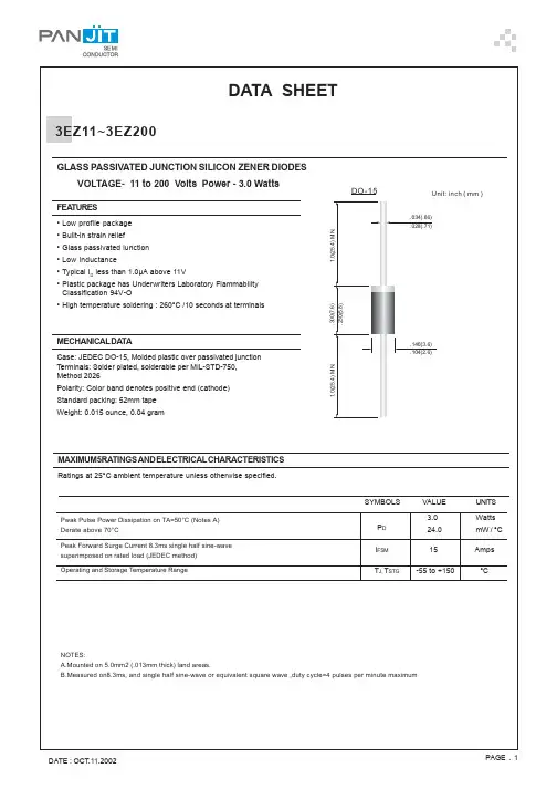
1SMB3EZ11 THRU 1SMB3EZ200SURFACE MOUNT SILICON ZENER DIODE VOLTAGE - 11 TO 200 Volts Power - 3.0 WattsFEA TURESl For surface mounted applications in order to optimize board space l Low profile package l Built-in strain reliefl Glass passivated junction l Low inductancel Excellent clamping capabilityl Typical I D less than 1£g A above 11V l High temperature soldering : 260¢J /10 seconds at terminalsl Plastic package has Underwriters Laboratory Flammability Classification 94V-O MECHANICAL DATACase: JEDEC DO-214AA, Molded plastic over passivated junctionTerminals: Solder plated, solderable per MIL-STD-750, method 2026Polarity: Color band denotes positive end (cathode) except BidirectionalStandard Packaging: 12mm tape(EIA-481)Weight: 0.003 ounce, 0.093 gramMAXIMUM RA TINGS AND ELECTRICAL CHARACTERISTICSRatings at 25¢J ambient temperature unless otherwise specified.SYMBOLVALUEUNITS Peak Pulse Power Dissipation (Note A)Derate above 75¢JP D 324Watts mW/¢J Peak forward Surge Current 8.3ms single half sine-wave superimposed on rated load(JEDEC Method) (Note B)I FSM 15Amps Operating Junction and Storage Temperature Range T J ,T STG -55 to +150¢JNOTES:A. Mounted on 5.0mm 2(.013mm thick) land areas.B. Measured on 8.3ms, single half sine-wave or equivalent square wave, duty cycle = 4 pulses per minute maximum.DO-214AA MODIFIED J-BEND1SMB3EZ11 THRU 1SMB3EZ200ELECTRICAL CHARACTERISTICS (T A=25¢J unless otherwise noted) V F=1.2 V max , I F=500 mA for all typesMaximum Zener Impedance(Note 3.)Leakage CurrentType No. (Note 1.)NominalZener VoltageVz @ I ZTvolts(Note 2.)T estcurrentI ZTmAZ ZT @ I ZTOhmsZ Zk @ I ZKOhmsI ZKmAI R£g A Max@V RVoltsMaximumZenerCurrentI ZMMadcSurgeCurrent@ T A = 25¢Jir - mA(Note 4.)DeviceMarkingCode1SMB3EZ11 1SMB3EZ12 1SMB3EZ1311121368635844.54.57007007000.250.250.25110.58.49.19.92252462081.821.661.5411B12B13B1SMB3EZ14 1SMB3EZ15 1SMB3EZ16 1SMB3EZ17141516175350474455.55.567007007007500.250.250.250.250.50.50.50.510.611.412.2131931801691501.431.331.251.1814B15B16B17B1SMB3EZ18 1SMB3EZ19 1SMB3EZ20 1SMB3EZ22181920224240373467787507507507500.250.250.250.250.50.50.50.513.714.415.216.71591421351231.111.0510.9118B19B20B22B1SMB3EZ24 1SMB3EZ27 1SMB3EZ28 1SMB3EZ302427283031282725910121675075075010000.250.250.250.250.50.50.50.518.220.62122.511210096900.830.740.710.6724B27B28B30B1SMB3EZ33 1SMB3EZ36 1SMB3EZ39 1SMB3EZ4333363943232119172022283310001000100015000.250.250.250.250.50.50.50.525.127.429.732.7827569630.610.560.510.4533B36B39B43B1SMB3EZ47 1SMB3EZ51 1SMB3EZ56 1SMB3EZ6247515662161513123845505515001500200020000.250.250.250.250.50.50.50.535.638.842.647.1575348440.420.390.360.3247B51B56B62B1SMB3EZ68 1SMB3EZ75 1SMB3EZ82 1SMB3EZ916875829111109.18.270859511520002000300030000.250.250.250.250.50.50.50.551.75662.269.2403633300.290.270.240.2268B75B82B91B1SMB3EZ100 1SMB3EZ110 1SMB3EZ120 1SMB3EZ1301001101201307.56.86.35.816022530037530004000450050000.250.250.250.250.50.50.50.57683.691.298.8272522210.20.180.160.15100B110B120B130B1SMB3EZ140 1SMB3EZ150 1SMB3EZ160 1SMB3EZ1701401501601705.354.74.447555062565050006000650070000.250.250.250.250.50.50.50.5106.4114121.6130.4191817160.140.130.120.12140B150B160B170B1SMB3EZ180 1SMB3EZ190 1SMB3EZ2001801902004.243.77008008757000800080000.250.250.250.50.50.5136.8144.81521514130.110.10.1180B190B200BNOTES:1. TOLERANCES - Suffix indicates 5% tolerance any other tolerance will be considered as a special device.2. ZENER VOLTAGE (Vz) MEASUREMENT - guarantees the zener voltage when measured at 40 ms¡Ó10ms from the diode body, and an ambient temperature of 25¢J(¡Ï8¢J, -2¢J).3.ZENER IMPEDANCE (Zz) DERIVATION - The zener impedance is derived from the 60 cycle ac voltage, which results when an ac current having an rms falue equal to 10% of the dc zener current (I ZT or I ZK) is superimposed on I ZT or I ZK.4. SURGE CURRENT (Ir) NON-REPETITIVE - The rating listed in the electrical characteristics table is maximum peak, non-repetitive, reverse surge current of 1/2 square wave or equivalent sine wave pulseof 1/120 second duration superimposed on the test current, I ZT, per JEDEC standards, however, actual device capability is as described in Figure 3.1SMB3EZ11 THRU 1SMB3EZ2000.00010.00020.00050.0010.0020.0050.010.020.050.10.20.512510Fig. 2-TYPICAL THERMAL RESPONSE L,P.W. PULSE WIDTH (ms)0.10.050.030.020.010.0050.0030.0020.0010.00050.00030.00020.0001 1251020501002005001KNOMINAL VZ (VOLTS)Fig. 3-MAXIMUM SURGE POWERFig. 4-TYPICAL REVERSE LEAKAGEVZ, ZENER VOLTAGE @IZT (VOLTS)VZ, ZENER VOLTAGE @IZT (VOLTS)Fig. 5-UNITS TO 12 VOLTS Fig. 6-UNITS 10 TO 200 VOLTS1SMB3EZ11 THRU 1SMB3EZ200VZ, ZENER VOLTAGE (VOLTS)VZ, ZENER VOLTAGE (VOLTS)Fig. 7-VZ = 3.9 THRU 10 VOLTS Fig. 8-VZ = 12 THRU 82 VOLTSVZ, ZENER VOLTAGE (VOLTS)L, LEAD LENGTH TO HEAT SINK (INCH)Fig. 9-VZ = 100 THRU 200 VOLTS Fig. 10-TYPICAL THERMAL RESISTANCEAPPLICATION NOTE:Since the actual voltage available from a given zener diode is temperature dependent, it is necessary to determine junction temperature under any set of operating conditions in order to calculate its value. The following procedure is recommended:Lead Temperature, T L, should be determined from:TL = £c LA P D + T A£c LA is the lead-to-ambient thermal resistance (¢J/W) and P D is the power dissipation. The value for £c LA will vary and depends on the device mounting method.£c LA is generally 30-40¢J/W for the various chips and tie points in common use and for printed circuit board wiring.The temperature of the lead can also be measured using a thermocouple placed on the lead as close as possible to the tie point. The thermal mass connected to the tie point is normally large enough so that it will not significantly respond to heat surges generated in the diode as a result of pulsed operation once steady-state conditions are achieved. Using the measured value of T L, the junction temperature may be determined by:T J = T L + £G T JL£G T JL is the increase in junction temperature above the lead temperature and may be found from Figure 2 for a train of power pulses or from Figure 10 for dc power.£G T JL = £c LA P DFor worst-case design, using expected limits of Iz, limits of P D and the extremes of T J (£G T JL ) may be estimated. Changes in voltage, Vz, can then be found from:£G V = £c VZ £G T J£c VZ , the zener voltage temperature coefficient, is found from Figures 5 and 6.Under high power-pulse operation, the zener voltage will vary with time and may also be affected significantly be the zener resistance. For best regulation, keep current excursions as low as possible.Data of Figure 2 should not be used to compute surge capability. Surge limitations are given in Figure 3. They are lower than would be expected by considering only junction temperature, as current crowding effects cause temperatures to be extremely high in small spots resulting in device degradation should the limits of Figure 3 be exceeded.。