
742841210;中文规格书,Datasheet资料
- 格式:pdf
- 大小:1.12 MB
- 文档页数:7


MB10S — Bridge Rectifier
© 2010 Fairchild Semiconductor Corporation
MB10S Rev. A01 July 2010
MB10S
Bridge Rectifier
Features
•Low leakage
•Surge overload rating : 35 amperes peak.
•Ideal for printed circuit board.
•UL certified, UL #E111753 and E326243.
Absolute Maximum Ratings * T
A = 25°C unless otherwise noted
* These ratings are limiting values above which the serviceability of any semiconductor device may by impaired.
Thermal Characteristics
* Device mounted on PCB with 0.5" x 0.5" (13 x 13 mm) lead length
Electrical Characteristics T
A = 25°C unless otherwise notedSymbolParameterValueUnits
V
RRMMaximum Repetitive Reverse Voltage1000V
V
RMSMaximum RMS Bridge Input Voltage700V
V
RDC Reverse Voltage (Rated V
R)1000V
I
F(AV)Average Rectified Forward Current, @ T
A = 50°C
On Glass-epoxy P.C.B.
On Aluminum substrate0.5
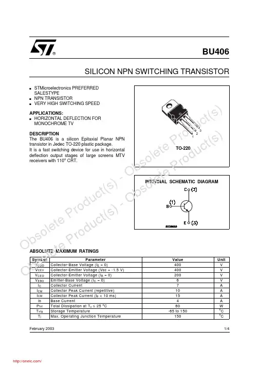
BU406SILICON NPN SWITCHING TRANSISTORsSTMicroelectronics PREFERREDSALESTYPE sNPN TRANSISTOR sVERY HIGH SWITCHING SPEED APPLICATIONS: sHORIZONTAL DEFLECTION FORMONOCHROME TV DESCRIPTION The BU406 is a silicon Epitaxial Planar NPNtransistor in Jedec TO-220 plastic package.It is a fast switching device for use in horizontaldeflection output stages of large screens MTVreceivers with 110o
CRT.®INTERNAL SCHEMATIC DIAGRAMFebruary 2003 123TO-220
ABSOLUTE MAXIMUM RATINGSSymbolParameterValueUnitVCBOCollector-Base Voltage (IE = 0)400VVCEVCollector-Emitter Voltage (VBE = -1.5 V)400VVCEOCollector-Emitter Voltage (IB = 0)200VVEBOEmitter-Base Voltage (IC = 0)6VICCollector Current7AICMCollector Peak Current (repetitive)10AICMCollector Peak Current (tp < 10 ms)15AIBBase Current4APtotTotal Dissipation at Tc ≤ 25 oC60WTstgStorage Temperature-65 to 150oCTjMax. Operating Junction Temperature150oC1/4Obsolete Product(s) - Obsolete Product(s)

SymbolVDSVGSIDMTJ, TSTGSymbolTypMax360415400460RθJL300350Maximum Junction-to-Lead CSteady-State°C/WThermal CharacteristicsParameterUnitsMaximum Junction-to-Ambient At ≤ 10sRθJA°C/WMaximum Junction-to-Ambient ASteady-State°C/WWTA=70°C0.19Junction and Storage Temperature Range-55 to 150°CPower Dissipation ATA=25°CPD0.3ATA=70°C0.7Pulsed Drain Current B5Continuous Drain Current ATA=25°CID0.9Drain-Source Voltage20VGate-Source Voltage±8VAbsolute Maximum Ratings TA=25°C unless otherwise notedParameterMaximumUnitsAO7800Dual N-Channel Enhancement Mode Field Effect TransistorFeaturesVDS (V) = 20VID = 0.9 A (VGS = 4.5V)RDS(ON) < 300mΩ (VGS = 4.5V)RDS(ON) < 350mΩ (VGS = 2.5V)RDS(ON) < 450mΩ (VGS = 1.8V)General DescriptionThe AO7800 uses advanced trench technology to provide excellent RDS(ON), low gate charge and operation with gate voltages as low as 1.8V, in the small SOT323 footprint. It can be used for a wide variety of applications, including load switching, low current inverters and low current DC-DC converters.It is ESD protected. Standard Product AO7800 is Pb-free (meets ROHS & Sony 259 specifications). AO7800L is a Green Product ordering option. AO7800 and AO7800L are electrically identical.SC-70-6(SOT-323)Top ViewD1

E-mail: info@Page 1 of 2©2009 by RF Monolithics, Inc.
RO3104 - 2/4/09Electrical Characteristics CharacteristicSymNotesMinimumTypicalMaximumUnitsCenter Frequency (+25 °C)Absolute FrequencyfC2, 3, 4, 5303.750303.900MHzTolerance from 303.825 MHz∆fC±75kHzInsertion LossIL2, 5, 61.32.0dBQuality FactorUnloaded QQU5, 6, 71300050 Ω Loaded QQL1700Temperature StabilityTurnover Temperature
TO6, 7, 810
2540°CTurnover Frequency
fOfc Frequency Temperature CoefficientFTC0.037ppm/°C2Frequency AgingAbsolute Value during the First Year|fA|1≤10ppm/yrDC Insulation Resistance between Any Two Pins51.0MΩRF Equivalent RLC ModelMotional ResistanceRM5, 7, 915ΩMotional InductanceLM103µHMotional CapacitanceCM2.6fFPin 1 to Pin 2 Static CapacitanceCO5, 6, 92.3pFTransducer Static CapacitanceCP5, 6, 7, 92.0pFTest Fixture Shunt InductanceLTEST2, 7122nHLid Symbolization (in Addition to Lot and/or Date Codes)RFM RO3104