DAC121S101WGRQV中文资料
- 格式:pdf
- 大小:459.71 KB
- 文档页数:22
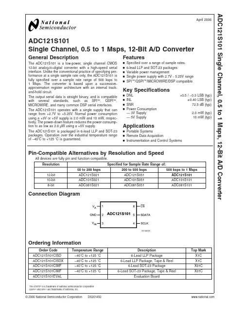
August 14, 2008 DAC121S101QML12-Bit Micro Power Digital-to-Analog Converter with Rail-to-Rail OutputGeneral DescriptionThe DAC121S101 is a full-featured, general purpose 12-bit voltage-output digital-to-analog converter (DAC) that can op-erate from a single +2.7 V to 5.5 V supply and consumes just 177 µA of current at 3.6 V. The on-chip output amplifier allows rail-to-rail output swing and the three wire serial interface op-erates at clock rates up to 20 MHz over the specified supply voltage range and is compatible with standard SPI™, QSPI, MICROWIRE and DSP interfaces.The supply voltage for the DAC121S101 serves as its voltage reference, providing the widest possible output dynamic range. A power-on reset circuit ensures that the DAC output powers up to zero volts and remains there until there is a valid write to the device. A power-down feature reduces power consumption to less than a microWatt.The low power consumption and small packages of the DAC121S101 make it an excellent choice for use in battery operated equipment.The DAC121S101 operates over the extended temperature range of -55°C to +125°C.Features■Guaranteed Monotonicity■Low Power Operation■Rail-to-Rail Voltage Output■Power-on Reset to Zero Volts Output■SYNC Interrupt Facility■Wide power supply range (+2.7 V to +5.5 V)■Small Packages■Power Down FeatureKey Specifications■Resolution12 bits ■DNL+0.21, -0.10 LSB (typ)■Output Settling Time12.5 µs (typ)■Zero Code Error 2.1 mV (typ)■Full-Scale Error−0.04 %FS (typ)■Power Dissipation—Normal Mode0.52 mW (3.6 V) / 1.19 mW (5.5 V) typ —Pwr DownMode0.014 µW (3.6 V) / 0.033 µW (5.5 V) typ ■Total Ionizing Dose100 krad(Si)■Single Event Latch-up120 MeV-cm2/mg Applications■Battery-Powered Instruments■Digital Gain and Offset Adjustment■Programmable Voltage & Current Sources■Programmable AttenuatorsOrdering InformationNS PART NUMBER SMD PART NUMBER NS PACKAGE NUMBER PACKAGE DISCRIPTION DAC121S101WGMLS WG10A10LD Ceramic SOICDAC121S101WGRQV(Note 11)TBD WG10A10LD Ceramic SOICSPI™ is a trademark of Motorola, Inc.© 2008 National Semiconductor DAC121S101QML 12-Bit Micro Power Digital-to-Analog Converter with Rail-to-Rail OutputConnection Diagrams10LD Ceramic SOIC30018001Top ViewSee NS Package Number WG10ABlock Diagram30018003 2D A C 121S 101Q M LAbsolute Maximum Ratings(Notes 1, 2)Supply Voltage, VA6.5 VVoltage on any Input Pin−0.3 V to (VA+ 0.3 V) Input Current at Any Pin (Note 3)10 mA Maximum Output Current (Note 10)10 mAVOUTPin in Powerdown Mode 1.0 mA Package Input Current (Note 3)20 mAPower Dissipation at TA= 25°C See (Note 4) Maximum Junction Temperature175°C Lead TemperatureCeramic SOIC(Soldering 10 Seconds)260°C Storage Temperature−65°C to +150°C Package Weight (Typical)Ceramic SOIC220 mg ESD Tolerance (Note 5)Class 3A (5000 V)Operating Ratings (Notes 1, 2)Operating Temperature Range−55°C to +125°C Supply Voltage, VA+2.7 V to 5.5 VAny Input Voltage (Note 6)−0.1 V to (VA+ 0.1 V) Output Load0 to 1500 pF SCLK Frequency Up to 20 MHz Package Thermal ResistancePackageθJA(Still Air)θJC10-lead Ceramic SOICPackage on 2 layer, 1oz.PCB214°C/W25.7°C/WQuality Conformance InspectionMIL-STD-883, Method 5005 - Group ASubgroup Description Temp (° C)1Static tests at+252Static tests at+1253Static tests at-554Dynamic tests at+255Dynamic tests at+1256Dynamic tests at-557Functional tests at+258A Functional tests at+1258B Functional tests at-559Switching tests at+2510Switching tests at+12511Switching tests at-5512Setting time at+2513Setting time at+12514Setting time at-55DAC121S101QMLDAC121S101 Electrical Characteristics DC ParametersThe following specifications apply for V A = +2.7 V to +5.5 V, R L = ∞, C L = 200 pF to GND, f SCLK = 20 MHz, input code range 48 to 4047. Boldface limits apply for T MIN ≤ T A ≤ T MAX : all other limits T A = 25°C, unless otherwise specified.SymbolParameterConditionsNotesTypical (Note 8)MinMaxUnitsSub-groupsSTATIC PERFORMANCEResolution (Note 9) 12 Bits Monotonicity(Note 9) 12 Bits INL Integral Non-Linearity Over Decimal codes 48 to 4047 ±2.75−8.08.0LSB 1, 2, 3DNL Differential Non-Linearity V A = 2.7 V to 5.5 V +0.21 +1.0LSB 1, 2, 3−0.10−0.7 LSB 1, 2, 3ZE Zero Code Error I OUT = 0 +2.12 +15mV 1, 2, 3FSE Full-Scale Error I OUT = 0−0.04 −1.0%FSR 1, 2, 3GE Gain ErrorAll ones Loaded to DAC register −0.11 ±1.0%FSR 1, 2, 3ZCED Zero Code Error Drift (Note 9)−20µV/°C TC GEGain Error TempcoV A = 3 V (Note 9)−0.7 ppm/°C V A = 5 V−1.0ppm/°COUTPUT CHARACTERISTICSIPD SINKVout Pin in Powerdown ModeAll PD Modes (Note 9) 1.0mAOutput Voltage Range(Note 9) 0V A V ZCO Zero Code OutputV A = 3 V, I OUT = 10 µA2.0 6mV 1, 2, 3V A = 3 V, I OUT = 100 µA 4 10mV 1, 2, 3V A = 5 V, I OUT = 10 µA 2 8mV 1, 2, 3V A = 5 V, I OUT = 100 µA 4 9mV 1, 2, 3FSO Full Scale OutputV A = 3 V, I OUT = 10 µA 2.997 2.990 V 1, 2, 3V A = 3 V, I OUT = 100 µA 2.991 2.985 V 1, 2, 3V A = 5 V, I OUT = 10 µA 4.994 4.985 V 1, 2, 3V A = 5 V, I OUT = 100 µA 4.992 4.985 V 1, 2, 3 Maximum Load CapacitanceR L = ∞(Note 9)1500 pF R L = 2 k Ω1500 pFDC Output Impedance816Ω1, 2, 3 4D A C 121S 101Q M LDC Parameters (Continued)The following specifications apply for V A = +2.7 V to +5.5 V, R L = ∞, C L = 200 pF to GND, f SCLK = 20 MHz, input code range 48 to 4047. Boldface limits apply for T MIN ≤ T A ≤ T MAX : all other limits T A = 25°C, unless otherwise specified.Symbol ParameterConditionsNotesTypical (Note 8)MinMaxUnitsSub-groupsLOGIC INPUTI IN Input Current 6−200+200nA 1, 2, 3V IL Input Low Voltage V A = 5 V0.8V 1, 2, 3V A = 3 V0.5V 1, 2, 3V IH Input High Voltage V A = 5 V 2.4 V 1, 2, 3V A = 3 V 2.1 V 1, 2, 3C INInput Capacitance(Note 9)5pFPOWER REQUIREMENTSI ASupply Current (output unloaded)Normal Mode f SCLK = 20 MHz 5.5 V 216 270µA 1, 2, 33.6 V 145 200µA 1, 2, 3Normal Mode f SCLK = 10 MHz5.5 V 185 230µA 1, 2, 33.6 V 132 175µA 1, 2, 3Normal Mode f SCLK = 0 5.5 V 150 190µA 1, 2, 33.6 V 115 160µA 1, 2, 3All PD Modes,f SCLK = 20 MHz 5.5 V 22 60µA 1, 2, 33.6 V 12 30µA 1, 2, 3All PD Modes,f SCLK = 10 MHz 5.5 V 12 40µA 1, 2, 33.6 V 6 20µA 1, 2, 3All PD Modes,f SCLK = 0 5.5 V .006 1.0µA 1, 2, 33.6 V .004 1.0µA 1, 2, 3P CPower Consumption (output unloaded)Normal Mode f SCLK = 20 MHz 5.5 V (Note 9) 1.19 1.49mW 3.6 V 0.52 .72mW Normal Mode f SCLK = 10 MHz5.5 V (Note 9) 1.02 1.27mW 3.6 V 0.47 .63mW Normal Modef SCLK = 0 5.5 V (Note 9)0.82 1.05mW 3.6 V 0.41 .58mW All PD Modes,f SCLK = 20 MHz 5.5 V (Note 9)0.12 .33mW 3.6 V 0.07 .11mW All PD Modes,f SCLK = 10 MHz 5.5 V (Note 9)0.04 .22mW 3.6 V 0.02 .08mW All PD Modes,f SCLK = 05.5 V (Note 9)0.033 5.5µW 3.6 V0.014 3.6µW I OUT / I APower EfficiencyI LOAD = 2 mA(Note 9)91 % 94%DAC121S101QMLAC and Timing CharacteristicsThe following specifications apply for V A = +2.7 V to +5.5 V, R L = ∞, C L = 200 pF to GND, f SCLK = 20 MHz, input code range 48 to 4047. Boldface limits apply for T MIN ≤ T A ≤ T MAX : all other limits T A = 25°C, unless otherwise specified.Symbol ParameterConductionsNotes Typical (Note 8)Min Max Units Sub-groupsf SCLKSCLK Frequency(Note 9) 20MHz t sOutput Voltage Settling TimeFF0 to 00F codechange, R L = ∞C L ≤ 200 pF12.5 15µs 9, 10, 11C L = 500 pF12.5 15µs 9, 10, 1100Fh to FF0h code change, R L = ∞C L ≤ 200 pF 12.5 15µs 9, 10, 11C L = 500 pF12.5 15µs 9, 10, 11SR Output Slew Rate(Note 9)1 V/µs Glitch Impulse Code change from 800h to 7FFh (Note 9)12 nV-sec Digital Feedthrough (Note 9)0.5 nV-sec t WU Wake-Up Time V A = 5 V (Note 9).65 µs V A = 3 V 1.1 µs 1/f SCLK SCLK Cycle Time 50 ns 9, 10, 11t H SCLK High time 10 20ns 9, 10, 11t L SCLK Low Time10 20ns 9, 10, 11t SUCL Set-up Time SYNC to SCLKRising Edge−18−21 ns 9, 10, 11t SUD Data Set-Up Time 5 6ns 9, 10, 11t DHD Data Hold Time3 4.5ns 9, 10, 11t CS SCLK fall to rise of SYNC V A = 5.5 V 6 10ns 9, 10, 11V A = 2.7 V 11 18ns 9, 10, 11t SYNCSYNC High TimeV A = 5.5 V 33 37ns 9, 10, 11V A = 2.7 V3436ns9, 10, 11 6D A C 121S 101Q M LRadiation Electrical Characteristics (Note 11)The following specifications apply for VA = +2.7 V to +5.5 V, RL= ∞, C L = 200 pF to GND, f SCLK = 20 MHz, input code range 48 to4047.Symbol Parameter Conditions Notes Typical(Note 8)Min Max UnitsSub-groupsPOWER REQUIREMENTSI A Supply Current (outputunloaded)Normal ModefSCLK= 20 MHz5.5 V216325µA13.6 V145250µA1Normal ModefSCLK= 10 MHz5.5 V185300µA13.6 V132225µA1Normal ModefSCLK= 05.5 V150275µA13.6 V115200µA1All PD Modes,fSCLK= 20 MHz5.5 V22125µA13.6 V12100µA1All PD Modes,fSCLK= 10 MHz5.5 V12115µA13.6 V695µA1All PD Modes,fSCLK= 05.5 V.006100µA13.6 V.004100µA1Note 1:Absolute Maximum Ratings indicate limits beyond which damage to the device may occur. Operating Ratings indicate conditions for which the device is functional, but do not guarantee specific performance limits. For guaranteed specifications and test conditions, see the Electrical Characteristics. The guaranteed specifications apply only for the test conditions listed. Some performance characteristics may degrade when the device is not operated under the listed test conditions.Note 2:All voltages are measured with respect to GND = 0 V, unless otherwise specifiedNote 3:When the input voltage at any pin exceeds the power supplies (that is, less than GND, or greater than VA ), the current at that pin should be limited to 10mA. The 20 mA maximum package input current rating limits the number of pins that can safely exceed the power supplies with an input current of 10 mA to two.Note 4:The absolute maximum junction temperature (TJ max) for this device is 175°C. The maximum allowable power dissipation is dictated by TJmax, thejunction-to-ambient thermal resistance (θJA ), and the ambient temperature (TA), and can be calculated using the formula PDMAX = (TJmax − TA) / θJA. The valuesfor maximum power dissipation will be reached only when the device is operated in a severe fault condition (e.g., when input or output pins are driven beyond the power supply voltages, or the power supply polarity is reversed). Obviously, such conditions should always be avoided.Note 5:Human body model is 100 pF capacitor discharged through a 1.5 kΩ resistor. Machine model is 220 pF discharged through ZERO Ohms.Note 6:The analog inputs are protected as shown below. Input voltage magnitudes up to VA + 300 mV or to 300 mV below GND will not damage this device.However, errors in the conversion result can occur if any input goes above VA or below GND by more than 100 mV. For example, if VAis 2.7 VDC, ensure that−100 mV ≤ input voltages ≤2.8 V DC to ensure accurate conversions.30018004Note 7:To guarantee accuracy, it is required that VAbe well bypassed.Note 8:Typical figures are at TJ= 25°C, and represent most likely parametric norms.Note 9:This parameter is guaranteed by design and/or characterization and is not tested in production.Note 10:Maximum Output Current may not exceed 10 mA. At VDD = 5.5 V the minimum external resistive load can be no less than 550 Ω, (360 Ω at VDD= 3.6V).Note 11:Pre and post irradiation limits are identical to those listed in the “DC Parameters” and “AC and Timing Characteristics” tables, except as listed in the “Radiation Electrical Characteristics” table. When performing post irradiation electrical measurements for any RHA level, TA= +25°C. DAC121S101QMLSpecification DefinitionsDIFFERENTIAL NON-LINEARITY (DNL) is the measure of the maximum deviation from the ideal step size of 1 LSB,which is V REF / 4096 = V A / 4096.DIGITAL FEEDTHROUGH is a measure of the energy inject-ed into the analog output of the DAC from the digital inputs when the DAC outputs are not updated. It is measured with a full-scale code change on the data bus.FULL-SCALE ERROR is the difference between the actual output voltage with a full scale code (FFFh) loaded into the DAC and the value of V A x 4095 / 4096.GAIN ERROR is the deviation from the ideal slope of the transfer function. It can be calculated from Zero and Full-Scale Errors as GE = FSE - ZE, where GE is Gain error, FSE is Full-Scale Error and ZE is Zero Error.GLITCH IMPULSE is the energy injected into the analog out-put when the input code to the DAC register changes. It is specified as the area of the glitch in nanovolt-seconds.INTEGRAL NON-LINEARITY (INL) is a measure of the de-viation of each individual code from a straight line through the input to output transfer function. The deviation of any given code from this straight line is measured from the center of that code value. The end point method is used. INL for this product is specified over a limited range, per the Electrical Tables.LEAST SIGNIFICANT BIT (LSB) is the bit that has the small-est value or weight of all bits in a word. This value isLSB = V REF / 2nwhere V REF is the supply voltage for this product, and "n" is the DAC resolution in bits, which is 12 for the DAC121S101.MAXIMUM LOAD CAPACITANCE is the maximum capaci-tance that can be driven by the DAC with output stability maintained.MONOTONICITY is the condition of being monotonic, where the DAC has an output that never decreases when the input code increases.MOST SIGNIFICANT BIT (MSB) is the bit that has the largest value or weight of all bits in a word. Its value is 1/2 of V A .POWER EFFICIENCY is the ratio of the output current to the total supply current. The output current comes from the power supply. The difference between the supply and output cur-rents is the power consumed by the device without a load.SETTLING TIME is the time for the output to settle to within 1/2 LSB of the final value after the input code is updated.WAKE-UP TIME is the time for the output to exit power-down mode. This is the time measured from the falling edge of 16th SCLK pulse to when the output voltage deviates from the power-down voltage of 0 V.ZERO CODE ERROR is the output error, or voltage, present at the DAC output after a code of 000h has been entered. 8D A C 121S 101Q M LTransfer Characteristic30018005FIGURE 1. Input / Output Transfer CharacteristicTiming Diagram30018006FIGURE 2. DAC121S101 Timing DAC121S101QMLTypical Performance Characteristicsf SCLK = 20 MHz, T A = 25C, Input Code Range 48 to 4047, unlessotherwise statedDNL at V A = 2.7V30018052DNL at V A = 5.5V30018053INL at V A = 2.7V 30018054INL at V A = 5.5V30018055DNL vs. V A 30018022INL vs. V A30018023 10D A C 121S 101Q M L2.7V DNL vs. f SCLK30018050 5.5V DNL vs. f SCLK300180512.7V DNL vs. Clock Duty Cycle 30018056 5.5V DNL vs. Clock Duty Cycle300180572.7V DNL vs. Temperature 30018026 5.5V DNL vs. Temperature30018027DAC121S101QML2.7V INL vs. f SCLK30018028 5.5V INL vs. f SCLK300180292.7V INL vs. Clock Duty Cycle 30018030 5.5V INL vs. Clock Duty Cycle300180312.7V INL vs. Temperature 30018032 5.5V INL vs. Temperature30018033 12D A C 121S 101Q M LZero Code Error vs. fSCLK30018034Zero Code Error vs. Temperature30018036Full-Scale Error vs. fSCLK30018037Full-Scale Error vs. Temperature30018039Supply Current vs. VA30018044Supply Current vs. Temperature30018045DAC121S101QML5V Glitch Response30018046Power-On Reset300180473V Wake-Up Time 300180485V Wake-Up Time30018049 14D A C 121S 101Q M L1.0 Functional Description1.1 DAC SECTIONThe DAC121S101 is fabricated on a CMOS process with an architecture that consists of switches and a resistor string that are followed by an output buffer. The power supply serves as the reference voltage. The input coding is straight binary with an ideal output voltage of:V OUT = V A x (D / 4096)where D is the decimal equivalent of the binary code that is loaded into the DAC register and can take on any value be-tween 0 and 4095.1.2 RESISTOR STRINGThe simplified resistor string is shown in Figure 3. Conceptu-ally, this string consists of 4096 equal valued resistors with a switch at each junction of two resistors, plus a switch to ground. The code loaded into the DAC register determines which switch is closed, connecting the proper node to the amplifier. This configuration guarantees that the DAC is monotonic.30018007FIGURE 3. DAC Resistor String1.3 OUTPUT AMPLIFIERThe output buffer amplifier is a rail-to-rail type, providing an output voltage range of 0V to V A . All amplifiers, even rail-to-rail types, exhibit a loss of linearity as the output approaches the supply rails (0V and V A , in this case). For this reason,linearity is specified over less than the full output range of the DAC. The output capabilities of the amplifier are described in the Electrical Tables.1.4 SERIAL INTERFACEThe three-wire interface is compatible with SPI, QSPI and MICROWIRE, as well as most DSPs. See the Timing Diagram for information on a write sequence.A write sequence begins by bringing the SYNC line low. Once SYNC is low, the data on the D IN line is clocked into the 16-bit serial input register on the falling edges of SCLK. On the 16th falling clock edge, the last data bit is clocked in and the programmed function (a change in the mode of operation and/or a change in the DAC register contents) is executed. At this point the SYNC line may be kept low or brought high. In eithercase, it must be brought high for the minimum specified time before the next write sequence as a falling edge of SYNC can initiate the next write cycle.Since the SYNC and D IN buffers draw more current when they are high, they should be idled low between write sequences to minimize power consumption.1.5 INPUT SHIFT REGISTERThe input shift register, Figure 4, has sixteen bits. The first two bits are "don't cares" and are followed by two bits that determine the mode of operation (normal mode or one of three power-down modes). The contents of the serial input register are transferred to the DAC register on the sixteenth falling edge of SCLK. See Timing Diagram, Figure 2.30018008FIGURE 4. Input Register ContentsNormally, the SYNC line is kept low for at least 16 falling edges of SCLK and the DAC is updated on the 16th SCLK falling edge. However, if SYNC is brought high before the 16th falling edge, the shift register is reset and the write sequence is invalid. The DAC register is not updated and there is no change in the mode of operation or in the output voltage.1.6 POWER-ON RESETThe power-on reset circuit controls the output voltage during power-up. Upon application of power the DAC register is filled with zeros and the output voltage is 0 Volts and remains there until a valid write sequence is made to the DAC.1.7 POWER-DOWN MODESThe DAC121S101 has four modes of operation. These modes are set with two bits (DB13 and DB12) in the control register.TABLE 1. Modes of OperationDB13DB12 Operating Mode 00Normal Operation01Power-Down with 5k Ω to GND 10Power-Down with 100k Ω to GND 11Power-Down with Hi-ZWhen both DB13 and DB12 are 0, the device operates nor-mally. For the other three possible combinations of these bits the supply current drops to its power-down level and the out-put is pulled down with either a 5k Ω or a 100k Ω resistor, or is in a high impedance state, as described in Table 1.The bias generator, output amplifier, the resistor string and other linear circuitry are all shut down in any of the power-down modes. However, the contents of the DAC register are unaffected when in power-down, so when coming out of pow-er down the output voltage returns to the same voltage it was before entering power down. Minimum power consumption is achieved in the power-down mode with SCLK disabled and SYNC and D IN idled low.15DAC121S101QML2.0 Applications InformationThe simplicity of the DAC121S101 implies ease of use. How-ever, it is important to recognize that any data converter thatutilizes its supply voltage as its reference voltage will haveessentially zero PSRR (Power Supply Rejection Ratio).Therefore, it is necessary to provide a noise-free supply volt-age to the device.2.1 DSP/MICROPROCESSOR INTERFACINGInterfacing the DAC121S101 to microprocessors and DSPsis quite simple. The following guidelines are offered to hastenthe design process.2.1.1 ADSP-2101/ADSP2103 InterfacingFigure 5 shows a serial interface between the DAC121S101and the ADSP-2101/ADSP2103. The DSP should be set tooperate in the SPORT Transmit Alternate Framing Mode. It isprogrammed through the SPORT control register and shouldbe configured for Internal Clock Operation, Active Low Fram-ing and 16-bit Word Length. Transmission is started by writinga word to the Tx register after the SPORT mode has beenenabled.30018009FIGURE 5. ADSP-2101/2103 Interface2.1.2 80C51/80L51 InterfaceA serial interface between the DAC121S101 and the80C51/80L51 microcontroller is shown in Figure 6. TheSYNC signal comes from a bit-programmable pin on the mi-crocontroller. The example shown here uses port line P3.3.This line is taken low when data is to transmitted to theDAC121S101. Since the 80C51/80L51 transmits 8-bit bytes,only eight falling clock edges occur in the transmit cycle. Toload data into the DAC, the P3.3 line must be left low after thefirst eight bits are transmitted. A second write cycle is initiatedto transmit the second byte of data, after which port line P3.3is brought high. The 80C51/80L51 transmit routine must rec-ognize that the 80C51/80L51 transmits data with the LSB firstwhile the DAC121S101 requires data with the MSB first.30018010FIGURE 6. 80C51/80L51 Interface2.1.3 68HC11 InterfaceA serial interface between the DAC121S101 and the 68HC11microcontroller is shown in Figure 7. The SYNC line of theDAC121S101 is driven from a port line (PC7 in the figure),similar to the 80C51/80L51.The 68HC11 should be configured with its CPOL bit as a zeroand its CPHA bit as a one. This configuration causes data onthe MOSI output to be valid on the falling edge of SCLK. PC7is taken low to transmit data to the DAC. The 68HC11 trans-mits data in 8-bit bytes with eight falling clock edges. Data istransmitted with the MSB first. PC7 must remain low after thefirst eight bits are transferred. A second write cycle is initiatedto transmit the second byte of data to the DAC, after whichPC7 should be raised to end the write sequence.30018011FIGURE 7. 68HC11 Interface2.1.4 Microwire InterfaceFigure 8 shows an interface between a Microwire compatibledevice and the DAC121S101. Data is clocked out on the risingedges of the SCLK signal.30018012FIGURE 8. Microwire Interface2.2 USING REFERENCES AS POWER SUPPLIESRecall the need for a quiet supply source for devices that usetheir power supply voltage as a reference voltage.Since the DAC121S101 consumes very little power, a refer-ence source may be used as the supply voltage. The advan-tages of using a reference source over a voltage regulator areaccuracy and stability. Some low noise regulators can also beused for the power supply of the DAC121S101. Listed beloware a few power supply options for the DAC121S101.2.2.1 LM4130The LM4130 reference, with its 0.05% accuracy over tem-perature, is a good choice as a power source for theDAC121S101. Its primary disadvantage is the lack of 3 V and5 V versions. However, the 4.096 V version is useful if a 0 to4.095 V output range is desirable or acceptable. Bypassingthe LM4130 VIN pin with a 0.1 µF capacitor and the VOUTpin with a 2.2 µF capacitor will improve stability and reduceoutput noise. The LM4130 comes in a space-saving 5-pinSOT23.30018013FIGURE 9. The LM4130 as a power supply 16DAC121S11QML2.2.2 LM4050Available with accuracy of 0.44%, the LM4050 shunt refer-ence is also a good choice as a power regulator for the DAC121S101. It does not come in a 3 Volt version, but 4.096V and 5 V versions are available. It comes in a space-saving 3-pin SOT23.30018014FIGURE 10. The LM4050 as a power supplyThe minimum resistor value in the circuit of Figure 10 should be chosen such that the maximum current through the LM4050 does not exceed its 15 mA rating. The conditions for maximum current include the input voltage at its maximum,the LM4050 voltage at its minimum, the resistor value at its minimum due to tolerance, and the DAC121S101 draws zero current. The maximum resistor value must allow the LM4050to draw more than its minimum current for regulation plus the maximum DAC121S101 current in full operation. The condi-tions for minimum current include the input voltage at its minimum, the LM4050 voltage at its maximum, the resistor value at its maximum due to tolerance, and the DAC121S101draws its maximum current. These conditions can be sum-marized asR(min) = ( V IN (max) − V Z (min) / (I A (min) + I Z (max))andR(max) = ( V IN (min) − V Z (max) / (I A (max) + I Z (min) )where V Z (min) and V Z (max) are the nominal LM4050 output voltages ± the LM4050 output tolerance over temperature, I Z (max) is the maximum allowable current through the LM4050,I Z (min) is the minimum current required by the LM4050 for proper regulation, I A (max) is the maximum DAC121S101 sup-ply current, and I A (min) is the minimum DAC121S101 supply current.2.2.3 LP3985The LP3985 is a low noise, ultra low dropout voltage regulator with a 3% accuracy over temperature. It is a good choice for applications that do not require a precision reference for the DAC121S101. It comes in 3.0V, 3.3V and 5V versions, among others, and sports a low 30 µV noise specification at low fre-quencies. Since low frequency noise is relatively difficult to filter, this specification could be important for some applica-tions. The LP3985 comes in a space-saving 5-pin SOT23 and 5-bump micro SMD packages.30018015FIGURE 11. Using the LP3985 regulatorAn input capacitance of 1.0µF without any ESR requirement is required at the LP3985 input, while a 1.0µF ceramic ca-pacitor with an ESR requirement of 5m Ω to 500m Ω is required at the output. Careful interpretation and understanding of the capacitor specification is required to ensure correct device operation.2.2.4 LP2980The LP2980 is an ultra low dropout regulator with a 0.5% or 1.0% accuracy over temperature, depending upon grade. It is available in 3.0V, 3.3V and 5V versions, among others.30018016FIGURE 12. Using the LP2980 regulatorLike any low dropout regulator, the LP2980 requires an output capacitor for loop stability. This output capacitor must be at least 1.0µF over temperature, but values of 2.2µF or more will provide even better performance. The ESR of this capacitor should be within the range specified in the LP2980 data sheet.Surface-mount solid tantalum capacitors offer a good combi-nation of small size and ESR. Ceramic capacitors are attrac-tive due to their small size but generally have ESR values that are too low for use with the LP2980. Aluminum electrolytic capacitors are typically not a good choice due to their large size and have ESR values that may be too high at low tem-peratures.2.3 BIPOLAR OPERATIONThe DAC121S101 is designed for single supply operation and thus has a unipolar output. However, a bipolar output may be obtained with the circuit in Figure 13. This circuit will provide an output voltage range of ±5 Volts. A rail-to-rail amplifier should be used if the amplifier supplies are limited to ±5V.DAC121S101QML。