MURATA 通用电容选型参考
- 格式:pdf
- 大小:288.57 KB
- 文档页数:10
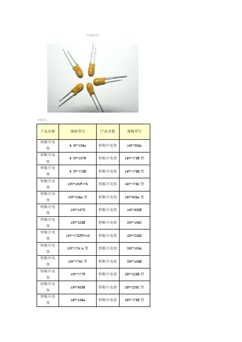
钽电解电容详细信息:固体钽电容器是1956年由美国贝乐试验室首先研制成功的,它的性能优异,是所有电容器中体积小而又能达到较大电容量的产品。
钽电容器外形多种多样,并容易制成适于表面贴装的小型和片型元件。
适应了目前电子技术自动化和小型化发展的需要。
虽然钽原料稀缺,钽电容价格较昂贵,但由于大量采用高比容钽粉(30KuF.g-100KuF.V/g),加上对电容器制造工艺的改进和完善,钽电解电容器还是得到了迅速的发展,使用范围日益广泛。
钽电容器不仅在军事通讯,航天等领域广泛使用,而且使用范围还在向工业控制,影视设备、通讯仪表等产品中大量使用。
目前生产的钽电解电容器主要有烧结型固体、箔形卷绕固体、烧结型液体等三种,其中烧结型固体约占目前生产总量的95%以上,而又以非金属密封型的树脂封装式为主体。
小型化、片式化配合SMT技术下方兴未艾,片式烧结钽电容器已逐渐成主流。
固体钽电容器电性能优良,工作温度范围宽,而且形式多样,体积效率优异,具有其独特的特征:钽电解电容器的工作介质是在钽金属表面生成的一层极薄的五氧化二钽膜。
此层氧化膜介质完全与组成电容器的一端极结合成一个整体,不能单独存在。
因此单位体积内所具有的电容量特别大。
即比容量非常高,因此特别适宜于小型化。
在钽电解电容器工作过程中,具有自动修补或隔绝氧化膜中的疵点所在的性能,使氧化膜介质随时得到加固和恢复其应有的绝缘能力,而不致遭到连续的累积性破坏。
这种独特自愈性能,保证了其长寿命和可靠性的优势。
钽电解电容器具有非常高的工作电场强度,并较任何类型电容器都大,以此保证它的小型化。
钽电解电容器可以非常方便地获得较大的电容量,在电源滤波、交流旁路等用途上少有竞争对手。
具有单向导电性,即所谓有“极性”,应用时应按电源的正、负方向接入电流,电容器的阳极(正极)接电源“+”极,阴极(负极)接电源的“-”极;如果接错不仅电容器发挥不了作用,而且漏电流很大,短时间内芯子就会发热,破坏氧化膜随即失效。
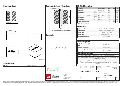
Dimensions: [mm]Scale - 8:1Product Marking:Marking2R2 (Inductance Code)744383360227443833602274438336022B C(mm)B(mm) min.178,001,507443833602274438336022T e m p e r a t u r eT pT L74438336022Cautions and Warnings:The following conditions apply to all goods within the product series of WE-MAPI ofWürth Elektronik eiSos GmbH & Co. KG:General:•This electronic component was designed and manufactured for use in general electronic equipment.•Würth Elektronik must be asked for written approval (following the PPAP procedure) before incorporating the components into any equipment in fields such as military, aerospace, aviation, nuclear control, submarine, transportation (automotive control, train control, ship control), transportation signal, disaster prevention, medical, public information network, etc. where higher safety and reliability are especially required and/or if there is the possibility of direct damage or human injury.•Electronic components that will be used in safety-critical or high-reliability applications, should be pre-evaluated by the customer. •The component is designed and manufactured to be used within the datasheet specified values. If the usage and operation conditions specified in the datasheet are not met, the wire insulation may be damaged or dissolved.•Do not drop or impact the components, the component may be damaged.•Würth Elektronik products are qualified according to international standards, which are listed in each product reliability report. Würth Elektronik does not guarantee any customer qualified product characteristics beyond Würth Elektroniks’ specifications, for its validity and sustainability over time.•The customer is responsible for the functionality of their own products. All technical specifications for standard products also apply to customer specific products.Product specific:Soldering:•The solder profile must comply with the technical product specifications. All other profiles will void the warranty.•All other soldering methods are at the customers’ own risk.•To improve the solderability of bottom termination components please refer to appnote ANP036 on our homepage.•Make sure that you use the correct thickness of solder paste to avoid an insufficient soldering result. We recommend 100µm solder paste as a reference.Cleaning and Washing:•Washing agents used during the production to clean the customer application may damage or change the characteristics of the wire insulation, marking or plating. Washing agents may have a negative effect on the long-term functionality of the product. Potting:•If the product is potted in the costumer application, the potting material may shrink or expand during and after hardening. Shrinking could lead to an incomplete seal, allowing contaminants into the core. Expansion could damage the components. We recommend a manual inspection after potting to avoid these effects.Storage Conditions:• A storage of Würth Electronik products for longer than 12 months is not recommended. Within other effects, the terminals may suffer degradation, resulting in bad solderability. Therefore, all products shall be used within the period of 12 months based on the day of shipment.•Do not expose the components to direct sunlight.•The storage conditions in the original packaging are defined according to DIN EN 61760-2.•The storage conditions stated in the original packaging apply to the storage time and not to the transportation time of the components. Packaging:•The packaging specifications apply only to purchase orders comprising whole packaging units. If the ordered quantity exceeds or is lower than the specified packaging unit, packaging in accordance with the packaging specifications cannot be ensured. Handling:•Violation of the technical product specifications such as exceeding the nominal rated current will void the warranty.•Applying currents with audio-frequency signals may result in audible noise due to the magnetostrictive material properties.•The temperature rise of the component must be taken into consideration. The operating temperature is comprised of ambient temperature and temperature rise of the component.The operating temperature of the component shall not exceed the maximum temperature specified.These cautions and warnings comply with the state of the scientific and technical knowledge and are believed to be accurate and reliable.However, no responsibility is assumed for inaccuracies or incompleteness.Würth Elektronik eiSos GmbH & Co. KGEMC & Inductive SolutionsMax-Eyth-Str. 174638 WaldenburgGermanyCHECKED REVISION DATE (YYYY-MM-DD)GENERAL TOLERANCE PROJECTIONMETHODEsAg003.0002023-03-31DIN ISO 2768-1mDESCRIPTIONWE-MAPI SMT Power InductorORDER CODE74438336022SIZE/TYPE BUSINESS UNIT STATUS PAGEImportant NotesThe following conditions apply to all goods within the product range of Würth Elektronik eiSos GmbH & Co. KG:1. General Customer ResponsibilitySome goods within the product range of Würth Elektronik eiSos GmbH & Co. KG contain statements regarding general suitability for certain application areas. These statements about suitability are based on our knowledge and experience of typical requirements concerning the areas, serve as general guidance and cannot be estimated as binding statements about the suitability for a customer application. The responsibility for the applicability and use in a particular customer design is always solely within the authority of the customer. Due to this fact it is up to the customer to evaluate, where appropriate to investigate and decide whether the device with the specific product characteristics described in the product specification is valid and suitable for the respective customer application or not.2. Customer Responsibility related to Specific, in particular Safety-Relevant ApplicationsIt has to be clearly pointed out that the possibility of a malfunction of electronic components or failure before the end of the usual lifetime cannot be completely eliminated in the current state of the art, even if the products are operated within the range of the specifications.In certain customer applications requiring a very high level of safety and especially in customer applications in which the malfunction or failure of an electronic component could endanger human life or health it must be ensured by most advanced technological aid of suitable design of the customer application that no injury or damage is caused to third parties in the event of malfunction or failure of an electronic component. Therefore, customer is cautioned to verify that data sheets are current before placing orders. The current data sheets can be downloaded at .3. Best Care and AttentionAny product-specific notes, cautions and warnings must be strictly observed. Any disregard will result in the loss of warranty.4. Customer Support for Product SpecificationsSome products within the product range may contain substances which are subject to restrictions in certain jurisdictions in order to serve specific technical requirements. Necessary information is available on request. In this case the field sales engineer or the internal sales person in charge should be contacted who will be happy to support in this matter.5. Product R&DDue to constant product improvement product specifications may change from time to time. As a standard reporting procedure of the Product Change Notification (PCN) according to the JEDEC-Standard inform about minor and major changes. In case of further queries regarding the PCN, the field sales engineer or the internal sales person in charge should be contacted. The basic responsibility of the customer as per Section 1 and 2 remains unaffected.6. Product Life CycleDue to technical progress and economical evaluation we also reserve the right to discontinue production and delivery of products. As a standard reporting procedure of the Product Termination Notification (PTN) according to the JEDEC-Standard we will inform at an early stage about inevitable product discontinuance. According to this we cannot guarantee that all products within our product range will always be available. Therefore it needs to be verified with the field sales engineer or the internal sales person in charge about the current product availability expectancy before or when the product for application design-in disposal is considered. The approach named above does not apply in the case of individual agreements deviating from the foregoing for customer-specific products.7. Property RightsAll the rights for contractual products produced by Würth Elektronik eiSos GmbH & Co. KG on the basis of ideas, development contracts as well as models or templates that are subject to copyright, patent or commercial protection supplied to the customer will remain with Würth Elektronik eiSos GmbH & Co. KG. Würth Elektronik eiSos GmbH & Co. KG does not warrant or represent that any license, either expressed or implied, is granted under any patent right, copyright, mask work right, or other intellectual property right relating to any combination, application, or process in which Würth Elektronik eiSos GmbH & Co. KG components or services are used.8. General Terms and ConditionsUnless otherwise agreed in individual contracts, all orders are subject to the current version of the “General Terms and Conditions of Würth Elektronik eiSos Group”, last version available at .Würth Elektronik eiSos GmbH & Co. KGEMC & Inductive SolutionsMax-Eyth-Str. 174638 WaldenburgGermanyCHECKED REVISION DATE (YYYY-MM-DD)GENERAL TOLERANCE PROJECTIONMETHODEsAg003.0002023-03-31DIN ISO 2768-1mDESCRIPTIONWE-MAPI SMT Power InductorORDER CODE74438336022SIZE/TYPE BUSINESS UNIT STATUS PAGE。
村田电容命名规则说明
村田电容(Murata Capacitor)是一种电子元件,广泛应用于电子产品中。
它具
有高品质、稳定性和可靠性,在电路中起到储存电荷和调节电流的作用。
村田电容的命名规则是由一系列的字母、数字和符号组成的,用于标识其特性和规格。
首先,村田电容的命名通常以字母C开头,表示是电容器(Capacitor)的缩写。
接下来是一个标识符,用于区分不同村田电容系列和封装类型。
标识符通常由几个字母和数字组成,比如GRM、GCM、GCJ等。
紧随其后的是一组数字,用于表示电容的额定容值。
这些数字可能是一个小数,也可能是一个整数。
根据村田电容的系列和规格不同,容值可以以微法(uF)、
皮法(pF)或纳法(nF)为单位。
然后,村田电容的命名中会包含一个字母,用于表示其公差。
公差指的是电容
器的实际容值与标称容值之间的允许误差范围。
常见的公差字母包括B、C、D、J、K和M,分别表示不同的允许误差范围。
此外,村田电容的命名还可能包含一些额外的标识,用于表示其他特性和规格,比如工作电压、封装类型、温度系数等。
总体而言,村田电容的命名规则包含标识符、容值、公差和其他标识,以提供
详细的描述和区分不同的电容器。
这样的命名规则有助于电子工程师正确选择和应用适合他们设计需求的村田电容。
需要注意的是,本文仅介绍了村田电容的命名规则,对于具体的村田电容型号
和规格,建议查阅村田电容的官方资料或咨询相关专业人士获取准确的信息。
电容选型选择方法摘要::1.电容器种类概述2.电容器选型方法- 使用频率高低选择电容器种类- 输入功率和输出功率大小选择电容器- 综合因素选择电容器种类3.各类电容器特点及应用正文:正文:电容器作为一种储能和滤波元件,在电子设备中有着广泛的应用。
随着科技的不断发展,电容器的种类也日益丰富,包括陶瓷电容、钽电容、铝电解电容、薄膜电容、超级电容、氧化铌电容等。
在众多电容器中,如何选择适合自己需求的电容器成了一个问题。
接下来,我们将介绍一些电容器的选型方法,以帮助大家更好地选择合适的电容器。
首先,我们要了解电容器的基本种类和特点。
陶瓷电容器以其高频率响应和稳定性受到青睐,尤其在高频电路中表现出色。
钽电容和铝电解电容则以其大容量和低自漏电流特性在电源滤波和放电电路中发挥作用。
薄膜电容和超级电容则分别以其低ESR和高速率充放电能力在各类电子设备中找到应用。
接下来,我们需要根据电路的特性和需求来选择电容器。
如果电路的工作频率非常高,超过MHz级别,且电路信号强度较弱,那么叠层陶瓷电容器是最佳选择。
这是因为陶瓷电容器在高频电路中具有优异的性能,能够满足高速信号传输的需求。
另外,对于输入和输出功率较高的电路,如电源滤波和放电电路,电容器需要具有低ESR和低漏导电流特性。
这类电容器能在高功率环境下稳定工作,避免因电流过大而导致的击穿现象。
在综合因素方面,我们需要考虑电容器的体积、电容量、工作温度、寿命等因素。
这些因素会影响到电容器在不同电路环境下的性能表现。
例如,在空间有限的设备中,需要选择体积小、电容量大的电容器;在高温环境下,需要选择耐温性能好的电容器等。
总之,在选择电容器时,我们需要根据电路的使用频率、功率需求、工作环境等因素,结合各类电容器的特点和应用,进行综合考虑。
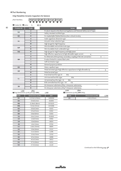
【电容的型号命名规则】murata电容命名规则电容的型号命名:1、各国电容器的型号命名很不统一,国产电容器的命名由四部分组成:第一部分:用字母表示名称,电容器为C。
第二部分:用字母表示材料。
第三部分:用数字表示分类。
第四部分:用数字表示序号。
2、电容的标志方法:(1)直标法:用字母和数字把型号、规格直接标在外壳上。
(2)文字符号法:用数字、文字符号有规律的组合来表示容量。
文字符号表示其电容量的单位:P、N、u、m、F等。
和电阻的表示方法相同。
标称允许偏差也和电阻的表示方法相同。
小于10pF的电容,其允许偏差用字母代替:B——±0.1pF,C——±0.2pF,D——±0.5pF,F——±1pF。
(3)色标法:和电阻的表示方法相同,单位一般为pF。
小型电解电容器的耐压也有用色标法的,位置靠近正极引出线的根部,所表示的意义如下表所示:颜色黑棕红橙黄绿蓝紫灰耐压 4V 6.3V 10V 16V 25V 32V 40V 50V 63V (4)进口电容器的标志方法:进口电容器一般有6项组成。
第一项:用字母表示类别:第二项:用两位数字表示其外形、结构、封装方式、引线开始及与轴的关系。
第三项:温度补偿型电容器的温度特性,有用字母的,也有用颜色的,其意义如下表所示:序号字母颜色温度系数允许偏差字母颜色温度系数允许偏差 1 A 金+100 R 黄 -220 2 B 灰 +30 S 绿 -330 3 C 黑 0 T 蓝 -470 4 G ±30 U 紫 -750 5 H 棕 -30 ±60 V -1000 6 J ±120 W -1500 7 K ±250 X -2200 8 L 红 -80 ±500 Y -3300 9 M ±1000 Z -4700 10 N ±2500 SL +350~-1000 11 P 橙 -150 YN -800~-5800 备注:温度系数的单位10e -6/℃;允许偏差是 % 。
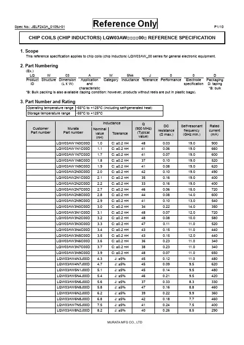
CHIP COILS (CHIP INDUCTORS) LQW03AW□□□□00□ REFERENCE SPECIFICATION1. ScopeThis reference specification applies to chip coils (chip inductors) LQW03AW_00 series for general electronic equipment.2. Part Numbering(Ex.)LQ W 03 A W 5N4 J 0 0 DProductID Structure Dimension(L × W)ApplicationandcharacteristicCategory Inductance Tolerance Performance ElectrodespecificationPackagingD: taping*B: bulk*B: Bulk packing is also available (taping condition: however, products without reels are put in plastic bags).3. Part Number and RatingOperating temperature range -55°C to +125°C (including self-generated heat)Storage temperature range -55°C to +125°CCustomer Part numberMurataPart numberInductance Q(900 MHz)(Typicalvalue)DCresistance(Ω max.)Self-resonantfrequency(GHz min.)Ratedcurrent(mA) Nominalvalue(nH)ToleranceLQW03AW1N0C00D1.0C:±0.2nH 48 0.03 19.0 900 LQW03AW1N1C00D1.1C:±0.2nH 41 0.06 19.0 660 LQW03AW1N7C00D1.7C:±0.2nH 41 0.07 19.0 600 LQW03AW1N8C00D1.8C:±0.2nH 37 0.10 19.0 520 LQW03AW1N9C00D1.9C:±0.2nH 41 0.08 19.0 620 LQW03AW2N0C00D2.0C:±0.2nH 42 0.10 19.0 490 LQW03AW2N1C00D2.1C:±0.2nH 35 0.16 19.0 400 LQW03AW2N2C00D2.2C:±0.2nH 33 0.16 19.0 400 LQW03AW2N7C00D2.7C:±0.2nH 46 0.06 15.0 720 LQW03AW2N8C00D2.8C:±0.2nH 44 0.08 14.0 600 LQW03AW2N9C00D2.9C:±0.2nH 41 0.10 13.0 540 LQW03AW3N0C00D3.0C:±0.2nH 34 0.22 14.0 350 LQW03AW3N1C00D3.1C:±0.2nH 48 0.07 12.0 720 LQW03AW3N2C00D3.2C:±0.2nH 48 0.08 10.0 580 LQW03AW3N3C00D3.3C:±0.2nH 47 0.11 11.0 520 LQW03AW3N4C00D3.4C:±0.2nH 43 0.15 11.0 440 LQW03AW3N5C00D3.5C:±0.2nH 43 0.15 12.0 440 LQW03AW3N6C00D3.6C:±0.2nH 36 0.23 11.0 340 LQW03AW3N7C00D3.7C:±0.2nH 38 0.23 11.0 340 LQW03AW3N9C00D3.9C:±0.2nH 48 0.07 11.0 650 LQW03AW4N3J00D4.3 J:±5% 45 0.12 11.0 480 LQW03AW4N7J00D4.7 J:±5% 45 0.09 9.5 620 LQW03AW5N1J00D5.1 J:±5% 45 0.14 9.5 480 LQW03AW5N4J00D5.4 J:±5% 46 0.21 9.5 420 LQW03AW5N6J00D5.6 J:±5% 37 0.33 8.3 330 LQW03AW5N8J00D5.8 J:±5% 47 0.16 8.8 460 LQW03AW6N2J00D6.2 J:±5% 39 0.22 9.9 360 LQW03AW6N8J00D6.8 J:±5% 42 0.18 7.7 460 LQW03AW7N5J00D7.5 J:±5% 41 0.24 7.5 400 LQW03AW8N2J00D8.2 J:±5% 40 0.26 8.5 290Customer Part numberMurataPart numberInductance Q(900 MHz)(Typicalvalue)DCresistance(Ω max.)Self-resonantfrequency(GHz min.)Ratedcurrent(mA)Nominalvalue(nH)ToleranceLQW03AW8N7J00D8.7J:±5% 39 0.42 7.5 290 LQW03AW9N1J00D9.1J:±5% 46 0.22 6.4 460 LQW03AW10NJ00D10.0J:±5% 37 0.46 7.2 250 LQW03AW11NJ00D11.0J:±5% 37 0.47 7.0 260 LQW03AW12NJ00D12.5J:±5% 39 0.54 6.0 280 LQW03AW13NJ00D13.0J:±5% 39 0.54 5.9 280 LQW03AW14NJ00D13.5J:±5% 37 0.53 6.0 240 LQW03AW15NJ00D15.5J:±5% 38 0.60 5.7 230 4. Testing ConditionsUnless otherwise specified Temperature: ordinary temperature (15°C to 35°C)Humidity: ordinary humidity [25% to 85% (RH)]In case of doubt Temperature: 20°C±2°CHumidity: 60% to 70% (RH)Atmospheric pressure: 86 kPa to 106 kPa5. Appearance and DimensionsUnit mass (typical value): 0.23 mg6. MarkingNo marking.7. Electrical PerformanceNo.ItemSpecificationTest method7.1 InductanceMeet chapter 3 ratings.Measuring equipment: Keysight E4991A or the equivalentMeasuring frequency: Inductance 250 MHz 1.0 nH to 3.9 nH 100 MHz 4.3 nH to 15.5 nH Measuring conditions:Measurement signal level: Approx. 0 dBm Measurement terminal distance: 0.3 mm Electrical length: 10.0 mmMeasuring fixture: Keysight 16197APosition the chip coil under test as shown in the measuring example below and connect it to the electrode by applying weight. Measurement example:Measuring method: see "Electrical performance: Measuring method for inductance/Q" in the chapter"16. Appendix".7.2 QMeet chapter 3 ratings.7.3 DC resistance Meet chapter 3 ratings. Measuring equipment: digital multimeter 7.4 Self-resonantfrequency Meet chapter 3 ratings.Measuring equipment: Keysight N5230A or theequivalent7.5 Rated currentProduct temperature rise: 20°C max.Apply the rated current specified in chapter 3.8. Mechanical PerformanceNo.ItemSpecificationTest method8.1 Bending testNo significant mechanical damage or no sign of electrode peeling off shall be observed. Test substrate: glass-epoxy substrate (100 mm × 40 mm × 0.8 mm) Pressurizing speed: 1 mm/sDeflection: 2 mm Holding time: 5 s8.2 VibrationAppearance shall have no significant mechanical damage.Oscillation frequency: 10 Hz to 55 Hz to 10 Hz, for approx. 1 minTotal amplitude: 1.5 mmTest time: 3 directions perpendicular to each other, 2 h for each direction (6 h in total)No.ItemSpecificationTest method8.3 Solderability90% or more of the outer electrode shall be covered with new solder seamlessly. Flux: immersed in ethanol solution [including anactivator with a chlorine conversion value of 0.06(wt)%]with a rosin content of 25(wt)% for 5 s to 10 s. Solder: Sn-3.0Ag-0.5Cu solderPre-heating: 150°C±10°C/60 s to 90 s Solder temperature: 240°C±5°C Immersion time: 4 s±1 s 8.4 Resistance tosoldering heatAppearance: No significant mechanical damage shall be observed.Inductance change rate: within ±5%Flux: immersed in ethanol solution [including anactivator with a chlorine conversion value of 0.06(wt)%] with a rosin content of 25(wt)% for 5 s to 10 s. Solder: Sn-3.0Ag-0.5Cu solderPre-heating: 150°C±10°C/60 s to 90 s Solder temperature: 270°C±5°C Immersion time: 5 s±1 sPost-treatment: left at a room condition for 24 h±2 h9. Environmental PerformanceThe product is soldered on a substrate for test. No. Item Specification Test method9.1 Heat resistanceAppearance: No significant mechanicaldamage shall be observed.Inductance change rate: within ±5%Q change rate: within ±20%Temperature: 125°C±2°CTest time: 1000 h (+48 h, -0 h)Post-treatment: left at a room condition for 24 h±2 h 9.2 Cold resistanceAppearance: No significant mechanical damage shall be observed.Inductance change rate: within ±5% Q change rate: within ±20%Temperature: -55°C±2°CTest time: 1000 h (+48 h, -0 h)Post-treatment: left at a room condition for 24 h±2 h9.3 HumidityAppearance: No significant mechanical damage shall be observed.Inductance change rate: within ±5% Q change rate: within ±20%Temperature: 70°C±2°CHumidity: 90% (RH) to 95% (RH) Test time: 1000 h (+48 h, -0 h)Post-treatment: left at a room condition for 24 h±2 h 9.4 Temperature cycle Appearance: No significant mechanicaldamage shall be observed.Inductance change rate: within ±5% Q change rate: within ±20%Single cycle conditions:Step 1: -55°C±2°C/30 min±3 minStep 2: ordinary temperature/10 min to 15 min Step 3: +125°C±2°C/30 min±3 minStep 4: ordinary temperature/10 min to 15 min Number of testing: 10 cyclesPost-treatment: left at a room condition for 24 h±2 h10. Specification of Packaging10.1 Appearance and dimensions of tape (8 mm width/paper tape)A (0.52)B (0.65) t 0.75 max.(in mm)10.2 Taping specificationsPacking quantity (Standard quantity) 10000 pcs/reelPacking method The products are placed in embossed cavities of a base tape and sealed by a cover tape.Feed hole position The feed holes on the base tape are on the right side when the cover tape is pulled toward the user. JointThe base tape and the cover tape are seamless.Number of missing productsNumber of missing products within 0.025% of the number per reel or 1 pc., whichever is greater, and are not continuous. The specified quantity per reel is kept.10.3 Break down force of tapeBreak down force of cover tape5 N min.10.4 Peeling off force of cover tapeSpeed of peeling off 300 mm/minPeeling off force0.1 N to 0.6 N (The lower limit is for typical value.)10.5 Dimensions of leader section, trailer section and reelA vacant section is provided in the leader (start) section and trailer (end) section of the tape for the product. The leader section is further provided with an area consisting only of the cover tape (or top tape). (See the diagram below.)10.6 Marking for reelCustomer part number, Murata part number, inspection number (*1), RoHS marking (*2), quantity, etc. *1 Expression of inspection No.: □□ ○○○○(1) (2) (3)(1) Factory code(2) Date First digit: year/last digit of yearSecond digit: month/Jan. to Sep.→1 to 9, Oct. to Dec.→O, N, D Third, Fourth digit: day (3) Serial No.*2 Expression of RoHS marking: ROHS- Y ( ) (1) (2)(1) RoHS regulation conformity(2) Murata classification number10.7 Marking on outer box (corrugated box)Customer name, purchasing order number, customer part number, Murata part number, RoHS marking (*2), quantity, etc.FCover tapetape165°to 180゜10.8 Specification of outer boxDimensions of outer box(mm) Standard reel quantity in outer box (reel)WDH186 186 935* Above outer box size is typical. It depends on a quantity of an order.11. Caution11.1 Restricted applicationsPlease contact us before using our products for the applications listed below which require especially high reliability for the prevention of defects which might directly cause damage to the third party's life, body or property. (1) Aircraft equipment (2) Aerospace equipment (3) Undersea equipment (4) Power plant controlequipment(5) Medical equipment (6) Transportation equipment (vehicles, trains, ships, etc.) (7) Traffic signal equipment (8) Disaster/crimeprevention equipment(9) Data-processing equipment (10) Applications of similar complexity and/or reliability requirements to the applications listed in the above11.2 Precautions on ratingAvoid using in exceeded the rated temperature range, rated voltage, or rated current.Usage when the ratings are exceeded could lead to wire breakage, burning, or other serious fault.11.3 Inrush currentIf an inrush current (or pulse current or rush current) that significantly exceeds the rated current is applied to the product, overheating could occur, resulting in wire breakage, burning, or other serious fault.11.4 Corrosive gasPlease refrain from use since contact with environments with corrosive gases (sulfur gas [hydrogen sulfide, sulfur dioxide, etc.], chlorine, ammonia, etc.) or oils (cutting oil, silicone oil, etc.) that have come into contact with the previously stated corrosive gas environment will result in deterioration of product quality or an open from deterioration due to corrosion of product electrode, etc. We will not bear any responsibility for use under these environments.12. Precautions for UseThis product is for use only with reflow soldering. It is designed to be mounted by soldering. If you want to use other mounting method, for example, using a conductive adhesive, please consult us beforehand.Also, if repeatedly subjected to temperature cycles or other thermal stress, due to the difference in the coefficient of thermal expansion with the mounting substrate, the solder (solder fillet part) in the mounting part may crack.The occurrence of cracks due to thermal stress is affected by the size of the land where mounted, the solder volume, and the heat dissipation of the mounting substrate. Carefully design it when a large change in ambient temperature is assumed.12.1 Land dimensionsThe following diagram shows the recommended land dimensions for reflow soldering.The land dimensions are designed in consideration of electrical characteristics and mountability. Use of other landdimensions may preclude achievement of performance. In some cases, it may result in poor solderability, including positional shift. If you use other land pattern, consider it adequately.a 0.23b 0.65c 0.4(in mm)WDLabelH12.2 Flux and solder usedFlux• Use a rosin-based flux that includes an activator with a chlorine conversion value of 0.06(wt)% to 0.1(wt)%. • Do not use a highly acidic flux with a halide content exceeding 0.2(wt)% (chlorine conversion value). • Do not use a water-soluble flux.Solder• Use Sn-3.0Ag-0.5Cu solder.• Standard thickness of solder paste: 80 μm to 100 μmIf you want to use a flux other than the above, please consult our technical department.12.3 Soldering conditions (reflow)• Pre-heating should be in such a way that the temperature difference between solder and product surface is limited to 150°C max.Cooling into solvent after soldering also should be in such a way that the temperature difference is limited to 100°C max. Insufficient pre-heating may cause cracks on the product, resulting in the deterioration of product quality. • Standard soldering profile and the limit soldering profile is as follows.The excessive limit soldering conditions may cause leaching of the electrode and/or resulting in the deterioration of product quality.Standard profile Limit profilePre-heating 150°C to 180°C/90 s±30 s 150°C to 180°C/90 s±30 s HeatingAbove 220°C/30 s to 60 sAbove 230°C/60 s max.Peak temperature 245°C±3°C 260°C/10 s Number of reflow cycles2 times2 times12.4 Reworking with soldering ironDo not perform reworking with a soldering iron on this product.12.5 Solder volumeSolder shall be used not to increase the volume too much.An increased solder volume increases mechanical stress on the product. Exceeding solder volume may cause the failure of mechanical or electrical performance.Limit ProfileStandard Profile90s±30s230℃260℃245℃±3℃220℃30s~60s60s max.180150Temp.(s)(℃)Time.12.6 Product's locationThe following shall be considered when designing and laying out PCBs.(1) PCB shall be designed so that products are not subject to mechanical stress due to warping the board. [Products direction]Products shall be located in the sideways direction (length: a < b) to the mechanical stress.(2) Components location on PCB separationIt is effective to implement the following measures, to reduce stress in separating the board.It is best to implement all of the following three measures; however, implement as many measures as possible to reduce stress.Contents of measures Stress level(1) Turn the mounting direction of the component parallel to theboard separation surface.A > D *1 (2) Add slits in the board separation part.A >B (3) Keep the mounting position of the component away from the board separation surface.A > C*1 A > D is valid when stress is added vertically to the perforation as with hand separation. If a cutting disc is used, stress will be diagonal to the PCB, therefore A > D is invalid.(3) Mounting components near screw holesWhen a component is mounted near a screw hole, it may be affected by the board deflection that occurs during the tightening of the screw.Mount the component in a position as far away from the screw holes as possible.12.7 Handling of substrateAfter mounting products on a substrate, do not apply any stress to the product caused by bending or twisting to the substrate when cropping the substrate, inserting and removing a connector from the substrate or tightening screw to the substrate. Excessive mechanical stress may cause cracking in the product.Bending Twisting〈Poor example 〉〈Good example〉ba12.8 CleaningThe product shall be cleaned under the following conditions.(1) The cleaning temperature shall be 60°C max. If isopropyl alcohol (IPA) is used, the cleaning temperature shall be 40°Cmax.(2) Perform ultrasonic cleaning under the following conditions. Exercise caution to prevent resonance phenomenon inmounted products and the PCB.Item RequirementPower 20 W/L max.Time 5 min max.Frequency 28 kHz to 40 kHz(3) CleanerAlcohol-based cleaner: IPAAqueous agent: PINE ALPHA ST-100S(4) There shall be no residual flux or residual cleaner. When using aqueous agent, rinse the product with deionized wateradequately and completely dry it so that no cleaner is left.* For other cleaning, consult our technical department.12.9 Storage and transportationStorage period Use the product within 12 months after delivery.If you do not use the product for more than 12 months, check solderability before using it.Storage conditions • The products shall be stored in a room not subject to rapid changes in temperature and humidity.The recommended temperature range is -10°C to +40°C. The recommended relative humidityrange is 15% to 85%.Keeping the product in corrosive gases, such as sulfur, chlorine gas or acid, oxidizes theelectrode, resulting in poor solderability or corrosion of the coil wire of the product.• Do not keep products in bulk packaging. Doing so may cause collision between the products orbetween the products and other products, resulting in core chipping or wire breakage.• Do not place the products directly on the floor; they should be placed on a palette so that they arenot affected by humidity or dust.• Avoid keeping the products in a place exposed to direct sunlight, heat or vibration.Transportation Excessive vibration and impact reduces the reliability of the products. Exercise caution whenhandling the products.12.10 Resin coatingThe inductance value may change due to high cure-stress of resin to be used for coating/molding products.A wire breakage issue may occur by mechanical stress caused by the resin, amount/cured shape of resin, or operatingcondition etc. Some resin contains some impurities or chloride possible to generate chlorine by hydrolysis under some operating condition may cause corrosion of wire of coil, leading to wire breakage.So, please pay your careful attention when you select resin in case of coating/molding the products with the resin.Prior to use the coating resin, please make sure no reliability issue is observed by evaluating products mounted on your board.12.11 Handling of product• Sharp material such as a pair of tweezers or other material such as bristles of cleaning brush, shall not be touched to the winding portion to prevent the breaking of wire.• Mechanical shock should not be applied to the products mounted on the board to prevent the breaking of the core.12.12 Handling with mounting equipment• With some types of mounting equipment, a support pin pushes up the product from the bottom of the base (paper) tape when the product is sucked with the pick-up nozzle.When using this type of equipment, detach the support pin to prevent the breaking of wire on the product.• In some cases, the laser recognition function of the mounting equipment may not recognize this product correctly.Please contact us when using laser recognition. (There is no problem with the permeation and reflection type.)13. Note(1) Please make sure that your product has been evaluated in view of your specifications with our product being mounted toyour product.(2) You are requested not to use our product deviating from the reference specifications.(3) The contents of this reference specification are subject to change without advance notice. Please approve our productspecifications or transact the approval sheet for product specifications before ordering.14. AppendixElectrical performance: Measuring method for inductance/Q (Q measurement is applicable only when the Q value is included in the rating table.)Perform measurement using the method described below. (Perform correction for the error deriving from the measuring terminal.)(1) Residual elements and stray elements of the measuring terminal can be expressed by the F parameter for the 2-poleterminal as shown in the figure below.(2) The product's impedance value (Zx) and measured impedance value (Zm) can be expressed as shown below, by usingthe respective current and voltage for input/output.Zm=V1I1Zx=V2I2(3) Thus, the relationship between the product's impedance value (Zx) and measured impedance value (Zm) is as follows.Zx=αZm-β1-ZmΓHere,α=D/A=1β=B/D=Zsm - (1 - Yom Zsm) ZssΓ=C/A=YomZsm: measured impedance of short chipZss: residual impedance of short chip (0.480 nH)Yom: measured admittance when measuring terminal is open (4) Calculate inductance Lx and Qx using the equations shown below.Lx=Im (Zx)2πfLx: inductance of chip coilQx: Q of chip coilf: measuring frequencyQx=Im (Zx) Re (Zx)。
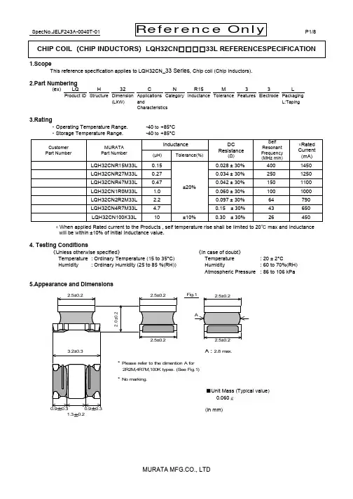
CHIP COIL(CHIP INDUCTORS)LQH32CN□□□□33L REFERENCESPECIFICATION 1.ScopeThis reference specification applies to LQH32CN_33 Series, Chip coil (Chip Inductors).2.Part Numbering(ex)LQ H 32 C N R15 M 3 3 LProduct ID Structure Dimension Applications Category Inductance Tolerance Features Electrode Packaging(L×W)and L:TapingCharacteristics3.Rating・Operating Temperature Range.-40 to+85°C・Storage Temperature Range.-40 to+85°CCustomer Part NumberMURATAPart NumberInductance DCResistance(Ω)SelfResonantFrequency(MHz min)∗RatedCurrent(mA)(µH) Tolerance(%)LQH32CNR15M33L0.15±20% 0.028 ± 30% 400 1450LQH32CNR27M33L 0.27 0.034 ± 30% 250 1250LQH32CNR47M33L 0.47 0.042 ± 30% 150 1100LQH32CN1R0M33L 1.0 0.060 ± 30% 100 1000LQH32CN2R2M33L 2.2 0.097 ± 30% 64 790LQH32CN4R7M33L 4.7 0.15 ± 30% 43 650LQH32CN100K33L 10 ±10% 0.30 ± 30% 26 450 ∗ When applied Rated current to the Products , self temperature rise shall be limited to 20 max and Inductance℃will be within ±10% of initial Inductance value.4. Testing Conditions《Unless otherwise specified》 《In case of doubt》Temperature : Ordinary Temperature (15 to 35°C)Temperature : 20 ± 2°CHumidity : Ordinary Humidity (25 to 85 %(RH))Humidity : 60 to 70%(RH)Atmospheric Pressure : 86 to 106 kPa5.Appearance and Dimensions■Unit Mass (Typical value)0.060g(in mm)A forFig.1)A:2.8m ax.1.3±0.26.Electrical PerformanceNo. Item Specification TestMethod6.1 Inductance Inductance shall meet item 3. Measuring Equipment:KEYSIGHT 4192A or equivalentMeasuring Frequency:1MHz6.2 DC Resistance DC Resistance shall meet item 3. Measuring Equipment:Digital multi meter6.3 Self ResonantFrequency(S.R.F)S.R.F shall meet item 3. Measuring Equipment:KEYSIGHT E4991A or equivalent8.Environmental Performance (It shall be soldered on the substrate.)No. Item Specification TestMethod8.1 Heat Resistance Appearance:No damageInductance Change: within ± 5%DC Resistance Change:within ± 5% Temperature: 85±2°CTime: 1000h (+48h , -0h)Then measured after exposure in the room condition for 24±2 hours.8.2 Cold Resistance Temperature: -40±2°CTime: 1000h (+48h , -0h)Then measured after exposure in the room condition for24±2 hours.8.3 Humidity Temperature: 40±2°CHumidity: 90~95%(RH)Time: 1000h (+48h , -0h)Then measured after exposure in the room condition for24±2 hours.8.4 TemperatureCycle 1 cycle:1 step: -40±2°C / 30±3 minutes2 step: Ordinary temp. / 10 to 15 minutes3 step: +85±2°C / 30±3 min4 step: Ordinary temp. / 10 to 15 minutesTotal of 10 cyclesThen measured after exposure in the room condition for 24±2 hours.9. Specification of Packaging9.1 Appearance and Dimensions of plastic tape(in mm)9.2 Specification of Taping(1) Packing quantity (standard quantity)2,000 pcs / reel(2) Packing MethodProducts shall be packed in the each embossed cavity of plastic tape and sealed by cover tape.(3) Sprocket holeThe sprocket holes are to the right as the tape is pulled toward the user.(4) Spliced pointPlastic tape and Cover tape has no spliced point.(5) Missing components numberMissing components number within 0.1 % of the number per reel or 1 pc., whichever is greater, and arenot continuous. The specified quantity per reel is kept.9.3 Pull StrengthEmbossed carrier tape 10N min.Cover tape 5N min.9.4 Peeling off force of cover tapeSpeed of Peeling off 300mm/minPeeling off force0.2 to 0.7N(minimum value is typical)165to180degreeF Cover tapePlastic tape2.1±0.1※The packing directions of the chip coil in taping are unified with the in/out positions of the lead wire.Dimension of the Cavity is measuredat the bottom side.9.5 Dimensions of Leader-tape, Trailer and ReelThere shall be leader-tape (cover tape) and trailer-tape (empty tape) as follows.9.6 Marking for reelCustomer part number, MURATA part number, Inspection number(∗1), RoHS marking(∗2), Quantity etc ・・・∗1) <Expression of Inspection No.> □□ OOOO ×××(1) (2) (3)(1) Factory Code (2) Date First digit : Year / Last digit of year Second digit : Month / Jan. to Sep. → 1 to 9, Oct. to Dec. → O, N, D Third, Fourth digit : Day (3) Serial No.∗2) « Expression of RoHS marking » ROHS – Y (△)(1) (2)(1) RoHS regulation conformity(2) MURATA classification number9.7 Marking for Outside package (corrugated paper box)Customer name, Purchasing order number, Customer part number, MURATA part number, RoHS marking (∗2) ,Quantity, etc ・・・9.8. Specification of Outer CaseOuter Case Dimensions (mm)Standard Reel Quantityin Outer Case (Reel)W D H 186 186 935∗ Above Outer Case size is typical. It depends on a quantity of an order.Limitation of ApplicationsPlease contact us before using our products for the applications listed below which require especially high reliability for the prevention of defects which might directly cause damage to the third party's life, body or property.(1) Aircraft equipment (6) Transportation equipment (vehicles, trains, ships, etc.) (2) Aerospace equipment (7) Traffic signal equipment(3) Undersea equipment(8) Disaster prevention / crime prevention equipment (4) Power plant control equipment (9) Data-processing equipment(5) Medical equipment (10) Applications of similar complexity and /or reliability requirementsto the applications listed in the aboveWDLabelH11. NoticeThis product is designed for solder mounting.Please consult us in advance for applying other mounting method such as conductive adhesive.11.1 Land pattern designingRecommended land patterns for flow and reflow soldering are as follows: These have been designed for Electric characteristics and solderability.Please follow the recommended patterns. Otherwise, their performance which includes electrical performance or solderability may be affected, or result to "position shift" in soldering process.Flow Soldering Reflow Soldering ∗ (in mm)∗ Applicable to flow soldering.11.2 Flux, SolderFlux ・Use rosin-based flux.・Don’t use highly acidic flux with halide content exceeding 0.2(wt)% (chlorine conversion value).・Don’t use water-soluble flux. Solder・Use Sn-3.0Ag-0.5Cu solder・Standard thickness of solder paste : 200μm to 300μm11.3 Flow soldering conditions / Reflow soldering conditions・Pre-heating should be in such a way that the temperature difference between solder and product surface is limited to 150°C max. Cooling into solvent after soldering also should be in such a way that the temperature difference is limited to 100°C max.Insufficient pre-heating may cause cracks on the product, resulting in the deterioration of product quality. ・Standard soldering profile and the limit soldering profile is as follows.The excessive limit soldering conditions may cause leaching of the electrode and / or resulting in the deterioration of product quality.Soldering profile(1)Flow soldering profileStandard Profile Limit Profile Pre-heating 150℃、60s min.Heating 250℃、4s ~6s 265±3℃℃、5s Cycle of flow2 times1 timeResist265℃±3℃Heating Time150Limit ProfileStandard Profile(s)Time.Temp.(℃)60s min.250℃(2)Reflow soldering profileStandard Profile Limit Profile Pre-heating 150~180°C 、90s±30s Heating above 220°C 、30s ~60s above 230°C 、60s max.Peak temperature 245±3°C 260°C,10s Cycle of reflow2 times1 time11.4 Reworking with soldering iron.The following conditions must be strictly followed when using a soldering iron.Pre-heating 150°C,1 min Tip temperature 350°C max. Soldering iron output 80W max. Tip diameter φ3mm max. Soldering time3(+1,-0)sTimes 2 timesNote : Do not directly touch the products with the tip of the soldering iron in order to prevent the crack on the products due to the thermal shock.11.5 Solder Volume・Solder shall be used not to be exceed the upper limits as shown below.・Accordingly increasing the solder volume, the mechanical stress to Chip is also increased. Exceeding solder volume may cause the failure of mechanical or electrical performance.1/3T ≦ t ≦T(T: Lower flange thickness)11.6 Product's locationThe following shall be considered when designing and laying out P.C.B.’s.(1) P.C.B. shall be designed so that products are not subject to the mechanical stress due to warping the board.[Products direction ]Products shall be located in the sideways direction (Length:a<b) to the mechanical stress.〈Poor example 〉〈Good example 〉baLimit ProfileStandard Profile 90s±30s230℃260℃245℃±3℃220℃30s~60s60s max.180150Temp.(s)(℃)Time.(2) Components location on P.C.B. separation.It is effective to implement the following measures, to reduce stress in separating the board.It is best to implement all of the following three measures; however, implement as many measures as possible to reduce stress.Contents of Measures Stress Level(1) Turn the mounting direction of the component parallel tothe board separation surface.A> D *1(2) Add slits in the board separation part. A> B(3) Keep the mounting position of the component away fromthe board separation surface.A> C*1 A > D is valid when stress is added vertically tothe perforation as with Hand Separation.If a Cutting Disc is used, stress will be diagonal to(3) Mounting Components Near Screw HolesWhen a component is mounted near a screw hole,it may be affected by the board deflection that occursduring the tightening of the screw. Mount the componentin a position as far away from the screw holes as possible.11.7 Cleaning ConditionsProducts shall be cleaned on the following conditions.(1) Cleaning temperature shall be limited to 60°C max.(40°C max for IPA.)(2) Ultrasonic cleaning shall comply with the following conditions with avoiding the resonance phenomenon atthe mounted products and P.C.B.Power : 20 W / l max. Frequency : 28kHz to 40kHz Time : 5 minutes max.(3) Cleaner1. Alternative cleaner・Isopropyl alcohol (IPA)2. Aqueous agent・PINE ALPHA ST-100S(4) There shall be no residual flux and residual cleaner after cleaning.In the case of using aqueous agent, products shall be dried completely after rinse with de-ionized water inorder to remove the cleaner.(5) Other cleaningPlease contact us.11.8 Resin coatingThe inductance value may change due to high cure-stress of resin to be used for coating/molding products. An open circuit issue may occur by mechanical stress caused by the resin, amount/cured shape of resin, or operating condition etc. Some resin contains some impurities or chloride possible to generate chlorine by hydrolysis under some operating condition may cause corrosion of wire of coil, leading to open circuit. So, please pay your careful attention when you select resin in case of coating/molding the products with the resin.Prior to use the coating resin, please make sure no reliability issue is observed by evaluating products mounted on your board.11.9 Caution for use・Sharp material such as a pair of tweezers or other material such as bristles of cleaning brush, shall not be touched to the winding portion to prevent the breaking of wire.・Mechanical shock should not be applied to the products mounted on the board to prevent the breaking of the core11.10 Handling of a substrateAfter mounting products on a substrate, do not apply any stress to the product caused by bending or twisting to the substrate when cropping the substrate, inserting and removing a connector from the substrate or tightening screw to the substrate.Excessive mechanical stress may cause cracking in the product.Bending TwistingSeamSlitADBCbaLength:a<b11.11 Storage and Handling Requirements(1) Storage periodUse the products within 12 months after delivered.Solderability should be checked if this period is exceeded.(2) Storage conditions・Products should be stored in the warehouse on the following conditions.Temperature : -10 ~ 40°CHumidity : 15 to 85% relative humidity No rapid change on temperature and humidityThe electrode of the products is coated with solder. Don't keep products in corrosive gases such as sulfur,chlorine gas or acid, or it may cause oxidization of electrode, resulting in poor solderability.・Products should not be stored on bulk packaging condition to prevent the chipping of the core and the breakingof winding wire caused by the collision between the products.・Products should be stored on the palette for the prevention of the influence from humidity, dust and so on.・Products should be stored in the warehouse without heat shock, vibration, direct sunlight and so on.(3) Handling ConditionCare should be taken when transporting or handling product to avoid excessive vibration or mechanical shock.12. Note(1) Please make sure that your product has been evaluated in view of your specifications with our product being mountedto your product.(2) You are requested not to use our product deviating from the reference specifications.(3) The contents of this reference specification are subject to change without advance notice. Please approve ourproduct specifications or transact the approval sheet for product specifications before ordering。

村田钽电容型号
村田(Murata)钽电容型号命名规则较为复杂,但其通常包含以下几个方面的信息:
1. 尺寸:表示电容的尺寸,如1206、1808等,通常采用国际通用尺寸表示法(单位
为毫米)。
2. 容量:电容的容量,通常用单位为微法的数字表示,如680000μF。
3. 工作电压:电容的工作电压,用字母和数字表示,如V(6.3V)、X(10V)等。
4. 温度特性:表示电容温度特性的字母,如Z(-55℃至125℃)、R(-55℃至85℃)等。
5. 精度:电容的精度,用字母表示,如A(±1%)、B(±2%)等。
6. 材质:表示电容内部材料的字母,如C(陶瓷)、M(金属)等。
7. 特殊属性:表示电容特殊属性的字母,如S(开关)、L(低漏)等。
以村田一款钽电容为例,其型号可能为:1206Z5U106M。
这款电容的解读如下:
- 1206:表示电容尺寸为1206(单位为毫米),属于小型电容。
- Z:表示工作温度范围为-55℃至125℃,适用于一般环境。
- 5:表示电容精度为±5%。
- 106:表示电容容量为106微法。
- M:可能表示电容的材质为陶瓷。
需要注意的是,不同品牌和类型的电容命名规则可能有所不同。
在实际应用中,建议参考具体产品的规格书以了解详细参数。
村田电容选型手册一、引言村田电容作为一家全球领先的电子组件制造商,为各个行业提供高品质、高性能的电容产品。
在电子设备设计中,电容选型是非常重要的一个环节,可以直接影响设备的性能和可靠性。
本手册将介绍村田电容的选型方法和注意事项,帮助工程师选择最适合的电容产品。
二、电容的基本知识1.电容的定义:电容是指两个导体之间的储存电荷的能力大小,单位为法拉(F)。
一般情况下,电容是由两个金属板(电极)和介质组成的。
2.电容的参数:在选型过程中,需要了解以下几个重要的电容参数:-额定电容值(容量):电容器储存电荷的能力,单位为法拉(F)或其它较小的单位如微法(F)。
-额定电压:电容器允许承受的最高电压。
-工作温度范围:电容器能够在哪个温度下正常工作。
-等效串联电阻(ESR):电容器的电阻,会导致电容器产生能量损耗。
-介质:电容器中两个金属板之间的绝缘材料。
3.电容的类型:根据介质的不同,电容器可以分为电解电容、陶瓷电容和塑料电容等。
三、村田电容的产品系列村田电容提供多种电容产品系列,适用于各个行业的不同需求。
以下是村田电容的主要产品系列:1.常规陶瓷电容(GCM)-特点:具有高品质和高性能,适用于低频电路和通信设备。
-应用:手机、电视、DVD播放器等消费电子产品。
2.高性能多层陶瓷电容(HMK)-特点:具有较高的容量和较低的ESR,适用于高频电路和射频应用。
-应用:无线通信设备、雷达设备等。
3.电解电容(ELC)-特点:具有大容量和较高的电压承受能力,适用于电源电路和高精度设备。
-应用:电源适配器、电动车控制器、太阳能逆变器等。
4.高温电容(HCK)-特点:具有较高的工作温度范围和较低的ESR,适用于高温环境。
-应用:汽车电子、电动工具等高温环境下的设备。
四、电容选型方法在进行电容选型时,需要全面考虑电路的要求、性能参数和环境条件。
以下是一些常用的电容选型方法和注意事项:1.确定电容的额定电压:根据电路的工作电压确定电容的额定电压,应选择比工作电压略高一些的容量值。
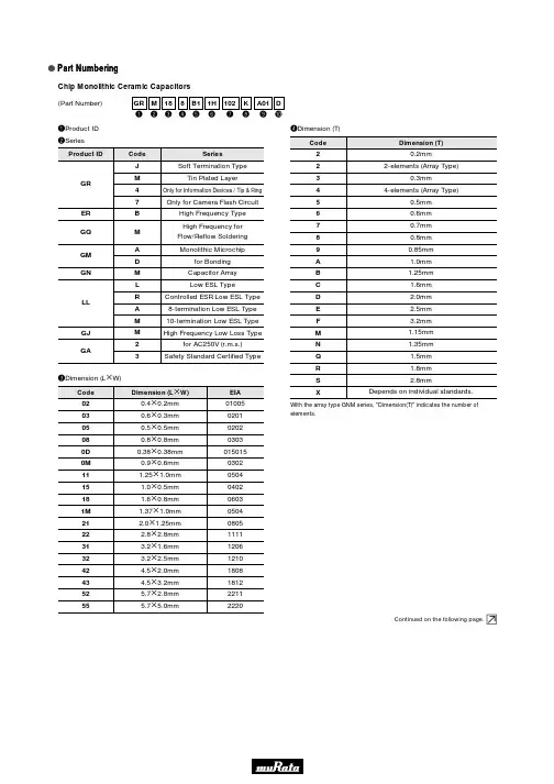
murata电容命名规则【原创版】目录1.Murata 电容的命名规则概述2.Murata 电容的命名规则详解3.实例分析4.总结正文【Murata 电容的命名规则概述】Murata 电容是一家全球领先的电子元器件制造商,其生产的电容器广泛应用于各种电子设备中。
为了方便工程师和技术人员选用和购买,Murata 电容有一套独特的命名规则。
本文将详细解析这一规则,帮助大家更好地理解和应用。
【Murata 电容的命名规则详解】Murata 电容的命名规则主要包括以下几个部分:1.第一个字母:代表电容器的类型。
Murata 电容主要有四种类型,分别是陶瓷电容(C)、钽电容(T)、铝电解电容(A)和薄膜电容(F)。
这四种类型的电容器在性能、尺寸、电压等方面有所不同,第一个字母就是用来区分它们的。
2.前两位数字:代表电容器的尺寸。
这两位数字越大,电容器的体积就越大。
电容器的尺寸通常与其额定电压、容值和稳定性等性能指标有关。
3.第三个字母:代表电容器的精度等级。
Murata 电容的精度等级分为五个级别,分别是 M、K、Z、Y 和 X。
精度等级越高,电容器的容差就越小,性能越稳定。
4.后面的数字:代表电容器的容值。
容值越大,电容器储存的电能就越多。
在选择电容器时,需要根据实际应用场景选择合适的容值。
5.特殊字母和符号:代表电容器的其他性能指标。
例如,Murata 电容的耐压值、温度系数、绝缘等级等性能指标可以通过特殊字母和符号来表示。
【实例分析】以一个 Murata 电容的型号“C0805C104K500”为例,我们可以分析出以下信息:- 类型:陶瓷电容(C)- 尺寸:0805(较小)- 精度等级:C(较高)- 容值:10nF(较小)- 特殊字母和符号:无(表示没有特殊性能要求)【总结】通过了解 Murata 电容的命名规则,我们可以快速准确地了解其电容器的类型、尺寸、精度等级、容值等重要性能指标,为电子设备的设计和选型提供方便。
第一部分电阻日系:世界排名第一:murata(村田),TDK(东电化),AVX-Kyocera(京瓷),Taiyo-Yuden(太阳诱电),Panasonic(松下--已停产);韩系:排名第二--Samsung(三星)台系:Yageo(国巨),Walsin(华新),Dafon(达方),厚声电子封装英制(mil)公制(mm)额定功率@70°C最大工作电压(V)020106031/20W/25040210051/16W/50060316081/16W1/10W50080520121/10W1/8W150120632161/8W1/4W200121032251/4W1/3W200181248321/2W/200201050253/4W200251264321W/200E24精度为5%的碳膜电阻,以欧姆为单位的标称值:1.0 5.633160820 3.9K20K100K510K2.7M1.1 6.236180910 4.3K22K110K560K3M1.2 6.8392001K 4.7K24K120K620K 3.3M1.37.543220 1.1K 5.1K27K130K680K 3.6M1.58.247240 1.2K 5.6K30K150K750K 3.9M1.69.151270 1.3K 6.2K33K160K820K 4.3M1.81056300 1.5K 6.6K36K180K910K 4.7M2.01162330 1.6K7.5K39K200K1M 5.1M2.21268360 1.8K8.2K43K220K 1.1M 5.6M2.413753902K9.1K47K240K 1.2M 6.2M2.71582430 2.2K10K51K270K 1.3M 6.8M3.01691470 2.4K11K56K300K 1.5M7.5M3.318100510 2.7K12K62K330K 1.6M8.2M3.6201105603K13K68K360K 1.8M9.1M3.922120620 3.2K15K75K390K2M10M4.324130680 3.3K16K82K430K 2.2M15M4.727150750 3.6K18K91K470K 2.4M22M5.130E96精度为1%的金属膜电阻,以欧姆为单位的标称值:10331003321K 3.32K10.5K34K107K357K 10.233.2102340 1.02K 3.4K10.7K34.8K110K360K 10.534105348 1.05K 3.48K11K35.7K113K365K 10.734.8107350 1.07K 3.57K11.3K36K115K374K 1135.7110357 1.1K 3.6K11.5K36.5K118K383K 11.336113360 1.13K 3.65K11.8K37.4K120K390K 11.536.5115365 1.15K 3.74K12K38.3K121K392K 11.837.4118374 1.18K 3.83K12.1K39K124K402K 1238.3120383 1.2K 3.9K12.4K39.2K127K412K 12.139121390 1.21K 3.92K12.7K40.2K130K422K 12.439.2124392 1.24K 4.02K13K41.2K133K430K 12.740.2127402 1.27K 4.12K13.3K42.2K137K432K 1341.2130412 1.3K 4.22K13.7K43K140K442K 13.342.2133422 1.33K 4.32K14K43.2K143K453K 13.743137430 1.37K 4.42K14.3K44.2K147K464K 1443.2140432 1.4K 4.53K14.7K45.3K150K470K 14.344.2143442 1.43K 4.64K15K46.4K154K475K 14.745.3147453 1.47K 4.7K15.4K47K158K487K 1546.4150464 1.5K 4.75K15.8K47.5K160K499K 15.447154470 1.54K 4.87K16K48.7K162K511K 15.847.5158475 1.58K 4.99K16.2K49.9K165K523K 1648.7160487 1.6K 5.1K16.5K51K169K536K 16.249.9162499 1.62K 5.11K16.9K51.1K174K549K 16.551165510 1.65K 5.23K17.4K52.3K178K560K16.951.1169511 1.69K 5.36K17.8K53.6K180K562K17.452.3174523 1.74K 5.49K18K54.9K182K576K 17.853.6178536 1.78K 5.6K18.2K56K187K590K 1854.9180549 1.8K 5.62K18.7K56.2K191K604K 18.256182560 1.82K 5.76K19.1K57.6K196K619K18.756.2187562 1.87K 5.9K19.6K59K200K620K19.157.6191565 1.91K 6.04K20K60.4K205K634K 19.659196578 1.96K 6.19K20.5K61.9K210K649K 2060.42005902K 6.2K21K62K215K665K 20.561.9205604 2.05K 6.34K21.5K63.4K220K680K 2162210619 2.1K 6.49K22K64.9K221K681K 21.563.4215620 2.15K 6.65K22.1K66.5K226K698K 2264.9220634 2.2K 6.8K22.6K68K232K715K 22.166.5221649 2.21K 6.81K23.2K68.1K237K732K22.668226665 2.26K 6.98K23.7K69.8K240K750K23.268.1232680 2.32K7.15K24K71.5K243K768K 23.769.8237681 2.377.32K24.3K73.2K249K787K 2471.5240698 2.4K7.5K24.9K75K255K806K 24.373.2243715 2.43K7.68K25.5K76.8K261K820K 24.775249732 2.49K7.87K26.1K78.7K267K825K24.975.5255750 2.55K8.06K26.7K80.6K270K845K25.576.8261768 2.61K8.2K27K82K274K866K26.178.7267787 2.67K8.25K27.4K82.5K280K887K 26.780.6270806 2.7K8.45K28K84.5K287K909K 2782274820 2.74K8.66K28.7K86.6K294K910K 27.482.5280825 2.8K8.8K29.4K88.7K300K931K 2884.5287845 2.87K8.87K30K90.9K301K953K28.786.6294866 2.94K9.09K30.1K91K309K976K29.488.7300887 3.0K9.1K30.9K93.1K316K 1.0M 3090.9301909 3.01K9.31K31.6K95.3K324K 1.5M 30.191309910 3.09K9.53K32.4K97.6K330K 2.2M30.993.1316931 3.16K9.76K33K100K332K31.695.3324953 3.24K10K33.2K102K340K32.497.6330976 3.3K10.2K33.6K105K348K第二部分电容电容分类电容的种类首先要按照介质种类来分。