809芯片
- 格式:docx
- 大小:37.37 KB
- 文档页数:3
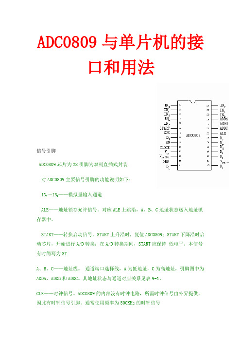
ADC0809与单片机的接口和用法信号引脚ADC0809芯片为28引脚为双列直插式封装.对ADC0809主要信号引脚的功能说明如下:IN7~IN——模拟量输入通道ALE——地址锁存允许信号。
对应ALE上跳沿,A、B、C地址状态送入地址锁存器中。
START——转换启动信号。
START上升沿时,复位ADC0809;START下降沿时启动芯片,开始进行A/D转换;在A/D转换期间,START应保持低电平。
本信号有时简写为ST.A、B、C——地址线。
通道端口选择线,A为低地址,C为高地址,引脚图中为ADDA,ADDB和ADDC。
其地址状态与通道对应关系见表9-1。
CLK——时钟信号。
ADC0809的内部没有时钟电路,所需时钟信号由外界提供,因此有时钟信号引脚。
通常使用频率为500KHz的时钟信号EOC ——转换结束信号。
EOC=0,正在进行转换;EOC=1,转换结束。
使用中该状态信号即可作为查询的状态标志,又可作为中断请求信号使用。
D 7~D 0——数据输出线。
为三态缓冲输出形式,可以和单片机的数据线直接相连。
D 0为最低位,D 7为最高OE ——输出允许信号。
用于控制三态输出锁存器向单片机输出转换得到的数据。
OE=0,输出数据线呈高阻;OE=1,输出转换得到的数据。
Vcc —— +5V 电源。
Vref ——参考电源参考电压用来与输入的模拟信号进行比较,作为逐次逼近的基准。
其典型值为+5V(Vref (+)=+5V, Vref (-)=-5V).接法一:ST EOC 01234567ALE CC BB AA OE76543210EOC ALE ST OE AA BB CCXTAL218XTAL119ALE 30EA31PSEN 29RST9P0.0/AD039P0.1/AD138P0.2/AD237P0.3/AD336P0.4/AD435P0.5/AD534P0.6/AD633P0.7/AD732P1.0/T21P1.1/T2EX 2P1.23P1.34P1.45P1.56P1.67P1.78P3.0/RXD 10P3.1/TXD 11P3.2/INT012P3.3/INT113P3.4/T014P3.7/RD17P3.6/WR 16P3.5/T115P2.7/A1528P2.0/A821P2.1/A922P2.2/A1023P2.3/A1124P2.4/A1225P2.5/A1326P2.6/A1427U1AT89C52VCCGND69%RV110kVCCOUT121ADD B 24ADD A 25ADD C 23VREF(+)12VREF(-)16IN31IN42IN53IN64IN75START 6OUT58EOC 7OE9CLOCK 10OUT220OUT714OUT615OUT817OUT418OUT319IN228IN127IN026ALE 22U2ADC0808U2(IN0)D 2Q5CLK3Q6S4R1U3:A74LS74D 12Q9CLK11Q8S10R13U3:B74LS74主要程序:OE=0;//输出为高阻态AA=BB=CC=0;//选择通道0ALE=1;ST=1;ALE=0;//锁存地址选择通道ST=0;//启动转换While(!EOC);//等待转换结束OE=1;//打开数据通道Value=P0;//读取结果接法二:模拟通道选择信号A、B、C分别接最低三位地址A0、A1、A2即(P0.0、P0.1、P0.2)01234567ALE AA BB CC01234567CCBB AA EOC EOCRD RDWRWRWR XTAL218XTAL119ALE 30EA31PSEN 29RST9P0.0/AD039P0.1/AD138P0.2/AD237P0.3/AD336P0.4/AD435P0.5/AD534P0.6/AD633P0.7/AD732P1.0/T21P1.1/T2EX 2P1.23P1.34P1.45P1.56P1.67P1.78P3.0/RXD 10P3.1/TXD 11P3.2/INT012P3.3/INT113P3.4/T014P3.7/RD17P3.6/WR 16P3.5/T115P2.7/A1528P2.0/A821P2.1/A922P2.2/A1023P2.3/A1124P2.4/A1225P2.5/A1326P2.6/A1427U1AT89C52D02D13D24D35D46D57D68D79Q019Q118Q217Q316Q415Q514Q613Q712LE 11OE 1U374HC573?OUT121ADD B 24ADD A25ADD C 23VREF(+)12VREF(-)16IN31IN42IN53IN64IN75START 6OUT58EOC 7OE9CLOCK 10OUT220OUT714OUT615OUT817OUT418OUT319IN228IN127IN026ALE 22U6ADC080875%RV210k12U4:A74LS0434U4:B74LS04D 2Q5CLK3Q6S 4R1U2:A 74LS74D 12Q9CLK11Q8S10R13U2:B74LS74二分频器主要程序:首先确定ADC0809的地址因为只有P0.0、P0.1、P0.2与adc0809有关,故ADC0809的地址为0xFFF8-0xFFFF 即通道IN0-IN7 #define adc809 PBYTE[0xF8]//选中INT0adc0809=0x07; //adc0809=随便一个数,只产生一个WR=0的脉冲信号,锁存AABBCC 的地址while(!EOC); value=adc809;//读取adc809的值接法三:01234567ALE 01234567EOC EOCRD RDWRWRWR 210XTAL218XTAL119ALE 30EA31PSEN 29RST9P0.0/AD039P0.1/AD138P0.2/AD237P0.3/AD336P0.4/AD435P0.5/AD534P0.6/AD633P0.7/AD732P1.0/T21P1.1/T2EX 2P1.23P1.34P1.45P1.56P1.67P1.78P3.0/RXD 10P3.1/TXD 11P3.2/INT012P3.3/INT113P3.4/T014P3.7/RD17P3.6/WR 16P3.5/T115P2.7/A1528P2.0/A821P2.1/A922P2.2/A1023P2.3/A1124P2.4/A1225P2.5/A1326P2.6/A1427U1AT89C52D02D13D24D35D46D57D68D79Q019Q118Q217Q316Q415Q514Q613Q712LE 11OE 1U374HC573?OUT121ADD B 24ADD A25ADD C 23VREF(+)12VREF(-)16IN31IN42IN53IN64IN75START 6OUT58EOC 7OE9CLOCK 10OUT220OUT714OUT615OUT817OUT418OUT319IN228IN127IN026ALE 22U6ADC080875%RV210k12U4:A74LS0434U4:B74LS04D 2Q5CLK3Q6S 4R1U2:A 74LS74D 12Q9CLK11Q8S10R13U2:B74LS74ADC0809的三个地址端A 、B 、C 即可如前所述与地址线相连,也可与数据线相连,例如ADDA 、ADDB 、ADDC 接到数据口0、1、2,这时启动A/D 转换的指令与上述类似,只不过A 的内容不能为任意数,而必须和所选输入通道号IN 0~IN 7相一致。


内置延时高精度低功耗电压检测■ 产品概述LN809系列是为微处理器和电子系统提供低功耗电压检测芯片,具高精度低温漂的特点。
该系列产品检测电压基本涵盖大部分电子产品的需求。
低静态电流是其重要的优点。
产品系列中包含了CMOS 输出和漏端开路的N 管输出。
由于内置延时,减少了应用电路中的外围器件。
■ 产品特点● 高精度: ± 1%,± 2% ● 低功耗:小于1.5μA● 检测电压点:2.63V,2.93V,3.08V,4.0V,4.38V 和 4.63V ● 工作范围: 0.7V ~6.0V● 检测电压温度特性:±100ppm/℃(TYP.)● 内置延时: 典型值50ms,100ms,200ms,400ms 可选。
●输出方式: N 管漏端开路或CMOS■ 用途● 微处理器复位电路 ● 记忆体电池备份电路 ● 电源上电复位电路 ● 电源无效检测● 系统电池寿命和充电电压监测 ●延迟电路■ 封装● SOT-23-3L ● SOT-23-3B■ 产品订购信息LN809 ①②③④⑤⑥⑦■ 引脚配置 SOT-23-3L/BRESETVSS(TOP VIEW)SOT-23-3Marking 1243■ 打印信息① ② 表示输出类型与检测电压值 CMOS 输出(LN809C 系列)N 管漏开路 (LN809N 系列)③ 表示输出延时 ④ 表示批号 (基于内部标准)■典型应用电路■功能框图■绝对最大额定值■电学特性VDF (T):检测电压点恢复电压:VDR = VDF + VHYS注释: 由于延时电流会具有功耗,在电压恢复后,延时电路作用的时间内,芯片总功耗将大于额定值■典型特性曲线测试产品: VDF=2.63V■操作注释●CMOS 输出(特别地注意第4点)①当Vin端输入电压高于释放电压release voltage (VDR),这个电压将逐步降低。
当VIN端输入电压高于检测电压detectvoltage (VDF),输出电压与输入电压相等。

有关RT809F读写24、25芯片出错问题的解决方法
一:排除系统问题,找台干净的电脑系统,安装好RT809F 软件及驱动,测试运行,若故障没改变,那就是硬件问题。
二:可拆开编程器,插上USB线,连接好电脑,检测一下U3输出电压是否3.3V,若不正确,更换新的。
三:再次打开RT809F软件,测试是否正常使用,若还是不正常,再进一步检测Q14、Q19、Q22、Q23。
(可以使用印字为2TY、正面的Q22和Q23是PNP三极管,
Y2、2A、T06、2AM的PNP三极管代替):
背面的Q14(可以使用印字为J2Y、Y1、1A、T04、1AM 的NPN三极管代替):
Q19是PNP三极管,偶有损坏(可以使用印字为2TY、Y2、2A、T06、2AM的PNP三极管代替)。
编程器常用驱动三极管参数:
印字2TY ,真实型号为S8550,PNP,25V 0.5A
印字Y2,真实型号为SS8550,PNP,25V 1A
印字J3Y ,真实型号为S8050,NPN,25V 0.5A
印字Y1,真实型号为SS8050,NPN,25V 1A
若以上问题排除后,还是没有解决,请联系你购买的商家送修。

MAX809替代料Maxim Semiconductor MAX809芯片可采用TOREX XC61F替换XC61F品牌:TOREX产地:日本特点:内置延迟电路的电压检测器代理商:深圳市泰德兰电子有限公司TOREX XC61F系列为内置延迟电路的电压检测器。
采用CMOS工艺和激光微调技术,实现了高精度,低电流消耗。
检测电压精度高,且温度漂移极小。
输出电路有N沟开漏和CMOS 2种。
因内置延迟电路,所以不需要外置元件,可实现高密度安装。
TOREX XC61F可与Maxim Semiconductor MAX809相媲美,替换MAX809芯片TOREX XC61F检测电压范围能够在1.6V~6.0V范围内以0.1V间隔设定;MAX809检测电压+2.5 V,+3 V,+3.3 V和+5 VTOREX XC61F輸出形式N沟道开漏/CMOS輸出;MAX809輸出形式Push-Pull active-low RESET Output (MAX809)TOREX XC61F内置延迟电路1ms~50ms 50ms~200ms 80ms~400msXC61F特征:高电压检测精度±2%低消耗电流1.0μA(TYP.)[VIN=2.0V]检测电压范围能够在1.6V~6.0V范围内以0.1V间隔设定工作电压范围0.7V~10.0V检测电压温度特性±100ppm/℃(TYP.)内置延迟电路1ms~50ms50ms~200ms80ms~400ms輸出形式N沟道开漏/CMOS輸出小型封装SOT-23, SOT-89, TO-92Highly Accurate : ± 2%Low Power Consumption : 1.0μA(TYP.)[ VIN=2.0V ]Detect V oltage Range : 1.6V ~ 6.0V in 0.1V incrementsOperating V oltage Range : 0.7V ~ 10.0VDetect V oltage Temperature Characteristics:±100ppm/℃(TYP.)Built-In Delay Circuit : ①1ms ~ 50ms②50ms ~ 200ms③80ms ~ 400msOutput Configuration : N-ch open drain output or CMOS Packages : SOT-23: SOT-89: TO-92Environmentally Friendly : EU RoHS Compliant, Pb Free XC61F电路图:XC61F引脚配置:TOREX品牌优势:TOREX以提高客户满足度为目标,Torex取得质量管理系统的国际规格ISO9001本公司所提供之产品,由合作工厂生产。

电压延时功能的复位芯片概述
电压延时功能的复位芯片可以通过检测电源电压的变化,并在电源电压达到某个阈值时,触发复位操作。
这种芯片通常用于微控制器、微处理器或其他数字逻辑电路中,以确保它们在电源电压不稳定或突然掉电时能够安全地复位。
电压延时功能的复位芯片有多种型号,以下是一些常见的品牌和型号:
1. Maxim MAX809/MAX810:这是一种常用的微控制器复位芯片,具有低功耗、高可靠性和低成本的优点。
它可以在电源电压下降到某个阈值时,自动触发复位操作。
2. STMicroelectronics ST1232:这是一种通用型的复位芯片,适用于多种微控制器和数字逻辑电路。
它具有低功耗、高速和低噪声的优点。
3. NXP K5031:这是一种适用于微控制器的复位芯片,具有低功耗、低成本和紧凑的封装尺寸。
它可以在电源电压上升或下降到某个阈值时,触发复位操作。
这些复位芯片都具有可调的电压阈值和延时时间,可以根据具体应用的需求进行配置。
同时,它们都具有低功耗和低噪声的优点,可以有效地延长微控制器的使用寿命和提高系统的稳定性。


POWER MANAGEMENT- Improved Maxim MAX809/MAX810 replacement —Lower supply current…6µA —80% lower maximum supply current - Monitor 5V, 3.3V and 3V supplies - 140ms min. reset pulse width- Active-low reset valid with 1.1V supply (IMP809)- Small 3-pin SOT-23 package - No external components- Specified over full temperature range — -40°C to 105°C- Embedded controllers - Battery operated systems - Intelligent instruments- Wireless communication systems - PDAs and handheld equipmentThe IMP809/IMP810 are 3.0V, 3.3V and 5.0V power supply supervisor circuits optimized for low-power microprocessor (µP), microcontroller (µC) and digital systems. The IMP809/810 are improved drop-in re-placements for the Maxim MAX809/810 and feature 60% lower supply current.A reset signal is issued if the power supply voltage drops below a preset reset threshold and is asserted for at least 140ms after the supply has risen above the reset threshold. The IMP809 has an active-low RE-SET output that is guaranteed to be in the correct state for V CC down to 1.1V. The IMP810 has an active-high RESET output. The reset comparator is designed to ignore fast transients on V CC .Low supply current makes the IMP809/IMP810 ideal for use in portable and battery operated equipment. The IMP809/IMP810 are available in a compact 3-pin SOT23 package. Six voltage thresholds are available to support 3V to 5V systems:Key FeaturesApplicationsGeneral DescriptionR eset ThresholdSuf f i x V olt ag e (V) L 4.63 M 4.38 J 4.00 T 3.08 S 2.93 R 2.63 Z 2.32¯¯¯¯¯¯Pin Assignments(RESET )RESET SOT23GNDV CCIMP809 (IMP810)POWER MANAGEMENTAbsolute Maximum RatingsPin DescriptionsPin N u mberN a me Function1 GNDGround 2 (IMP809)RESET RESET is asserted LOW if V CC falls below the reset threshold and remains LOW for the 240ms typical reset timeout period (140ms minimum) after V CC exceeds the threshold. 2 (IMP810)RESETRESET is asserted HIGH if V CC falls below the reset threshold and remains HIGH for the240ms typical reset timeout period (140ms minimum) after V CC exceeds the threshold.3V CC Power supply input voltage (3.0V , 3.3V , 5.0V) ¯¯¯¯¯¯ ¯¯¯¯¯¯ Pin Terminal Voltage with Respect to GroundV CC . . . . . . . . . . . . . . . . . . . . . . . . . . . . . . . . . –0.3V to 6.0VRESET, RESET . . . . . . . . . . . . . . . . . . . . . . . . . –0.3V to (V CC + 0.3V) Input Current at V CC . . . . . . . . . . . . . . . . . . . 20mA Output Current: RESET, RESET . . . . . . . . . 20mA Rate of Rise at V CC . . . . . . . . . . . . . . . . . . . . 100V/µs Power Dissipation (T A = 70°C) . . . . . . . . . . 320mW (Derate 4mW/°C above 70°C)Operating Temperature Range . . . . . . . . . . –40°C to 105°C Storage Temperature Range . . . . . . . . . . . . . –65°C to 160°C Lead Temperature (soldering, 10 sec) . . . . . 300°CThese are stress ratings only and functional operation is not implied. Exposure to absolute maximum ratings for prolonged time periods may affect device reliability.Block DiagramV CCV CCIMP809 (IMP810)V CCGNDRESET ¯¯¯¯¯¯ InputGNDRESET ¯¯¯¯¯¯ RESETPOWER MANAGEMENTElectrical CharacteristicUnless otherwise noted V CC is over the full voltage range, T A = –40°C to 105°C.Typical values at T A = 25°C, V CC = 5V for L/M/J devices, V CC = 3.3V for T/S devices and V CC = 3V for R devices.V CC=2.5V for Z devicesPOWER MANAGEMENTTypical Performance CharacteristicsReset TimingThe reset signal is asserted–LOW for the IMP809 and HIGH for the IMP810–when the VCC signal falls below the threshold trip voltage and remains asserted for 140ms minimum after the VCC has risen above the threshold.V THActive Reset Timeout Period 140ms minimumIMP809IMP8105V 0V5V 0V 5V 0VRESET RESET¯¯¯¯¯¯ V CCFigure 1. Reset Timing DiagramNegative V CC TransientsThe IMP809/810 protect µPs from brownouts and low V CC . Short duration transients of 100mV amplitude and 20µs or less duration typically do not cause a false RESET. Valid Reset with V CC under 1.1V¯¯¯¯¯¯ ¯¯¯¯¯¯To ensure logic inputs connected to the IMP809 RESET pin are in a known state when VCC is under 1.1V, a 100k Ω pull -down resistor at RESET is needed. The value is not critical. A pull-up resistor to VCC is needed with the IMP810.POWER MANAGEMENTTypical Performance Characteristics(Continued)V CCPowerSupplyGNDIMP810100k ΩRESET V CC Power SupplyGNDIMP809100k ΩRESET ¯¯¯¯¯ Figure 2. RESET Valid with VCC Under 1.1V ¯¯¯¯¯¯¯ Figure 3. RESET Valid with V CC Under 1.1VBi-directional Reset Pin InterfacingThe IMP809/810 can interface with µP/µC bi-directional reset pins by connecting a 4.7k Ω resistor in series with the IMP809/810 reset output and the µP/µC bi-directional reset pin.Power SupplyV CCIMP809RESET ¯¯¯¯¯¯ GNDBUF4.7k ΩBuffered RESET ¯¯¯¯¯¯µC or µPRESET ¯¯¯¯¯¯ InputGNDBi-directional I/O Pin(Example: 68HC11)Figure 4. Bi-directional Reset Pin InterfacingPOWER MANAGEMENTOrdering InformationP a c k a g e Mar king2 P a r t N umber1R eset Threshold(V)T e mper ature R ang e Pin-Pac k a g e(XXX L o t Code) IMP809 Active LOW ResetIMP809LEUR-T 4.63 –40°C to+105°C3-SOT23AAXXX IMP809MEUR-T 4.38–40°C to+105°C3-SOT23ABXXX IMP809JEUR-T 4.00–40°C to+105°C3-SOT23CWXXX IMP809TEUR-T 3.08–40°C to+105°C3-SOT23ACXXX IMP809SEUR-T 2.93–40°C to+105°C3-SOT23ADXXX IMP809REUR-T 2.63–40°C to+105°C3-SOT23AFXXX IMP809ZEUR-T 2.32–40°C to+105°C3-SOT23ZAXXX IMP810 Active HIGH ResetIMP810LEUR-T 4.63 –40°C to+105°C3-SOT23AGXXX IMP810MEUR-T 4.38–40°C to+105°C3-SOT23AHXXX IMP810JEUR-T 4.00–40°C to+105°C3-SOT23AIXXX IMP810TEUR-T 3.08–40°C to+105°C3-SOT23AJXXX IMP810SEUR-T 2.93–40°C to+105°C3-SOT23AKXXX IMP810REUR-T 2.63–40°C to+105°C3-SOT23ALXXX IMP810ZEUR-T 2.32–40°C to+105°C3-SOT23ZBXXXNotes: 1. Tape and Reel packaging is indicated by the -T designation.2. Devices may also be marked with full part number: 809L, 810M etc. XXX refers to lot.Related ProductsIMP809IMP810IMP811IMP812 Max.Supply Current15µA15µA15µA15µA Package Pins3344Manual RESET input■■Package T ype SOT-23SOT-23SOT-143SOT-143 Active-HIGH RESET output■■Active-LOW RESET output■■POWER MANAGEMENTMechanical DimensionsPlastic SOT-23 (3-Pin)POWER MANAGEMENTISO 9001 RegisteredDaily Silver IMP Microelectronics Co.,Ltd7 keda Road ,Hi-Tech Park,NingBo,Zhejiang,P.R.CPost Code:315040Tel:(086)-574-87906358Fax:(086)-574-87908866Email:sales@ The IMP logo is a registered trademark of Daily Silver IMP. All other company and product names are trademarks of their respective owners @2009 Daily Silver IMP Printed in china Revision: FIssue Date: 14th.Jun.09 Type: Product。

S P 809 / S P 8103 P i n M i c r o p r o c e s s o r S u p e r v i s o r C i r c u i tGENERAL DESCRIPTIONThe SP809/SP810 are low power microprocessor (μP) supervisory circuits used to monitor power supp lies in μP and digital systems.They provide applications with benefits of circuit reliability and low cost by eliminating external components. If the VCC supply voltage falls below preset threshold then a reset signal is asserted for at least 140ms after V CC has risen above the reset threshold. Both the SP809 and SP810 were designed with a reset comparator to help identify invalid signals, which last less than 140ms. The onlydifference between them is that they have an active-low RESET output and active-high RESET output, respectively. Low supply current (1μA) makes SP809/SP810 ideal for portable equipment.The devices are available in 3 pin SOT-23 package.Part NumberOutput Type SP809N Open Drain Active LowSP809 Push-Pull Low SP810Push-Pull Active HighAPPLICATIONS• Portable Electronic Devices • Electrical Power Meters • Digital Still Cameras • µP Power MonitoringFEATURES• Ultra Low Supply Current 1µA (typ) • Guaranteed Reset valid to V CC = 0.9V • 140ms Power-On Reset Pulse Width • Internally Fixed Threshold2.3V, 2.6V, 2.9V,3.1V,4.4V, 4.6V • 1.5% Voltage Threshold Tolerance • 3 Pin SOT-23 PackageTYPICAL APPLICATION DIAGRAMFig. 1: SP809 / SP810 Application DiagramABSOLUTE MAXIMUM RATINGSThese are stress ratings only and functional operation of the device at these ratings or any other above those indicated in the operation sections of the specifications below is not implied. Exposure to absolute maximum rating conditions for extended periods of time may affect reliability.V CC .......................................................... -0.3V to 6.5V RESET, RESET...................................... -0.3V to V CC+0.3V Output Current (RESET, RESET) ............................... 20mA Power Dissipation (T A=70°C) .............................. 320mW Junction Temperature .......................................... 125°C Storage Temperature .............................. -65°C to 150°C OPERATING RATINGSInput Voltage Range V CC ................................ 0.9V to 6V Junction Temperature Range ..................... -40°C to 85°CELECTRICAL SPECIFICATIONSSpecifications with standard type are for an Operating Temperature of T A= 25°C only; limits applying over the full Operating Temperature range are denoted by a “•”. Minimum and Maximum limits are guaranteed through test, design, or statistical correlation. Typical values represent the most likely parametric norm at T A = 25°C, and are provided for reference purposes only. Unless otherwise indicated, T A= 25°C.Note 1: RESET output is for SP809; RESET output is for SP810.BLOCK DIAGRAMFig. 2: SP809 / SP810 Block Diagram PIN ASSIGNMENTFig. 3: SP809 / SP810 Pin Assignment PIN DESCRIPTIONORDERING INFORMATION (1)Part NumberOperating Temperature Range Lead-Free Package Packing MethodSP809EK-L-2-3/TR -40°C≤T A ≤+85°C Yes (2) SOT23-3 Tape & ReelSP809EK-L-2-6/TR SP809EK-L-2-9/TR SP809EK-L-3-1/TR (3) SP809EK-L-4-6/TR (3) SP809NEK-L-2-3/TR (3)SP809NEK-L-2-9/TR (3) SP809NEK-L-3-1/TR SP809NEK-L-4-6/TR (3) SP810EK-L-4-4/TR (3) NOTES:1. Refer to /SP809 and /SP810 for most up-to-date Ordering Information.2. Visit for additional information on Environmental Rating.3. NRND – Not Recommended for New Designs.TYPICAL PERFORMANCE CHARACTERISTICSAll data taken at T A = 25°C, unless otherwise specified - Schematic and BOM from Application Information section of thisdatasheet.Fig. 4: Supply Current versus TemperatureFig. 5: Power-Down Reset Delay versus TemperatureFig. 6: Power-Down Reset Delay versus TemperatureFig. 7: Power-Down Reset Delay versus TemperatureFig. 8: Normalized Reset Threshold versus TemperatureFig. 9: Power-Up Reset Time-out versus TemperatureTHEORY OF OPERATIONμP will be activated at a valid reset state. These μP supervisory circuits assert reset to prevent code execution errors during power-up,power-down, or brownout conditions. Reset is guaranteed to be a logic low for V TH>V CC>0.9V. Once V CC exceeded the reset threshold, an internal timer keeps RESET low for the reset timeout period; after this interval, RESET goes high.If a brownout condition occurs (V CC drops below the reset threshold), RESET goes low. Any time V CC goes below the reset threshold, the internal timer resets to zero, and RESET goes low. The internal timer is activated after V CC returns above the reset threshold, and RESET remains low for the reset timeout period.B ENEFIT OF H IGHLY A CCURATE R ESETT HRESHOLDSP809/810 with specified voltage as 5V±10% or 3V±10% are ideal for systems using a 5V±5% or 3V±5% power supply. The reset is guaranteed to assert after the power supply falls below the minimum specified operating voltage range of the system ICs. The pre-trimmed thresholds are reducing the range over which an undesirable reset may occur.Fig. 10: Timing WaveformsAPPLICATION INFORMATIONN EGATIVE G OING V CC T RANSIENTSIn addition to issuing a reset to the µP during power-up, power-down, and brownout conditions, SP809 series are relatively resistant to short-duration negative-going V CC transient.E NSURING A V ALID R ESET O UTPUT D OWNTO V CC=0When V CC falls below 0.9V, SP809 RESET output no longer sinks current; it becomes an open circuit. In this case, high-impedance CMOS logic inputs connecting to RESET can drift to undetermined voltages. Therefore, SP809/810 with CMOS is perfect for most applications of V CC down to 0.9V.However in applications where RESET must be valid down to 0V, adding a pull-down resistor to RESET causes any leakage currents to flow to ground, holding RESET low. I NTERFACING TO µP WITH B IDIRECTIONALR ESET P INSThe RESET output on the SP809N is open drain, this device interfaces easily with μPs that have bidirectional reset pins. Connecting the μP supervisor's RESET output directly to the microcontroller's RESET pin with a single pull-up resistor allows either device to assert reset. T EST C IRCUITFig. 11: Test CircuitPACKAGE SPECIFICATION 3-P IN SOT23REVISION HISTORYRevision Date Description2.0.0 2011 Reformat of DatasheetCorrection of package drawing2.0.1 August 2017 Correct Reset Delay conditions. Updated to MaxLinear logo. Updated format and ordering information table.2.0.2November 2017Corrected typo from rev 2.0.1, added 2 missing overlines to RESET in ElectricalSpecifications.Corporate Headquarters: 5966 La Place Court Suite 100Carlsbad, CA 92008 Tel.:+1 (760) 692-0711 Fax: +1 (760) 444-8598 High Performance Analog: 1060 Rincon Circle San Jose, CA 95131 Tel.: +1 (669) 265-6100 Fax: +1 (669) 265-6101Email: ************************* The content of this document is furnished for informational use only, is subject to change without notice, and should not be construed as a commitment by MaxLinear, Inc.. MaxLinear, Inc. assumes no responsibility or liability for any errors or inaccuracies that may appear in the informational content contained in this guide. Complying with all applicable copyright laws is the responsibility of the user. Without limiting the rights under copyright, no part of this document may be reproduced into, stored in, or introduced into a retrieval system, or transmitted in any form or by any means (electronic, mechanical, photocopying, recording, or otherwise), or for any purpose, without the express written permission of MaxLinear, Inc.Maxlinear, Inc. does not recommend the use of any of its products in life support applications where the failure or malfunction of the product can reasonably be expected to cause failure of the life support system or to significantly affect its safety or effectiveness. Products are not authorized for use in such applications unless MaxLinear, Inc. receives, in writing, assurances to its satisfaction that: (a) the risk of injury or damage has been minimized; (b) the user assumes all such risks; (c) potential liability of MaxLinear, Inc. is adequately protected under the circumstances.MaxLinear, Inc. may have patents, patent applications, trademarks, copyrights, or other intellectual property rights covering subject matter in this document. Except as expressly provided in any written license agreement from MaxLinear, Inc., the furnishing of this document does not give you any license to these patents, trademarks, copyrights, or other intellectual property. Company and product names may be registered trademarks or trademarks of the respective owners with which they are associated.。

sgm809复位原理SGM809是一款CMOS电源监测IC,具有复位功能。
复位功能是指当系统出现异常或不稳定时,通过将IC引脚置低,使系统返回到初始状态,从而保证系统的稳定性和可靠性。
本文将详细介绍SGM809的复位原理。
SGM809的复位原理是基于自适应阈值的电压检测电路实现的。
它具有精确的复位阈值,可适用于各种电压应用环境。
SGM809有一个内部的参考电压源,其阈值和温度特性已经被校准。
通过与外部电压参考源相连接,以提供更高的准确性和稳定性。
SGM809的复位阈值可以通过外部电阻器与VCC引脚相连接来设定。
复位阈值的设定范围是从1.0V到4.6V。
当系统电压低于复位阈值时,SGM809的复位引脚(RESET)会被拉低。
SGM809的电压复位特性是在电压监测器(Voltage Detector)和电压参考源之间的比较中实现的。
当电压监测器检测到系统电压低于复位阈值时,它会关闭输出驱动器,将RESET引脚拉低,使系统进入复位状态。
SGM809的复位引脚带有一个双脉冲重启电路,该电路可以确保在短暂的电源中断或扰动的情况下,系统能快速恢复正常工作。
双脉冲重启电路通过将RESET引脚拉低然后拉高来实现。
拉低RESET引脚会将系统复位,而拉高RESET引脚则会解除复位状态,使系统进入正常工作状态。
SGM809还具有一个超低功耗特性,它能够有效地降低系统功耗,在电池供电的情况下,能够延长电池寿命。
当系统进入低功耗模式时,SGM809可以通过根据外部引脚状态选择不同的工作模式来降低功耗。
这些工作模式包括普通模式和低功耗模式。
总结起来,SGM809是一款具有复位功能的电源监测IC。
它通过自适应阈值的电压检测电路来实现复位功能。
当系统电压低于复位阈值时,SGM809的复位引脚会被拉低,使系统进入复位状态。
同时,SGM809还具有双脉冲重启电路和超低功耗特性,以确保系统能够快速恢复正常工作并降低功耗。


Philips SemiconductorsProduct dataMAX809/MAX8103-pin microprocessor resetsSOT23-3: plastic small outline package; 3 leads; body width 1.5 mm1.351.21.00.250.500.250.220.083.002.701.701.500.550.352310.150.0510°0°Philips SemiconductorsProduct dataMAX809/MAX8103-pin microprocessor resetsSC70-3:plastic small outline package; 3 leads; body width 1.15 mm1.00.80.40.250.2250.102.11.90.40.1Philips Semiconductors Product data 3-pin microprocessor resetsMAX809/MAX810 REVISION HISTORY Rev _3 Date 20030808 Description Product data (9397 750 11889; ECN 853–2355 30184 dated 04 August 2003. SupersedesMAX809_MAX810_2 of 2002 Oct 21 (9397 750 10584. • Add ‘Marking code’ table to Ordering information on page 3. • SOT23–3 package outline on page 9 corrected. _2 _1 20021021 20020620 Product data (9397 750 10584; ECN 853–2355 29047 dated 14 October 2002. Supersedes MAX809_MAX810_1 of 2002 June 20 (9397 750 10213. Product data (9397 750 10213; ECN 853–2355 28505 dated 20 June 2002. Modifications: 2003 Aug 08 11Philips Semiconductors Product data 3-pin microprocessor resetsMAX809/MAX810 Data sheet status Level I Data sheet status [1] Objective data Product status [2] [3] Development Definitions This data sheet contains data from the objective specification for product development. Philips Semiconductors reserves the right to change the specification in any manner without notice. This data sheet contains data from the preliminary specification. Supplementary data will be published at a later date. Philips Semiconductors reserves the right to change the specification without notice, in order to improve the design and supply the best possible product. This data sheet contains data from the product specification. Philips Semiconductors reserves the right to make changes at any time in order to improve the design, manufacturing and supply. Relevant changes will be communicated via a Customer Product/Process Change Notification (CPCN. II Preliminary data Qualification III Product data Production [1] Please consultthe most recently issued data sheet before initiating or completing a design. [2] The product status of the device(s described in this data sheet may have changed since this data sheet was published. The latest information is available on the Internet at URL . [3] For data sheets describing multiple type numbers, the highest-level product status determines the data sheet status. Definitions Short-form specification — The data in a short-form specification is extracted from a full data sheet with the same type number and title. For detailed information see the relevant data sheet or data handbook. Limiting values definition — Limiting values given are in accordance with the Absolute Maximum Rating System (IEC 60134. Stress above one or more of the limiting values may cause permanent damage to the device. These are stress ratings only and operation of the device at these or at any other conditions above those given in the Characteristics sections of the specification is not implied. Exposure to limiting values for extended periods may affect device reliability. Application information — Applications that are described herein for any of these products are for illustrative purposes only. Philips Semiconductors make no representation or warranty that such applications will be suitable for the specified use without further testing or modification. Disclaimers Life support — These products are not designed for use in life support appliances, devices, or systems where malfunction of these products can reasonably be expected to result in personal injury. Philips Semiconductors customers using or selling these products for use in such applications do so at their own risk and agree to fully indemnify Philips Semiconductors for any damages resulting from such application. Right to make changes — Philips Semiconductors reserves the right to make changes in the products—including circuits, standard cells, and/or software—described or contained herein in order to improve design and/or performance. When the product is in full production (status ‘Production’, relevant changes will be communicated via a Customer Product/Process Change Notification (CPCN. Philips Semiconductors assumes no responsibility or liability for the use of any of these products, conveys no license or title under any patent, copyright, or mask work right to these products, and makes norepresentations or warranties that these products are free from patent, copyright, or mask work right infringement, unless otherwise specified. Contact information For additional information please visit . Fax: +31 40 27 24825 © Koninklijke Philips Electronics N.V. 2003 All rights reserved. Printed in U.S.A. Date of release: 08-03 For sales offices addresses send e-mail to:sales.addresses@. Document order number: 9397 750 11889 Philips Semiconductors 2003 Aug 08 12This datasheet has been downloaded from: Free Download Daily Updated Database 100% Free Datasheet Search Site 100% Free IC Replacement Search Site Convenient Electronic Dictionary Fast Search System All Datasheets Cannot Be Modified Without Permission Copyright © Each Manufacturing Company。

mx809芯片工作原理
MX809是一款无线通信芯片,其工作原理主要通过以下几个步骤:
1. 射频信号接收:MX809芯片中集成了射频前端模块,可以接收到无线信号。
当信号进入芯片后,首先经过射频放大器进行放大,然后经过射频滤波器进行滤波,以去除不必要的频率干扰。
2. 数字信号处理:经过射频前端模块处理后,信号进入数字信号处理部分。
MX809芯片中包含了模数转换器(ADC)和数字信号处理器(DSP)。
ADC将模拟信号转换为数字信号,然后DSP对数字信号进行处理和解码。
3. 数据解码与检错:MX809芯片中的DSP可以对接收到的数字信号进行解码,并对接收到的数据进行校验。
通过检查数据的校验码,可以判断数据是否传输正确,并对错误进行纠正或重传。
4. 数据处理与存储:MX809芯片中的DSP还可以对接收到的数据进行处理和存储。
例如,在进行无线通信时,可以对接收到的语音或图像进行压缩和解压缩,以减少数据传输的带宽和延迟。
5. 射频信号发送:MX809芯片不仅可以接收射频信号,还可以发送射频信号。
经过数字信号处理后,DSP将数字信号转换为射频信号,并通过射频放大器进行放大,最后通过天线发
送出去。
总体来说,MX809芯片通过射频模块接收、处理和发送无线信号,通过数字信号处理和数据处理实现无线通信。
它的工作原理是将射频信号转换为数字信号进行处理和传输。

封装MAX809MAX809概述是一款应用于数字系统供电电源电压监控的电压检测芯片,可在工业级标准温度范围内工作。
产生一个复位信号,当系统电源电压降低到设定值时复位信号变低,当系统电源电压恢复到设定值之后芯片会在至少140ms 的延迟时间之后将复位信号置高。
系列产品可以提供任意客户需要的设定检测电压值。
目前我们会提供7个针对5.0V ,3.3V ,3.0V 和2.5V 四类电源电压的标准工业用电压监测值。
提供推挽结构的输出级,当待监测电压高于设定电压值时复位输出高电平。
快速的电源瞬态的抖动和毛刺会被本芯片滤除而不会导致误动作,同时即便供电电压低至1.0V 也能够保证正常的输出逻辑和各性能指标。
提供紧凑的3脚封装形式SOT-23特性◆可工作于工业级温度范围内: -40℃ to +85℃ ◆可低至1V 正常工作 ◆电源毛刺干扰屏蔽功能 ◆提供SOT-23 ◆符合无铅和 RoHS 要求应用范围◆电脑,服务器,笔记本,调制解调器 ◆无线交换机 ◆嵌入式系统 ◆家电,电表◆PDA 和手持设备采用SOT-23典型应用PowerMAX809MAX809MAX809MAX809打标说明及管脚分布SOT-23GNDRESET管脚描述MAX809R MAX809S MAX809T 型号 最高输入电压(V)复位电压(V)容差封装形式SOT23 SOT89-35.5 3.08+2% 5.5 2.93 +2%5.52.63+2%丝印AFAAADAA ACAA ■ 型号选择结构框图VDD注: 超过上表所列的“绝对最大额定值”的应用条件有可能会永久性损害芯片。
此处仅指额定极限指标,并不暗示客户可以将本芯片应用在此条件下或者其他任何超过“推荐工作条件”下。
所有超过“绝对最大额定值”的应用都会影响本芯片的可靠性。
电气特性(如无特别说明,环境温度TA=25℃)MAX MAX809使用说明复位信号将给微处理器一个确定的初始状态,将会给出这样一个复位信号,以防止微处理器在电源上电、下电或者掉电的过程中出现代码执行的错误。


rk809应用场景一、什么是rk809rk809是一款集成了充电管理芯片和电源管理芯片的电池管理芯片,可以广泛应用于各种移动设备和嵌入式系统中。
它具有高度集成、低功耗、高精度和可靠性强等特点,因此在很多应用场景中得到了广泛的应用。
二、rk809的特点rk809具有以下几个特点:1. 高度集成rk809集成了充电管理芯片和电源管理芯片,可以同时实现对电池的充电和电源的管理,大大简化了系统设计和布局。
2. 低功耗rk809采用了先进的功耗管理技术,可以有效降低系统的功耗,延长电池的续航时间,提高系统的稳定性。
3. 高精度rk809内置了高精度的电流电压检测电路,可以实时监测电池的电流和电压,保证充电的安全性和稳定性。
4. 可靠性强rk809采用了多重保护机制,包括过压保护、过流保护、过温保护等,可以有效保护电池和系统的安全。
三、rk809的应用场景rk809可以广泛应用于各种移动设备和嵌入式系统中,以下是几个常见的应用场景:1. 手机和平板电脑在手机和平板电脑中,rk809可以实现对电池的充电管理和电源的管理,确保电池的安全充电和系统的稳定运行。
同时,rk809还可以监测电池的电流和电压,提供给系统进行电量显示和电池健康状态的判断。
2. 可穿戴设备在可穿戴设备中,由于体积和功耗的限制,对电池管理的要求更高。
rk809的高度集成和低功耗特点使其成为可穿戴设备的理想选择。
它可以实现对电池的充电管理和电源的管理,同时还可以提供精确的电流和电压监测,满足可穿戴设备对电池管理的需求。
3. 智能家居设备在智能家居设备中,rk809可以用于电池供电的设备,如智能门锁、智能摄像头等。
它可以实现对电池的充电管理和电源的管理,保证设备的稳定运行。
同时,rk809还可以监测电池的电流和电压,提供给系统进行电量显示和电池健康状态的判断。
4. 工业控制设备在工业控制设备中,对电池管理的要求更为严格。
rk809的高度集成和可靠性强的特点使其成为工业控制设备的理想选择。

rt809h编程器说明书RT809H编程器是一种专业的芯片编程工具,广泛应用于电子产品的维修和编程工作中。
本篇文章将对RT809H编程器进行详细介绍,包括其功能特点、操作步骤和注意事项等方面内容。
一、功能特点1.支持多种芯片型号:RT809H编程器支持各类常见芯片的编程,如EEPROM、SPI Flash、BIOS、LCD控制器等。
对于不同型号芯片,RT809H可以根据需要进行编程和读取操作,以满足不同维修需求。
2.高速编程:RT809H具有高速编程功能,能够在短时间内完成大批量芯片的编程,提高工作效率。
3.多种编程方式:RT809H编程器支持多种编程方式,如ISP、NAND、I2C等,以适应不同芯片的编程需求。
4.图形化界面:RT809H编程器的操作界面简洁明了,采用图形化设计,用户可以通过操作界面轻松完成编程和设置。
5.联机功能:RT809H编程器具有与电脑联机的功能,用户可以通过USB接口将编程器和电脑进行连接,实现数据传输和固件升级等操作。
二、操作步骤1.准备工作:将RT809H编程器和电脑通过USB接口连接,确保连接稳定。
同时,将待编程的芯片正确插入编程器的芯片座,注意插入方向。
2.打开编程软件:双击打开RT809H编程器的软件,即可进入主界面。
3.选择芯片型号:在软件的菜单栏中选择"芯片型号",然后从列表中选择待编程的芯片型号。
如果列表中没有所需的芯片型号,还可以手动输入芯片参数。
4.设置编程模式:根据芯片的编程方式,选择相应的编程模式。
例如,如果芯片支持ISP编程,则选择ISP模式。
5.读取芯片数据:点击界面上的"读取"按钮,开始读取芯片中的数据。
读取完成后,可以将数据保存至电脑中的指定文件夹。
6.编程操作:在完成读取操作后,可以进行芯片的编程操作。
将需要写入的数据加载到编程器中,然后点击界面上的"编程"按钮,开始进行编程操作。

RT809H编程器教程MS838更换主芯片后重写引导和主程序方法RT809H编程器是一款多功能通用EPROM编程器,能够用于各种芯片的编程和重写。
在使用RT809H编程器时,有时可能需要更换主芯片,并且需要重新编写引导程序和主程序。
本教程将介绍如何使用RT809H编程器来实现这个过程。
步骤1:准备工作首先,准备好你要更换的主芯片,并确保它是全新的。
同时,准备好你要重写的引导程序和主程序的文件。
将这些文件保存在计算机的硬盘上,并确保它们的路径是正确的。
步骤2:连接RT809H编程器将RT809H编程器连接到计算机上。
使用USB数据线将编程器的USB端口连接到计算机的USB接口上。
确保连接正常并且编程器已经成功识别。
步骤3:更换主芯片将需要更换的主芯片插入编程器的芯片插槽中。
确保插入的方向是正确的,并且芯片的引脚没有弯曲或者损坏。
步骤4:打开RT809H编程器软件在计算机上打开RT809H编程器软件。
软件的图标通常位于桌面上或者开始菜单中。
双击图标打开软件。
步骤5:选择芯片型号在软件的主界面上,选择你所使用的芯片型号。
点击软件界面左上角的下拉菜单,选择你要编程的芯片型号。
确保所选的芯片型号与实际芯片型号相匹配。
步骤6:打开引导和主程序文件点击软件界面右下角的“文件”按钮,选择“打开文件”。
在弹出的对话框中,找到你保存引导和主程序文件的路径,并选择它们打开。
步骤7:编写引导和主程序在软件界面的主界面上,找到“引导程序”和“主程序”的选项卡。
点击相应的选项卡,进入相应的界面。
在引导程序界面上,找到“芯片引导程序”选项,并点击它。
在弹出的对话框中,选择你保存的引导程序文件,并点击“确定”按钮。
软件将加载引导程序文件,你可以在界面上看到引导程序的相关信息。
在主程序界面上,找到“芯片主程序”选项,并点击它。
在弹出的对话框中,选择你保存的主程序文件,并点击“确定”按钮。
软件将加载主程序文件,你可以在界面上看到主程序的相关信息。
809芯片
809芯片是一款高性能、低功耗的嵌入式控制芯片,广泛应用
于物联网、智能家居、智能穿戴设备等领域。
本文将从809芯片的核心特性、应用场景以及未来发展方向等方面进行详细介绍。
一、809芯片的核心特性
1. 高性能:809芯片采用先进的处理器架构和高速时钟频率,
能够快速、高效地处理各种复杂的运算任务,满足不同应用场景的需求。
2. 低功耗:809芯片采用先进的功耗管理技术,能够在保证高
性能的同时,有效降低功耗,延长设备的续航时间,提升用户体验。
3. 多核架构:809芯片拥有多核心的处理器结构,能够同时处
理多个任务,提高系统的并行处理能力,保证系统的稳定和高效性能。
4. 多种接口:809芯片支持多种常见的外设接口,包括UART、SPI、I2C等,方便与其他设备进行通信和数据交换。
5. 多种通信模块支持:809芯片支持多种无线通信模块,如蓝牙、Wi-Fi、NFC等,能够实现设备之间的高速数据传输和互
联互通。
二、809芯片的应用场景
1. 物联网:809芯片作为物联网设备的核心控制芯片,可以连
接传感器、执行器等设备,实现物联网设备之间的数据传输和协同工作,广泛应用于智能家居、智能城市、智能农业等领域。
2. 智能家居:809芯片可以作为智能家居设备的控制中心,实
现家电、照明、安防等设备之间的联动控制,提升家居生活的便利性和舒适性。
3. 智能穿戴设备:809芯片的低功耗和高性能使其成为制造智
能手表、智能眼镜等智能穿戴设备的理想选择,能够提供多种功能,如健康监测、运动追踪、消息提醒等。
4. 工业自动化:809芯片可用于工业自动化设备的控制和监控,如机器人、自动化生产线等,能够提升生产效率和产品质量,降低人工成本。
5. 智慧医疗:809芯片可以应用于医疗设备的控制和监测,如
智能健康监测设备、远程医疗等,可以实现患者的远程监护和快速响应,提高医疗质量和效率。
三、809芯片的未来发展方向
1. 更强大的处理能力:随着技术的不断进步,809芯片的处理
能力将会进一步提升,可以处理更加复杂的任务和数据,满足未来物联网和人工智能的需求。
2. 更低的功耗:809芯片在保持高性能的同时,还会进一步降
低功耗,以满足更长续航时间的需求,推动智能设备的发展。
3. 更多的接口和通信模块支持:随着物联网设备和智能设备的不断普及,809芯片将支持更多的接口和通信模块,与其他设
备之间实现更加便捷和高速的数据传输和互联互通。
4. 更高的安全性:在物联网时代,数据安全至关重要,809芯
片将会加强对设备和数据的保护,提供更高的安全性和可靠性,防止数据泄露和攻击。
5. 更广泛的应用场景:809芯片作为一款灵活、高性能的嵌入
式控制芯片,将在更多领域得到应用,如智能交通、智能家居、智慧农业等,为人们的生活和工作带来更多的便利和创新。
总之,809芯片作为一款高性能、低功耗的嵌入式控制芯片,具有多核架构、多种接口和通信模块支持等特性,广泛应用于物联网、智能家居、智能穿戴设备等领域。
随着技术的不断进步,809芯片的性能将不断提升,应用场景将更加广泛,为人们的生活和工作带来更多的便利和创新。