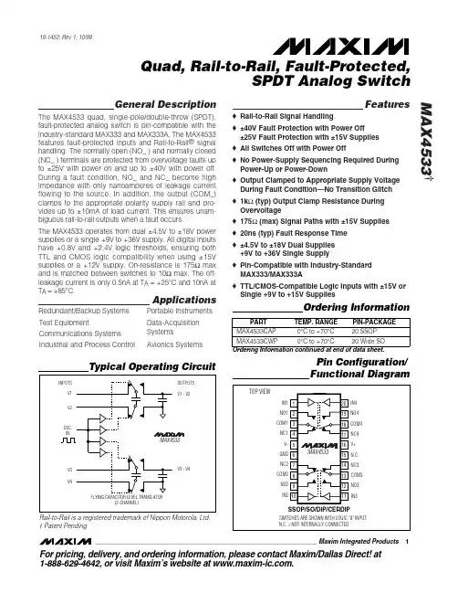
General DescriptionThe MAX4533 quad, single-pole/double-throw (SPDT),fault-protected analog switch is pin-compatible with the industry-standard MAX333 and MAX333A. The MAX4533features fault-protected inputs and Rail-to-Rail ®signal handling. The normally open (NO_ ) and normally closed (NC_ ) terminals are protected from overvoltage faults up to ±25V with power on and up to ±40V with power off.During a fault condition, NO_ and NC_ become high impedance with only nanoamperes of leakage current flowing to the source. In addition, the output (COM_)clamps to the appropriate polarity supply rail and pro-vides up to ±10mA of load current. This ensures unam-biguous rail-to-rail outputs when a fault occurs.The MAX4533 operates from dual ±4.5V to ±18V power supplies or a single +9V to +36V supply. All digital inputs have +0.8V and +2.4V logic thresholds, ensuring both TTL and CMOS logic compatibility when using ±15V supplies or a +12V supply. On-resistance is 175Ωmax and is matched between switches to 10Ωmax. The off-leakage current is only 0.5nA at T A =+25°C and 10nA at T A =+85°C.ApplicationsRedundant/Backup Systems Portable Instruments Test EquipmentData-Acquisition Communications Systems SystemsIndustrial and Process ControlAvionics SystemsFeatureso Rail-to-Rail Signal Handlingo ±40V Fault Protection with Power Off±25V Fault Protection with ±15V Supplies o All Switches Off with Power Offo No Power-Supply Sequencing Required During Power-Up or Power-Down o Output Clamped to Appropriate Supply Voltage During Fault Condition—No Transition Glitch o 1k Ω(typ) Output Clamp Resistance During Overvoltage o 175Ω(max) Signal Paths with ±15V Supplies o 20ns (typ) Fault Response Time o ±4.5V to ±18V Dual Supplies +9V to +36V Single Supplyo Pin-Compatible with Industry-Standard MAX333/MAX333Ao TTL/CMOS-Compatible Logic Inputs with ±15V or Single +9V to +15V SuppliesMAX4533†Quad, Rail-to-Rail, Fault-Protected,SPDT Analog Switch________________________________________________________________Maxim Integrated Products 1Typical Operating Circuit19-1452; Rev 1; 10/99Pin Configuration/Functional DiagramOrdering InformationRail-to-Rail is a registered trademark of Nippon Motorola, Ltd.†Patent PendingFor pricing, delivery, and ordering information,please contact Maxim/Dallas Direct!at 1-888-629-4642, or visit Maxim’s website at .M A X 4533Quad, Rail-to-Rail, Fault-Protected,SPDT Analog SwitchABSOLUTE MAXIMUM RATINGSELECTRICAL CHARACTERISTICS —Dual Supplies(V+ = +15V, V- = -15V, T A = T MIN to T MAX , unless otherwise noted. Typical values are at T A = +25°C.) (Note 3)Stresses beyond those listed under “Absolute Maximum Ratings” may cause permanent damage to the device. These are stress ratings only, and functional operation of the device at these or any other conditions beyond those indicated in the operational sections of the specifications is not implied. Exposure to absolute maximum rating conditions for extended periods may affect device reliability.Voltages Referenced to GNDV+........................................................................-0.3V to +44.0V V-.........................................................................-44.0V to +0.3V V+ to V-................................................................-0.3V to +44.0V COM_, IN_ (Note 1).............................(V- - 0.3V) to (V+ + 0.3V)NC_, NO_ (Note 2)..................................(V+ - 40V) to (V- + 40V)NC_, NO_ to COM_.................................................-40V to +40V NC_, NO_ Overvoltage with Switch Power On(supplies at ±15V)................................................-30V to +30V NC_, NO_ Overvoltage with Switch Power Off........-40V to +40V Continuous Current into Any Terminal..............................±30mA Peak Current into Any Terminal(pulsed at 1ms,10% duty cycle)....................................±50mAContinuous Power Dissipation (T A = +70°C)20-Pin SSOP (derate 10.53mW/°C above +70°C)........842mW 20-Pin Wide SO (derate 10.00mW/°C above +70°C)..800mW 20-Pin Plastic DIP (derate 11.11mW/°C above +70°C)889mW 20-Pin CERDIP (derate 11.11mW/°C above +70°C).....889mW Operating Temperature RangesMAX4533C_ _......................................................0°C to +70°C MAX4533E_ _...................................................-40°C to +85°C MAX4533M_ _.................................................-55°C to +125°C Storage Temperature Range.............................-65°C to +150°C Lead Temperature (soldering, 10s).................................+300°CNote 1:COM_ and IN_ pins are not fault protected. Signals on COM_ or IN_ exceeding V+ or V- are clamped by internal diodes.Limit forward diode current to maximum current rating.Note 2:NC_ and NO_ pins are fault protected. Signals on NC_ or NO_ exceeding -25V to +25V may damage the device. Theselimits apply with power applied to V+ or V-. The limit is ±40V with V+ = V- = 0.MAX4533Quad, Rail-to-Rail, Fault-Protected,SPDT Analog Switch_______________________________________________________________________________________3ELECTRICAL CHARACTERISTICS —Dual Supplies (continued)(V+ = +15V, V- = -15V, T= T to T , unless otherwise noted. Typical values are at T = +25°C.) (Note 3)M A X 4533Quad, Rail-to-Rail, Fault-Protected,SPDT Analog Switch 4_______________________________________________________________________________________ELECTRICAL CHARACTERISTICS —Single Supply(V+ = +12V, V- = 0, T A = T MIN to T MAX , unless otherwise noted. Typical values are at T A = +25°C.) (Note 3)MAX4533Quad, Rail-to-Rail, Fault-Protected,SPDT Analog Switch_______________________________________________________________________________________5Note 3:The algebraic convention is used in this data sheet; the most negative value is shown in the minimum column.Note 4:∆R ON = R ON(MAX)- R ON(MIN).Note 5:Leakage parameters are 100% tested at maximum-rated hot temperature and guaranteed by correlation at T A = +25°C.Note 6:Guaranteed by design.Note 7:Off-isolation = 20log10(V COM_/ V NO_), V COM_= output, V NO_= input to off switch.Note 8:Between any two analog inputs.Note 9:Leakage testing for single-supply operation is guaranteed by testing with dual supplies.ELECTRICAL CHARACTERISTICS —Single Supply (continued)(V+ = +12V, V- = 0, T A = T MIN to T MAX , unless otherwise noted. Typical values are at T A = +25°C.) (Note 3)M A X 4533Quad, Rail-to-Rail, Fault-Protected,SPDT Analog Switch 6_______________________________________________________________________________________Typical Operating Characteristics(V+ = +15V, V- = -15V, T A = +25°C, unless otherwise noted.)906030120150210180240270300330360390-18-12-9-15-6-30369121518ON-RESISTANCE vs. V COM(DUAL SUPPLIES)V COM (V)R O N (Ω)0100502001502503003504000101552025303540ON-RESISTANCE vs. V COM(SINGLE SUPPLY)V COM (V)R O N (Ω)755025100125150175200225250-15-5-10051015ON-RESISTANCE vs. V COM AND TEMPERATURE (DUAL SUPPLIES)V COM (V)R O N (Ω)010050250200150400350300450042681012ON-RESISTANCE vs. V COM AND TEMPERATURE (SINGLE SUPPLY)V COM (V)R O N (Ω)0200100400300500600±4±10±12±6±8±14±16±18TURN-ON/TURN-OFF TIME vs. SUPPLY VOLTAGE (DUAL SUPPLIES)SUPPLY VOLTAGE (V)t O N , t O F F (n s)0.00010.010.00110.1100101000-55-155-3525456585105125ON/OFF-LEAKAGE CURRENTvs. TEMPERATURETEMPERATURE (°C)L E A K A G E C U R R E NT (A )01.00.52.01.53.02.53.54.54.05.0-15-10-5015510CHARGE INJECTION vs. VCOMV COM (V)Q (p C )50150100200250816122024283236TURN-ON/TURN-OFF TIME vs.SUPPLY VOLTAGE (SINGLE SUPPLY)SUPPLY VOLTAGE (V)t O N , t O F F (n s )40208060120100140180160200-55-15525-35456585105125TURN-ON/TURN-OFF TIME vs.TEMPERATURE (DUAL SUPPLIES)TEMPERATURE (°C)t O N , t O F F (n s )MAX4533Quad, Rail-to-Rail, Fault-Protected,SPDT Analog Switch_______________________________________________________________________________________750100150200250-552545-155-356585105125TURN-ON/TURN-OFF TIME vs.TEMPERATURE (SINGLE SUPPLY)TEMPERATURE (°C)t O N , t O F F (n s )-500-300-400-100-2001000200400300500-55-15525-35456585105125POWER-SUPPLY CURRENT vs.TEMPERATURE (DUAL SUPPLIES, V IN = 0)TEMPERATURE (°C)S U P P L Y C U R R E N T (µA )-600-200-4002000600400800-55-155-3525456585105125POWER-SUPPLY CURRENT vs.TEMPERATURE (DUAL SUPPLIES, V IN= +5V)TEMPERATURE (°C)S U P P L Y C U R R E N T (µA )10050250200150350300400-55525-35-15456585105125POWER-SUPPLY CURRENT vs.TEMPERATURE (SINGLE SUPPLY)TEMPERATURE (°C)S U P P L Y C U R R E N T (µA )01.00.52.01.52.53.04812162024283236LOGIC-LEVEL THRESHOLD vs. SUPPLY VOLTAGESUPPLY VOLTAGE (V)L O G I C -L E V E L T H RE S H O L D (V )COM_(10V/div)NO_ or NC_(10V/div)OVOVOVERVOLTAGE WITH ±25V INPUTM A X 4533 t o c 115µs/divTypical Operating Characteristics (continued)(V+ = +15V, V- = -15V, T A = +25°C, unless otherwise noted.)COM_(10V/div)NO_ or NC_(10V/div)OVOVFAULT-FREE SIGNAL WITH ±15V INPUTM A X 4533 t o c 125µs/div COM_(10V/div)NO_ or NC_(10V/div)OVOVFAULT RECOVERY TIMEM A X 4533 t o c 132µs/divM A X 4533Quad, Rail-to-Rail, Fault-Protected,SPDT Analog Switch 8_______________________________________________________________________________________0-1000.010.11101001000FREQUENCY RESPONSE (DUAL SUPPLIES)-80-90-70FREQUENCY (MHz)R E S P O N S E (d B )-60-50-40-30-10-20Typical Operating Characteristics (continued)(V+ = +15V, V- = -15V, T A = +25°C, unless otherwise noted.)-1000.010.11101001000FREQUENCY RESPONSE (SINGLE SUPPLY)-80-90-70FREQUENCY (MHz)R E S P O N S E (d B )-60-50-40-30-10-20Pin DescriptionDetailed DescriptionThe MAX4533 is a fault-protected analog switch with special operation and construction. Traditional fault-pro-tected switches are constructed using three-series CMOS devices. This combination produces good fault protection but fairly high on-resistance when the signals are within about 3V of each supply rail. These series devices are not capable of handling signals up to the power-supply rails.The MAX4533 differs considerably from traditional fault-protected switches, with three advantages. First, it is constructed with two parallel FETs, allowing very low on-resistance when the switch is on. Second, they allow signals on the NC_ or NO_ pins that are within or slightlybeyond the supply rails to be passed through the switch to the COM_ terminal, allowing rail-to-rail signal opera-tion. Third, when a signal on NC_ or NO_ exceeds the supply rails by about 150mV (a fault condition), the volt-age on COM_ is limited to the appropriate polarity sup-ply voltage. Operation is identical for both fault polarities. The fault-protection extends to ±25V with power on and ±40V with power off.The MAX4533 has a parallel N-channel and P-channel MOSFET switch configuration with input voltage sensors.The simplified internal structure is shown in Figure 1. The parallel N1 and P1 MOSFETs form the switch element.N3 and P3 are sensor elements to sample the input volt-age and compare it against the power-supply rails.*When the voltage on NO_ or NC_ does not exceed V+ or V-, NO_ (or NC_) and COM_ pins are bidirectional.During normal operation of a conducting channel, N1and P1 remain on with a typical 125Ωon-resistance between NO_ (or NC_) and COM_. If the input voltage exceeds either supply rail by about 150mV, the parallel combination switches (N1, P1) are forced off through the driver and sensing circuitries. At the same time, the output (COM_ ) is clamped to the appropriate supply rail by the clamp circuitries (N2, P2). Two clamp circuits limit the output voltage to the supply voltages.For simplicity, Figure 1 shows only one side of the SPDT switch configuration. The complete circuit is composed of two channels with their outputs connected.Normal OperationTwo comparators continuously compare the voltage on the NO_ (or NC_ ) pin with V+ and V- supply voltages.When the signal on NO_ (or NC_ ) is between V+ and V-, the switch behaves normally, with FETs N1 and P1turning on and off in response to NO_ (or NC_) signals (Figure 1). For any voltage between the supply rails,the switch is bidirectional; therefore, COM_ and NC_(or NO_ ) are interchangeable. Only NO_ and NC_ can be exposed to overvoltages beyond the supply range and within the specified breakdown limits of the device.Fault ConditionThe MAX4533 protects devices connected to its output (COM_) through its unique fault-protection circuitry.When the input voltage is raised above either supply rail, the internal sense and comparator circuitries (N3and N-channel driver or P3 and P-channel driver) dis-connect the output (COM_) from the input (Figure 1).If the switch driven above the supply rail has an on state, the clamp circuitries (N2 or P2) connect the out-put to the appropriate supply rail. Table 1 summarizes the MAX4533’s operation under normal and fault condi-tions. Row 5 shows a negative fault condition when the supplies are on. It shows that with supplies of ±15V, if the input voltage is between -15V and -25V, the output (COM_) clamps to the negative supply rail of -15V.With this technique, the SPDT switch is capable of with-standing a worse-case condition of opposite fault polar-ities at its inputs.Transient Fault ConditionWhen a fast rising or falling transient on NO_ (or NC_)exceeds V+ or V-, the output (COM_) follows the input (IN_) to the supply rail by only a few nanoseconds. This delay is due to the switch on-resistance and circuit capacitance to ground. However, when the input tran-sient returns to within the supply rails there is a longer recovery time. For positive faults, the recovery time is typically 2.5µs. For negative faults, the recovery time is typically 1.3µs. These values depend on the COM_ out-put resistance and capacitance. The delays are not dependent on the fault amplitude. Higher COM_ output resistance and capacitance increase the recovery times.Fault Protection, Voltage, and Power OffThe maximum fault voltage on the NO_ or NC_ pins is ±40V from ground when the power is off. With ±15V sup-ply voltages, the highest voltage on NO_ (or NC_) can be +25V, and the lowest voltage on NO_ (or NC_) can be -25V. Exceeding these limits can damage the chip.IN_ Logic-Level ThresholdsThe logic-level thresholds are TTL/CMOS-compatible when V+ is +15V. Raising V+ increases the threshold slightly; when V+ reaches +25V, the level threshold is 2.8V—higher than the TTL output high-level minimum of 2.4V, but still compatible with CMOS outputs (see the Typical Operating Characteristics ).Increasing V- has no effect on the logic-level thresh-olds, but it does increase the gate-drive voltage to the signal FETs, reducing their on-resistance.MAX4533Quad, Rail-to-Rail, Fault-Protected,SPDT Analog Switch_______________________________________________________________________________________9Figure 1. Simplified Internal StructureFailure ModesThe MAX4533 is not a lightning arrester or surge pro-tector. Exceeding the fault-protection voltage limits on NO_ or NC_, even for very short periods, can cause the device to fail.Applications InformationGroundThere is no connection between the analog signal paths and GND. The analog signal paths consist of an N-channel and P-channel MOSFET with their sources and drains paralleled and their gates driven out of phase to V+ and V- by the logic-level translators.V+ and GND power the internal logic and logic-level translators and set the input logic thresholds. The logic-level translators convert the logic levels to switched V+and V- signals to drive the gates of the switches. Thisdrive signal is the only connection between the power supplies and the analog signals. GND, IN_, and COM_have ESD protection diodes to V+ and V-.Supply Current ReductionWhen the logic signals are driven rail-to-rail from 0 to +12V or -15V to +15V, the supply current reduces to approximately half of the supply current when the logic input levels are at 0 to 5V.Power SuppliesThe MAX4533 operates with bipolar supplies between ±4.5V and ±18V. The V+ and V- supplies need not be symmetrical, but their difference can not exceed the absolute maximum rating of +44V. The MAX4533 oper-ates from a single supply between +9V and +36V when V- is connected to GND.M A X 4533Quad, Rail-to-Rail, Fault-Protected,SPDT Analog Switch 10______________________________________________________________________________________Table 1. Switch States in Normal and Fault ConditionsTest Circuits/Timing DiagramsFigure 2. Switching-Time Test CircuitMAX4533Quad, Rail-to-Rail, Fault-Protected,SPDT Analog Switch______________________________________________________________________________________11Test Circuits/Timing Diagrams (continued)Figure 3. Break-Before-MakeFigure 4. Charge InjectionFigure 5. COM_, NO_, NC_ CapacitanceM A X 4533Quad, Rail-to-Rail, Fault-Protected,SPDT Analog Switch Maxim cannot assume responsibility for use of any circuitry other than circuitry entirely embodied in a Maxim product. No circuit patent licenses are implied. Maxim reserves the right to change the circuitry and specifications without notice at any time.12____________________Maxim Integrated Products, 120 San Gabriel Drive, Sunnyvale, CA 94086 408-737-7600©1999 Maxim Integrated ProductsPrinted USAis a registered trademark of Maxim Integrated Products.Test Circuits/Timing Diagrams (continued)Figure 6. Frequency Response, Off-Isolation, and CrosstalkOrdering Information (continued)Chip InformationTRANSISTOR COUNT: 448。