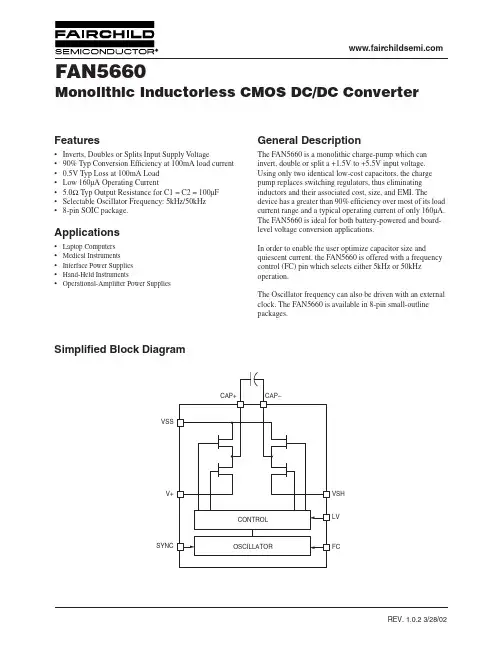
NCP5663DSADJR4G中文资料
- 格式:pdf
- 大小:383.75 KB
- 文档页数:12
Applications
• Servers • ASIC Power Supplies • Post Regulation for Power Supplies • Constant Current Source • Networking Equipment • Gaming and STB Modules
ABSOLUTE MAXIMUM RATINGS
Rating
Symbol
Value
Unit
Input Voltage
Vin
18
V
Output Pin Voltage
Vout
−0.3 to Vin +0.3
V
Adjust Pin Voltage
Vadj
−0.3 to Vin +0.3
V
Enable Pin Voltage
MARKING DIAGRAM
1 5
D2PAK CASE 936AA
NC P5663DSy AWYYWWG
1
Tab = Ground Pin 1. Enable
2. Vin 3. Ground 4. Vout 5. Adj (adjustable output) 5. Error Flag (fixed output)
Internal Current Limitation
Ripple Rejection (120 Hz) Ripple Rejection (1 kHz)
Vin Vn Vout
Iadj REGline REGload
VDO Iout Ilim RR
2.0 −
−1% −1.5% −2%
− − − − 3.0 − − −
− 28
− 0.9 −
40 0.03 0.03 1.0
− 4.5 70 65
9.0 −
+1% +1.5% +2%
− − − 1.3 − − − −
V mVrms
V
nA % % V A A dB
Thermal Shutdown (Guaranteed by Design)
TSHD
−
160
−
°C
Ground Current
元器件交易网
NCP5663
Low Output Voltage, Ultra−Fast 3.0 A Low Dropout Linear Regulator with Enable
The NCP5663 is a high performance, low dropout linear regulator designed for high power applications that require up to 3.0 A current. It is offered in both fixed and adjustable output versions. With output voltages as low as 0.9 V and ultra−fast response times for load transients, the NCP5663 also provides additional features such as Enable and Error Flag (for the fixed output version), increasing the utility of this device. A thermally robust, 5 pin D2Pak, combined with an architecture that offers low ground current (independent of load), provides for a superior high−current LDO solution.
Adjustable Pin Input Current
Line Regulation (Iout = 10 mA, Vout+1.5 V < Vin < 7.0 V) Load Regulation (10 mA < Iout < 3.0 A) Dropout Voltage (Iout = 3.0 A) Peak Output Current Limit
Human Body Model (HBM) JESD 22−A114−B
Machine Model (MM) JESD 22−A115−A.
The maximum package power dissipation is:
TJ(max) * TA
PD +
RqJA
The bipolar process employed for this IC is fully characterized and rated for reliable 18 V VCCmax operation. To avoid damaging the part or degrading it’s reliability, power dissipation transients should be limited to under 30 W for D2PAK.
Iout = 3.0 A
Iq
−
1.3
3.0
mA
Disabled State
Iqds
−
10
300
mA
Enable Input Threshold Voltage
Ven
V
Voltage Increasing, On state, Logic High
1.3
−
−
Voltage Decreasing, Off state, Logic Low
−
−
0.3
Enable Input Current
Ien
Enable Pin Voltage = 0.3 Vmax
Features
• Ultra−Fast Transient Response (Settling Time: 1−3 ms) • Low Noise Without Bypass Capacitor (28 mVrms) • Low Ground Current Independent of Load (3.0 mA Maximum) • Fixed/Adjustable Output Voltage Versions • Enable Function • Error Flag (Fixed Output Version) • Current Limit Protection • Thermal Protection • 0.9 V Reference Voltage for Ultra−Low Output Operation • Power Supply Rejection Ratio > 65 dB • This is a Pb−Free Device
(Adjustable Version)
5
Error Flag
An Error Flag is triggered when the output voltage is out of regulation excluding transient signals
(Fixed Version) that may occur. Requires a pullup resistor f 100 kW.
y = A for Adjustable Version B for Fixed 1.5 V Version
A = Assembly Location W = Wafer Lot Y = Year WW = Work Week G = Pb−Free
ORDERING INFORMATION
See detailed ordering and shipping information in the package dimensions section on page 11 of this data sheet.
Characteristic
Symbol
Min
Typ
Max
Unit
ADJUSTABLE OUTPUT VERSION
Input Voltage
Output Noise Voltage
Output Voltage Accuracy TJ = 25°C (Vin = Vout +1.5 V to 7.0 V, Iout = 10 mA to 3.0 A) TJ = −20 to +125°C (Vin = Vout +1.5 V to 7.0 V, Iout = 10 mA to 3.0 A) TJ = −40 to +150°C (Vin = Vout +1.5 V to 7.0 V, Iout = 10 mA to 3.0 A)
Pin Adj/Fixed
Pin Name
Description
1
Enable
This pin allows for on/off control of the regulator. To disable the device, connect to Ground. If this
function is not in use, connect to Vin.
For open−circuit to short−circuit transient,
PDTransient = VCCmax * ISC.
2
元器件交易网
NCP5663
ELECTRICAL CHARACTERISTICS (Vin − Vout = 1.5 V, for typical values TJ = 25°C, for min/max values TJ = −40°C to 85°C, Cin = Cout = 150 mF unless otherwise noted.)
• Servers • ASIC Power Supplies • Post Regulation for Power Supplies • Constant Current Source • Networking Equipment • Gaming and STB Modules
ABSOLUTE MAXIMUM RATINGS
Rating
Symbol
Value
Unit
Input Voltage
Vin
18
V
Output Pin Voltage
Vout
−0.3 to Vin +0.3
V
Adjust Pin Voltage
Vadj
−0.3 to Vin +0.3
V
Enable Pin Voltage
MARKING DIAGRAM
1 5
D2PAK CASE 936AA
NC P5663DSy AWYYWWG
1
Tab = Ground Pin 1. Enable
2. Vin 3. Ground 4. Vout 5. Adj (adjustable output) 5. Error Flag (fixed output)
Internal Current Limitation
Ripple Rejection (120 Hz) Ripple Rejection (1 kHz)
Vin Vn Vout
Iadj REGline REGload
VDO Iout Ilim RR
2.0 −
−1% −1.5% −2%
− − − − 3.0 − − −
− 28
− 0.9 −
40 0.03 0.03 1.0
− 4.5 70 65
9.0 −
+1% +1.5% +2%
− − − 1.3 − − − −
V mVrms
V
nA % % V A A dB
Thermal Shutdown (Guaranteed by Design)
TSHD
−
160
−
°C
Ground Current
元器件交易网
NCP5663
Low Output Voltage, Ultra−Fast 3.0 A Low Dropout Linear Regulator with Enable
The NCP5663 is a high performance, low dropout linear regulator designed for high power applications that require up to 3.0 A current. It is offered in both fixed and adjustable output versions. With output voltages as low as 0.9 V and ultra−fast response times for load transients, the NCP5663 also provides additional features such as Enable and Error Flag (for the fixed output version), increasing the utility of this device. A thermally robust, 5 pin D2Pak, combined with an architecture that offers low ground current (independent of load), provides for a superior high−current LDO solution.
Adjustable Pin Input Current
Line Regulation (Iout = 10 mA, Vout+1.5 V < Vin < 7.0 V) Load Regulation (10 mA < Iout < 3.0 A) Dropout Voltage (Iout = 3.0 A) Peak Output Current Limit
Human Body Model (HBM) JESD 22−A114−B
Machine Model (MM) JESD 22−A115−A.
The maximum package power dissipation is:
TJ(max) * TA
PD +
RqJA
The bipolar process employed for this IC is fully characterized and rated for reliable 18 V VCCmax operation. To avoid damaging the part or degrading it’s reliability, power dissipation transients should be limited to under 30 W for D2PAK.
Iout = 3.0 A
Iq
−
1.3
3.0
mA
Disabled State
Iqds
−
10
300
mA
Enable Input Threshold Voltage
Ven
V
Voltage Increasing, On state, Logic High
1.3
−
−
Voltage Decreasing, Off state, Logic Low
−
−
0.3
Enable Input Current
Ien
Enable Pin Voltage = 0.3 Vmax
Features
• Ultra−Fast Transient Response (Settling Time: 1−3 ms) • Low Noise Without Bypass Capacitor (28 mVrms) • Low Ground Current Independent of Load (3.0 mA Maximum) • Fixed/Adjustable Output Voltage Versions • Enable Function • Error Flag (Fixed Output Version) • Current Limit Protection • Thermal Protection • 0.9 V Reference Voltage for Ultra−Low Output Operation • Power Supply Rejection Ratio > 65 dB • This is a Pb−Free Device
(Adjustable Version)
5
Error Flag
An Error Flag is triggered when the output voltage is out of regulation excluding transient signals
(Fixed Version) that may occur. Requires a pullup resistor f 100 kW.
y = A for Adjustable Version B for Fixed 1.5 V Version
A = Assembly Location W = Wafer Lot Y = Year WW = Work Week G = Pb−Free
ORDERING INFORMATION
See detailed ordering and shipping information in the package dimensions section on page 11 of this data sheet.
Characteristic
Symbol
Min
Typ
Max
Unit
ADJUSTABLE OUTPUT VERSION
Input Voltage
Output Noise Voltage
Output Voltage Accuracy TJ = 25°C (Vin = Vout +1.5 V to 7.0 V, Iout = 10 mA to 3.0 A) TJ = −20 to +125°C (Vin = Vout +1.5 V to 7.0 V, Iout = 10 mA to 3.0 A) TJ = −40 to +150°C (Vin = Vout +1.5 V to 7.0 V, Iout = 10 mA to 3.0 A)
Pin Adj/Fixed
Pin Name
Description
1
Enable
This pin allows for on/off control of the regulator. To disable the device, connect to Ground. If this
function is not in use, connect to Vin.
For open−circuit to short−circuit transient,
PDTransient = VCCmax * ISC.
2
元器件交易网
NCP5663
ELECTRICAL CHARACTERISTICS (Vin − Vout = 1.5 V, for typical values TJ = 25°C, for min/max values TJ = −40°C to 85°C, Cin = Cout = 150 mF unless otherwise noted.)