RC1117S285T中文资料
- 格式:pdf
- 大小:51.29 KB
- 文档页数:9
元器件交易网
元器件交易网
PRODUCT SPECIFICATION RC1117
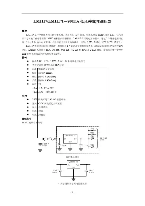
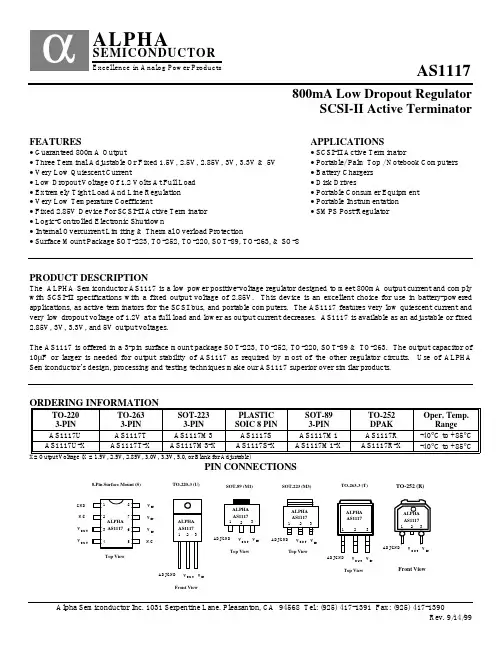
Pin Assignments
*With package soldered to 0.5 square inch copper area over backside ground plane or internal power plane., ΘJA can vary from
30°C/W to more than 50°C/W. Other mounting techniques may provide better thermal resistance than 30°C/W.
Absolute Maximum Ratings
Parameter Min.Max.Unit
V IN7.5V
Operating Junction Temperature Range0125°C
Storage Temperature Range-65150°C
Lead Temperature (Soldering, 10 sec.)300°C
RC1117PRODUCT SPECIFICATION
Electrical Characteristics
Operating Conditions: V IN ≤ 7V , T J = 25°C unless otherwise speci fied.
The • denotes speci fications which apply over the speci fied operating temperature range.
Notes:
1.See thermal regulation specifications for changes in output voltage due to heating effects. Load and line regulation are
measured at a constant junction temperature by low duty cycle pulse testing.
2.Line and load regulation are guaranteed up to the maximum power dissipation (18W). Power dissipation is determined by
input/output differential and the output current. Guaranteed maximum output power will not be available over the full input/output voltage range.3.RC1117 only.
Parameter
Conditions
Min.Typ.Max.Units Reference Voltage, V REF 3 1.5V ≤ (V IN - V OUT ) ≤ 5.75V, 10mA ≤ I OUT ≤ 1A
•
1.225(-2%) 1.250
1.275(+2%)V
Output Voltage
10mA ≤ I OUT ≤ 1A
RC1117-2.5, 4V ≤ V IN ≤ 7V RC1117-2.85, 4.35V ≤ V IN ≤ 7V RC1117-3.3, 4.8V ≤ V IN ≤ 7V RC1117-5, 6.5V ≤ V IN ≤ 7V
•••• 2.4502.7933.2344.900
2.52.85
3.35.0 2.5502.9073.3665.100V V V V Line Regulation 1,2 (V OUT + 1.5V) ≤ V IN ≤ 7V, I OUT = 10mA • 0.0050.2%Load Regulation 1,2 (V IN – V OUT ) = 2V, 10mA ≤ I OUT ≤ 1A • 0.050.5%Dropout Voltage ∆ V REF = 1%, I OUT = 1A • 1.100
1.200V Current Limit
(V IN – V OUT ) = 2V
• 1.1 1.5A Adjust Pin Current, I Adj 3 • 35120 µ A Adjust Pin Current Change 3 1.5V ≤ (V IN – V OUT ) ≤ 5.75,10mA ≤ I OUT ≤ 1A • 0.2
5
µ A Minimum Load Current 1.5V ≤ (V IN – V OUT ) ≤ 5.75 • 10
mA
Quiescent Current V IN = V OUT + 1.25V
•
4
13
mA Ripple Rejection f = 120Hz, C OUT = 22 µ F Tantalum, (V IN – V OUT ) = 3V, I OUT = 1A 60
72dB Thermal Regulation T A = 25 ° C, 30ms pulse
0.0040.02%/W Temperature Stability •
0.5%Long-Term Stability T A = 125 ° C, 1000hrs.0.03 1.0%RMS Output Noise (% of V OUT )
T A = 25 ° C, 10Hz ≤ f ≤ 10kHz
0.003%Thermal Resistance, Junction to Case SOT-22315 ° C/W TO-252, TO-2633 ° C/W Thermal Shutdown Junction Temperature
155 ° C Thermal Shutdown Hysteresis
10
°
C
元器件交易网
元器件交易网
PRODUCT SPECIFICATION RC1117
Typical Performance Characteristics
Figure 5. Minimum Load Current vs. Temperature Figure 6. Adjust Pin Current vs. Temperature
RC1117PRODUCT SPECIFICATION
PRODUCT SPECIFICATION RC1117 Mechanical Dimensions
4-Lead SOT-223 Package
RC1117PRODUCT SPECIFICATION
LIFE SUPPORT POLICY
FAIRCHILD ’S PRODUCTS ARE NOT AUTHORIZED FOR USE AS CRITICAL COMPONENTS IN LIFE SUPPORT DEVICES OR SYSTEMS WITHOUT THE EXPRESS WRITTEN APPROVAL OF THE PRESIDENT OF FAIRCHILD SEMICONDUCTOR CORPORATION. As used herein:
1.Life support devices or systems are devices or systems
which, (a) are intended for surgical implant into the body,or (b) support or sustain life, and (c) whose failure to perform when properly used in accordance with instructions for use provided in the labeling, can be
reasonably expected to result in a significant injury of the user. 2. A critical component in any component of a life support
device or system whose failure to perform can be
reasonably expected to cause the failure of the life support device or system, or to affect its safety or effectiveness.
DISCLAIMER
FAIRCHILD SEMICONDUCTOR RESERVES THE RIGHT TO MAKE CHANGES WITHOUT FURTHER NOTICE TO ANY PRODUCTS HEREIN TO IMPROVE RELIABILITY, FUNCTION OR DESIGN. FAIRCHILD DOES NOT ASSUME
ANY LIABILITY ARISING OUT OF THE APPLICATION OR USE OF ANY PRODUCT OR CIRCUIT DESCRIBED HEREIN; NEITHER DOES IT CONVEY ANY LICENSE UNDER ITS PATENT RIGHTS, NOR THE RIGHTS OF OTHERS.。