英文文献和中文翻译、单片机控制在梭式窑中的应用
- 格式:doc
- 大小:85.50 KB
- 文档页数:14
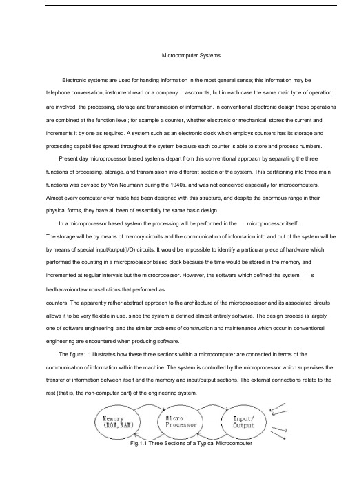
Microcomputer SystemsElectronic systems are used for handing information in the most general sense; this information may be telephone conversation, instrument read or a company ' asccounts, but in each case the same main type of operation are involved: the processing, storage and transmission of information. in conventional electronic design these operations are combined at the function level; for example a counter, whether electronic or mechanical, stores the current and increments it by one as required. A system such as an electronic clock which employs counters has its storage and processing capabilities spread throughout the system because each counter is able to store and process numbers.Present day microprocessor based systems depart from this conventional approach by separating the three functions of processing, storage, and transmission into different section of the system. This partitioning into three main functions was devised by Von Neumann during the 1940s, and was not conceived especially for microcomputers. Almost every computer ever made has been designed with this structure, and despite the enormous range in their physical forms, they have all been of essentially the same basic design.In a microprocessor based system the processing will be performed in the microprocessor itself.The storage will be by means of memory circuits and the communication of information into and out of the system will be by means of special input/output(I/O) circuits. It would be impossible to identify a particular piece of hardware which performed the counting in a microprocessor based clock because the time would be stored in the memory and incremented at regular intervals but the microprocessor. However, the software which defined the system ' s bedhacvoionrtawinousel ctions that performed ascounters. The apparently rather abstract approach to the architecture of the microprocessor and its associated circuits allows it to be very flexible in use, since the system is defined almost entirely software. The design process is largely one of software engineering, and the similar problems of construction and maintenance which occur in conventional engineering are encountered when producing software.The figure1.1 illustrates how these three sections within a microcomputer are connected in terms of the communication of information within the machine. The system is controlled by the microprocessor which supervises the transfer of information between itself and the memory and input/output sections. The external connections relate to the rest (that is, the non-computer part) of the engineering system.Fig.1.1 Three Sections of a Typical MicrocomputerAlthough only one storage sect ion has bee n show n in the diagram, in practice two dist inct types of memory RAM and ROM are used. In each case, the word ‘ memory' rather in appropriate since a computers memory is more like a filing cabinet in concept; information is stored in a set of numbered‘ boxes ' and it is referenced by the serial number ohe ‘ box ' in question.Microcomputers use RAM (Random Access Memory) into which data can be written and from which data can be read again when needed. This data can be read back from the memory in any sequence desired, and not necessarily the same order in which it was written, hence the expression ‘ ran dom ' access memory. Ano tltype of ROM (Read Only Memory) is used to hold fixed patter ns of in formatio n which cannot be affected by the microprocessor; these patter ns are n ot lost whe n power is removed and are normally used to hold the program which defines the behavior of a microprocessor based system. ROMs can be read like RAMs, but un like RAMs they cannot be used to store variable in formati on. Some ROMs have their data patter ns put in duri ng manufacture, while others are programmable by the user by means of special equipment and are called programmable ROMs. The widely used programmable ROMs are erasable by means of special ultraviolet lamps and are referred to as EPROMs, short for Erasable Programmable Read Only Memories. Other new types of device can be erased electrically without the need for ultraviolet light, which are called Electrically Erasable Programmable Read Only Memories, EEPROMs.The microprocessor processes data under the control of the program, controlling the flow of information to and from memory and input/output devices. Some input/output devices are gen eral-purpose types while others are desig ned for con troll ing special hardware such as disc drives or con troll ing in formatio n tran smissi on to other computers. Most types of I/O devices are programmable to some extent, allowing different modes of operation, while some actually contain special-purpose microprocessors to permit quite complex operations to be carried out without directly involving the main microprocessor.The microprocessor processes data under the control of the program, controlling the flow of information to and from memory and input/output devices. Some input/output devices are general-purpose types while others are designed for controlling special hardware such as disc drives or controlling information transmission to other computers. Most types of I/O devices are programmable to some extent, allowing different modes of operation, while some actually contain special-purpose microprocessors to permit quite complex operations to be carried out without directly involving the main microprocessor.The microprocessor , memory and input/output circuit may all be contained on the same integrated circuit provided that the application does not require too much program or data storage . This is usually the case in low-cost application such as the controllers used in microwave ovens and automatic washing machines . The use of single package allows considerable cost savings to e made when articles are manufactured in large quantities . As technology develops , moreand more powerful processors and larger and larger amounts of memory are being incorporated into single chip microcomputers with resulting saving in assembly costs in the final products . For the foreseeable future , however , it will continue to be necessary to interconnect a number of integrated circuits to make a microcomputer whenever larger amounts of storage or input/output are required.Another major engineering application of microcomputers is in process control. Here the presence of the microcomputer is usually more apparent to the user because provision is normally made for programming the microcomputer for the particular application. In process control applications the benefits lf fitting the entire system on to single chip are usually outweighed by the high design cost involved, because this sort lf equipment is produced in smaller quantities. Moreover, process controllers are usually more complicated so that it is more difficult to make them as single integrated circuits. Two approaches are possible; the controller can be implemented as a general-purpose microcomputer rather like a more robust version lf a hobby computer, or as a ‘ packageds'ystem, signed for replacing controllers based on older technologies such as electromagnetic relays. In the former case the system would probably be programmed in conventional programming languages such as the ones to9 be introduced later, while in the other case a special-purpose language might be used, for example one which allowed the function of the controller to be described in terms of relay interconnections, In either case programs can be stored in RAM, which allows them to be altered to suit changes in application, but this makes the overall system vulnerable to loss lf power unless batteries are used to ensure continuity of supply. Alternatively programs can be stored in ROM, in which case they virtually become part of the electronic ‘ hardwarean'd are often referred to as firmware. More sophisticated process controllersrequire minicomputers for their implementation, although the use lf large scale integrated circuits distinction between mini and microcomputers, Products and process controllers of various kinds represent the majority of present-day microcomputer applications, the exact figures depending on one ' s interpretation of the word ‘ product ' . Virtually all engineering and scientific uses of microcomputers can be assigned to one or other of these categories. But in the system we most study Pressure and Pressure Transmitters. Pressure arises when a force is applied over an area. Provided the force is one Newton and uniformly over the area of one square meters, the pressure has been designated one Pascal.Pressure is a universal processing condition. It is also a condition of life on the planet: we live at the bottom of an atmospheric ocean that extends upward for many miles. This mass of air has weight, and this weight pressing downward causes atmospheric pressure. Water, a fundamental necessity of life, is supplied to most of us under pressure. In the typical process plant, pressure influences boiling point temperatures, condensing point temperatures, process efficiency, costs, and other important factors. The measurement and control of pressure or lack of it-vacuum-in the typical process plant is critical.The working instruments in the plant usually include simple pressure gauges, precision recorders and indicators, and pneumatic and electronic pressure transmitters. A pressure transmitter makes a pressure measurement and generates either a pneumatic or electrical signal output that is proportional to the pressure being sensed.In the process plant, it is impractical to locate the control instruments out in the place near the process. It is also true that most measurements are not easily transmitted from some remote location. Pressure measurement is an exception, but if a high pressure of some dangerous chemical is to be indicated or recorded several hundred feet from the point of measurement, a hazard may be from the pressure or from the chemical carried.To eliminate this problem, a signal transmission system was developed. This system is usually either pneumatic or electrical. And control instruments in one location. This makes it practical for a minimum number of operators to run the plant efficiently.When a pneumatic transmission system is employed, the measurement signal is converted into pneumatic signal by the transmitter scaled from 0 to 100 percent of the measurement value. This transmitter is mounted close to the point of measurement in the process. The transmitter output-air pressure for a pneumatic transmitter-is piped to the recording or control instrument. The standard output range for a pneumatic transmitter is 20 to 100kPa, which is almost universally used.When an electronic pressure transmitter is used, the pressure is converted to electrical signal that may be current or voltage. Its standard range is from 4 to 20mA DC for current signal or from 1 to 5V DC for voltage sig nal. Nowadays, ano ther type of electrical sig nal, which is beco ming com mon, is the digital or discrete signal. The use of instruments and control systems based on computer or forcing in creased use of this type of sig nal.Sometimes it is importa nt for an alysis to obtai n the parameters that describe the sen sor/tra nsmitter behavior. The gain is fairly simple to obta in once the spa n is known. Con sider an electr onic pressure transmitter with a range of 0 〜600kPa.The gain is… 20mA 4mA 16mA 小“ mAKr 0.027——600kPa 0kPa 600kPa kPadefi ned as the cha nge in output divided by the cha nge in in put. In this case, the output is electrical sig nal (4 〜20mA DC) and the in put is process pressure (0 〜600kPa). Thus the gain. Beside we mustmeasure Temperature Temperature measureme nt is importa nt in in dustrial con trol, as direct in dicati ons of system or product state and as in direct in dicati ons of such factors as react ion rates, en ergy flow, turbine efficie ncy, and lubrica nt quality. Prese nt temperature scales have bee n in use for about 200 years, the earliest in strume nts were based on the thermal expa nsion of gases and liquids. Such filled systems are still employed, although many other types of in strume nts are available. Represe ntative temperature sen sors in clude: filled thermal systems, liquid-i n-glassthermometers, thermocouples, resista nee temperature detectors, thermostats, bimetallic devices, optical and radiati on pyrometers and temperature-se nsitive pain ts.Adva ntages of electrical systems in clude high accuracy and sen sitivity, practicality of switch ing or scanning several measurements points, larger distances possible between measuring elements and controllers, replacement of components(rather than complete system), fast response, and ability to measure higher temperature. Among the electrical temperature sen sors, thermocouples and resista nee temperature detectors are most widely used.Descriptio nThe AT89C51 is a low-power, high-performa nee CMOS 8-bit microcomputer with 4K bytes of Flash programmable and erasable read only memory (PEROM). The device is manufactured using Atmel ' shigh-de nsity non volatile memory tech no logy and is compatible with the in dustry-sta ndard MCS-51 instruction set and pinout. The on-chip Flash allows the program memory to be reprogrammed in-system or by a conven tio nal non volatile memory programmer. By comb ining a versatile 8-bit CPU with Flash on a monolithic chip, the Atmel AT89C51 is a powerful microcomputer which provides a highly-flexible and cost-effective solution to many embedded control applications.Function characteristicThe A T89C51 provides the following standard features: 4K bytes of Flash, 128 bytes of RAM, 32 I/O lines, two 16-bit timer/counters, a five vector two-level interrupt architecture, a full duplex serial port, on-chip oscillator and clock circuitry. In addition, the AT89C51 is designed with static logic for operation down to zero frequency and supports two software selectable power saving modes. The Idle Mode stops the CPU while allowing the RAM, timer/counters, serial port and interrupt system to continue functioning. The Power-down Mode saves the RAM contents but freezes the oscillator disabling all other chip functions until the next hardware reset.Pin DescriptionVCC :Supply voltage.GND :Ground.Port 0 :Port 0 is an 8-bit open-drain bi-directional I/O port. As an output port, each pin can sink eight TTL inputs. When 1s are written to port 0 pins, the pins can be used as highimpedance inputs.Port 0 may also be configured to be the multiplexed loworder address/data bus during accesses to external program and data memory. In this mode P0 has internal pullups.Port 0 also receives the code bytes during Flash programming,and outputs the code bytes during programverification. External pullups are required during programverification.Port 1Port 1 is an 8-bit bi-directional I/O port with internal pullups.The Port 1 output buffers can sink/source four TTLinputs.When 1s are written to Port 1 pins they are pulled high by the internal pullups and can be used as inputs. As inputs,Port 1 pins that are externally being pulled low will source current (IIL) because of the internal pullups.Port 1 also receives the low-order address bytes during Flash programming and verification.Port 2Port 2 is an 8-bit bi-directional I/O port with internal pullups.The Port 2 output buffers can sink/source four TTLinputs.When 1s are written to Port 2 pins they are pulled high by the internal pullups and canbe used as inputs. As inputs,Port 2 pins that are externally being pulled low will source current, because of the internal pullups.Port 2 emits the high-order address byte during fetches from external program memory and during accesses to external data memory that use 16-bit addresses. In this application, it uses strong internal pullupswhen emitting 1s. During accesses to external data memory that use 8-bitaddresses, Port 2 emits the contents of the P2 Special Function Register.Port 2 also receives the high-order address bits and some control signals during Flash programming and verification.Port 3Port 3 is an 8-bit bi-directional I/O port with internal pullups.The Port 3 output buffers can sink/source four TTLinputs.When 1s are written to Port 3 pins they are pulled high by the internal pullups and can be used as inputs. As inputs,Port 3 pins that are externally being pulled low will source current (IIL) because of the pullups.Port 3 also serves the functions of various special features of the AT89C51 as listed below:Port 3 also receives some control signals for Flash programming and verification.RSTReset input. A high on this pin for two machine cycles while the oscillator is running resets the device. ALE/PROG Address Latch Enable output pulse for latching the low byte of the address during accesses to external memory. This pin is also the program pulse input (PROG) during Flash programming.In normal operation ALE is emitted at a constant rate of 1/6 the oscillator frequency, and may be used for external timing or clocking purposes. Note, however, that one ALE pulse is skipped during each access to external Data Memory.If desired, ALE operation can be disabled by setting bit 0 of SFR location 8EH. With the bit set, ALE is active only during a MOVX or MOVC instruction. Otherwise, the pin is weakly pulled high. Setting the ALE-disable bit has no effect if the microcontroller is in external execution mode.PSENProgram Store Enable is the read strobe to external program memory.When the AT89C51 is executing code from external program memory, PSEN is activated twice each machine cycle, except that two PSEN activations are skipped during each access to external data memory.EA/VPPExternal Access Enable. EA must be strapped to GND in order to enable the device to fetch code from external program memory locations starting at 0000H up to FFFFH. Note, however, that if lock bit 1 is programmed, EA will be internally latched on reset.EA should be strapped to VCC for internal program executions.This pin also receives the 12-volt programming enable voltage(VPP) during Flash programming, for parts that require12-volt VPP.XTAL1Input to the inverting oscillator amplifier and input to the internal clock operating circuit.XTAL2Output from the inverting oscillator amplifier.Oscillator CharacteristicsXTAL1 and XTAL2 are the input and output, respectively,of an inverting amplifier which can be configured for use as an on-chip oscillator, as shown in Figure 1.Either a quartz crystal or ceramic resonator may be used. To drive the device from an external clock source, XTAL2 should be left unconnected while XTAL1 is driven as shown in Figure 2.There are no requirements on the duty cycle of the external clock signal, since the input to the internal clocking circuitry is through a divide-by-two flip-flop, but minimum and maximum voltage high and low time specifications must be observed.微型计算机控制系统(单片机控制系统)广义地说,微型计算机控制系统(单片机控制系统)是用于处理信息的,这种被用于处理的信息可以是电话交谈,也可以是仪器的读数或者是一个企业的帐户,但是各种情况下都涉及到相同的主要操作:信息的处理、信息的存储和信息的传递。
The series SCM of AT891.1 AT89C511.Features●4K Bytes of In-System Reprogrammable Flash Memory– Endurance: 1,000 Write/Erase Cycles●Three-level Program Memory Lock●128 x 8-bit Internal RAM●32 Programmable I/O Lines●Two 16-bit Timer/Counters●Six Interrupt Sources●Low-power Idle and Power-down Modes2.DescriptionThe AT89C51 is a low-power, high-performance CMOS 8-bit microcomputer with 4Kbytes of Flash programmable and erasable read only memory (PEROM). The device is manufactured using Atmel’s high-density nonvolatile memory technology and is compatible with the industry-standard MCS-51 instruction set and pinout. The on-chip Flash allows the program memory to be reprogrammed in-system or by a conventional nonvolatile memory programmer. By combining a versatile 8-bit CPU with Flash on a monolithic chip, the Atmel AT89C51 is a powerful microcomputer which provides a highly-flexible and cost-effective.3.Pin Configurations4Pin DescriptionVCC—Supply voltage.GND—Ground.Figure A1Port 0Port 0 is an 8-bit open-drain bi-directional I/O port. As an output port, each pin can sink eight TTL inputs. When 1s are written to port 0 pins, the pins can be used as high-impedance inputs. Port 0 may also be configured to be the multiplexed low-order address/data bus during accesses to external program and data memory. In this mode P0 has internal pullups. Port 0 also receives the code bytes during Flash programming, and outputs the code bytes during program verification. External pullups are required during program verification.Port 1Port 1 is an 8-bit bi-directional I/O port with internal pullups. The Port 1 output buffers can sink/source four TTL inputs. When 1s are written to Port 1 pins they are pulled high by the internal pullups and can be used as inputs. As inputs, Port 1 pins that are externally being pulled low will source current (TTL) because of the internal pullups. Port 1 also receives the low-order address bytes during Flash programming and verification.Port 2Port 2 is an 8-bit bi-directional I/O port with internal pullups. The Port 2 output buffers can sink/source four TTL inputs. When 1s are written to Port 2 pins they arepulled high by the internal pullups and can be used as inputs. As inputs, Port 2 pins that are externally being pulled low will source current (TTL) because of the internal pullups. Port 2 emits the high-order address byte during fetches from external program memory and during accesses to external data memory that use 16-bit addresses (MOVX @DPTR). In this application, it uses strong internal pullups when emitting 1s. During accesses to external data memory that use 8-bit addresses (MOVX @ RI), Port 2 emits the contents of the P2 Special Function Register. Port 2 also receives the high-order address bits and some control signals during Flash programming and verification.Port 3Port 3 is an 8-bit bi-directional I/O port with internal pullups. The Port 3 output buffers can sink/source four TTL inputs. When 1s are written to Port 3 pins they are pulled high by the internal pullups and can be used as inputs. As inputs, Port 3 pins that are externally being pulled low will source current (TTL) because of the pullups. Port 3 also serves the functions of various special features of the AT89C51 as listed below: Port 3 also receives some control signals for Flash programming and verification. RSTReset input. A high on this pin for two machine cycles while the oscillator is running resets the devicePSENProgram Store Enable is the read strobe to external program memory. When the AT89C51 is executing code from external program memory, PSEN is activated twice each machine cycle, except that two PSEN activations are skipped during each access to external data memory.ALE/PROGAddress Latch Enable output pulse for latching the low byte of the address during accesses to external memory. This pin is also the program pulse input (PROG) during Flash programming. In normal operation ALE is emitted at a constant rate of 1/6 theoscillator frequency, and may be used for external timing or clocking purposes. Note, however, that one ALE pulse is skipped during each access to external Data Memory. If desired, ALE operation can be disabled by setting bit 0 of SFR location 8EH. With the bit set, ALE is active only during a MOVX or MOVC instruction. Otherwise, the pin is weakly pulled high. Setting the ALE-disable bit has no effect if the microcontroller is in external execution mode.EA/VPPExternal Access Enable. EA must be strapped to GND in order to enable the device to fetch code from external program memory locations starting at 0000H up to FFFFH. Note, however, that if lock bit 1 is programmed, EA will be internally latched on reset. EA should be strapped to VCC for internal program executions. This pin also receives the 12-volt programming enable voltage (VPP) during Flash programming, for parts that require 12-volt VPP.XTAL1Input to the inverting oscillator amplifier and input to the internal clock operating circuit.XTAL2Output from the inverting oscillator amplifier.5.Oscillator CharacteristicsXTAL1 and XTAL2 are the input and output, respectively, of an inverting amplifier which can be configured for use as an on-chip oscillator, as shown in Figure 1. Either a quartz crystal or ceramic resonator may be used. To drive the device from an external clock source, XTAL2 should be left unconnected while XTAL1 is driven as shown in Figure 2. There are no requirements on the duty cycle of the external clock signal, since the input to the internal clocking circuitry is through a divide-by-two flip-flop, but minimum and maximum voltage high and low time specifications must be observed.6.Idle ModeIn idle mode, the CPU puts itself to sleep while all the onchip peripherals remain active. The mode is invoked by software. The content of the on-chip RAM and all the special functions registers remain unchanged during this mode. The idle mode can be terminated by any enabled interrupt or by a hardware reset. It should be noted that when idle is terminated by a hard ware reset, the device normally resumes program execution, from where it left off, up to two machine cycles before the internal reset algorithm takes control. On-chip hardware inhibits access to internal RAM in this event, but access to the port pins is not inhibited. To eliminate the possibility of an unexpected write to a port pin when Idle is terminated by reset, the instruction following the one that invokes Idle should not be one that writes to a port pin or to external memory.7.Power-down ModeIn the power-down mode, the oscillator is stopped, and the instruction that invokes power-down is the last instruction executed. The on-chip RAM and Special Function Registers retain their values until the power-down mode is terminated. The only exit from power-down is a hardware reset. Reset redefines the SFRs but does not change the on-chip RAM. The reset should not be activated before VCC is restored to its normal operating level and must be held active long enough to allow the oscillator to restart and stabilize.8.Program Memory Lock BitsOn the chip are three lock bits which can be left unprogrammed (U) or can be programmed (P) to obtain the additional features listed in the table below.9.Programming the FlashThe AT89C51 is normally shipped with the on-chip Flash memory array in the erased state (that is, contents = FFH) and ready to be programmed. The programming interface accepts either a high-voltage (12-volt) or a low-voltage (VCC) program enable signal. The low-voltage programming mode provides a convenient way to program the AT89C51 inside the user’s system, while the high-voltage programming mode iscompatible with conventional third party Flash or EPROM programmers. The AT89C51 is shipped with either the high-voltage or low-voltage programming mode enabled. The respective top-side marking and device signature codes are listed in the following table.The AT89C51 code memory array is programmed byte-bybyte in either programming mode. To program any nonblank byte in the on-chip Flash Memory, the entire memory must be erased using the Chip Erase Mode. Programming Algorithm: Before programming the AT89C51, the address, data and control signals should be set up according to the Flash programming mode table and Figure 3 and Figure 4. To program the AT89C51, take the following steps.(1)Input the desired memory location on the address lines.(2)Input the appropriate data byte on the data lines.(3)Activate the correct combination of control signals.(4)Raise EA/VPP to 12V for the high-voltage programming mode.(5)Pulse ALE/PROG once to program a byte in the Flash array or the lock bits. The byte-write cycle is self-timed and typically takes no more than 1.5 ms.(6)Repeat steps 1 through 5, changing the address and data for the entire array or until the end of the object file is reached.Data Polling:The AT89C51 features Data Polling to indiate the end of a write cycle. During a write cycle, an attempted read of the last byte written will result in the complement of the written datum on P0.7. Once the write cycle has been completed, true data are valid on all outputs, and the next cycle may begin. Data Polling may begin any time after a write cycle has been initiated.Ready/Busy: The progress of byte programming can also be monitored by the RDY/BSY output signal. P3.4 is pulled low after ALE goes high during programming to indicate BUSY. P3.4 is pulled high again when programming is done to indicate READY.Program Verify:If lock bits LB1 and LB2 have not been programmed, theprogrammed code data can be read back via the address and data lines for verification. The lock bits cannot be verified directly. Verification of the lock bits is achieved by observing that their features are enabled.Chip Erase:The entire Flash array is erased electrically by using the proper combination of control signals and by holding ALE/PROG low for 10 ms. The code array is written with all ―1‖s. The chip erase operation must be executed before the code memory can be re-programmed.Reading the Signature Bytes:The signature bytes are read by the same procedure as a normal verification of locations 030H, 031H, and 032H, except that P3.6 and P3.7 must be pulled to a logic low. The values returned are as follows.(030H) = 1EH indicates manufactured by Atmel(031H) = 51H indicates 89C51(032H) = FFH indicates 12V programming(032H) = 05H indicates 5V programming1.2 AT89C52The AT89C52 is a low-power, high-performance CMOS 8-bit microcomputer with 8K bytes of Flash programmable and erasable read only memory (PEROM). The device is manufactured using Atmel’s high-density nonvolatile memory technology and is compatible with the industry-standard 80C51 and 80C52 instruction set and pinout The on-chip Flash allows the program memory to be reprogrammed in-system or by a conventional nonvolatile memory programmer. By combining a versatile 8-bit CPU with Flash on a monolithic chip, the Atmel AT89C52 is a powerful microcomputer which provides a highly-flexible and cost-effective solution to many embedded control applications.The AT89C52 provides the following standard features: 8K bytes of Flash, 256 bytes of RAM, 32 I/O lines, three 16-bit timer/counters, a six-vector two-level interrupt architecture, a full-duplex serial port, on-chip oscillator, and clock circuitry. In addition,the AT89C52 is designed with static logic for operation down to zero frequency and supports two software selectable power saving modes. The Idle Mode serial port, and interrupt system to continue functioning. The Power-down mode saves the RAM contents but freezes the oscillator, disabling all other chip functions until the next hardware reset.Features:• Compatible with MCS-51™ Products• 8K Bytes of In-System Reprogrammable Flash Memory• Endurance: 1,000 Write/Erase Cycles• Fully Static Operation: 0 Hz to 24 MHz• Three-level Program Memory Lock• 256 x 8-bit Internal RAM• 32 Programmable I/O Lines• Three 16-bit Timer/Counters• Eight Interrupt Sources• Programmable Serial Channel• Low-power Idle and Power-down ModesPin Description:V CC: Supply voltageGND: GroundAT89 系列单片机1.1 AT89C511、特性⏹内含4KB的flash存储器,擦写次数1000次;⏹具有可编程的3级程序锁定器;⏹内含128字节的RAM;⏹具有32根可编程的I/O线;⏹具有2个16位可编程定时器;⏹具有6个中断源;⏹两种低功耗工作模式,即空闲模式和掉电模式;2、概述AT89C51是一种低功耗,高性能,采用CMOS工艺的8KB的可在线编程的Flash 存储器。

中英文对照外文翻译文献(文档含英文原文和中文翻译)原文:The Numerical Control Engine Bed TransformsHarvey B.M ackey First numerical control system development summary brief hi story and tendency.In 1946 the first electronic accounting machine was born the world,this indicated the humanity created has been possib le to strengthen and partially to replace the mental labor the tool. It with the humanity these which in the agricultu re, the industry society created only is strengthens the phy sical labor the tool to compare, got up the quantitive leap ,entered the information society for the humanity to laythe foundation.After 6 years, in 1952, computer technology applied to t he engine bed , the first numerical control engine bed were born in US. From this time on, the traditional engine bed has had the archery target change. Since nearly half centu ry, the numerical control system has experienced two stages and six generation of development.1.1 Numerical control (NC) stage (1952 ~ 1970)The early computer operating speed is low, was not big to then science computation and the data processing influence ,but could not adapt the engine bed real-time control reques t.The people can not but use numeral logic circuit "to buil d"to become an engine bed special purpose computer to take the numerical control system, is called the hardware connecti onnumerical control (HARD-WIRED NC), Jian Chengwei numerical c ontrol (NC). Along with the primary device development, this stage has had been through repeatedly three generations, na mely 1952 first generation of -- electron tube; 1959 second generation of -- transistor; 1965 third generation -- small scale integration electric circuit.1.2 Computer numerical control (CNC) stage (in 1970 ~ presen t)In 1970, the general minicomputer already appeared and th e mass production. Thereupon transplants it takes the numeric al control system the core part, from this time on entered the computer numerical control (CNC) the stage ("which should have computer in front of the general" two characters to ab breviate). In 1971, American INTEL Corporation in the world first time the computer two most cores part -- logic units and the controller, used the large scale integrated circuit technology integration on together the chip, called it the m icroprocessor (MICROPROCESSOR), also might be called the centr al processing element (to be called CPU).The microprocessor is applied to 1974 in the numerical c ontrol system. This is because minicomputer function too stro ng, controlled an engine bed ability to have wealthily (therefore once uses in controlling the multi- Taiwan engine bed at that time, called it group control), was inferior to use d the microprocessor economy to be reasonable. Moreover then small machine reliability was not ideal. The early microproce ssor speed and the function although insufficiently are also high, but may solve through the multi-processor structure. Because the microprocessor is the general-purpose calculator core part, therefore still was called the computer numerical control.In 1990, PC machine (personal computer, domestic custom had called microcomputer) the performance has developed tothe very high stage, may satisfiedly take the numerical cont rol system core part the request. Thenumerical control system henceforth entered based on the PC stage. In brief, the computer numerical control stage has also experienced three generations. Namely 1970 fourth generat ion of -- minicomputer; 1974 five dynasties -- microprocessor and 1990 sixth generation -- (overseas was called PC-BASED) based on PC.Also must point out, although overseas already renamed as the computer numerical control (namely CNC).Also must point out, although overseas already renamed as the computer numerical control (namely CNC), but our countr y still the custom called the numerical control (NC). Theref ore we daily say "numerical control", the materially already was refers to "computer numerical control".1.3 the numerical control future will develop tendency1.3.1 open style continues to, to develop based on the PC sixth generation of directionThe software and hardware resources has which based on P C are rich and so on the characteristic, the more numerical controls serial production factory can step onto this path. Uses PC machine to take at least its front end machine, pr ocesses the man-machine contact surface, the programming, the association .Question and so on net correspondence, undertakes the num erical control duty by the original system. PC machine has the friendly man-machine contact surface, will popularize to all numerical controls system. The long-distance communication, the long-distance diagnosis and the service will be more common.1.3.2 approaches and the high accuracy developmentThis is adapts the engine bed to be high speed and the high accuracy direction need to develop.1.3.3 develops to the intellectualized directionAlong with the artificial intelligence in the computer do mainunceasing seepage and the development, the numerical control system intellectualized degree unceasingly will enhance.(1) applies the adaptive control technologyThe numerical control system can examine in the process some important information, and the automatic control system related parameter, achieves the improvement system running sta tus the goal.(2) introduces the expert system instruction processingThe skilled worker and expert's experience, the processing general rule and the special rule store in the system, take the craft parameter database as the strut, the establishmenthas the artificial intelligence the expert system.(3)introduces the breakdown to diagnose the expert system(4) intellectualized numeral servo driveMay through the automatic diagnosis load, but the automat ic control parameter, causes the actuation system to obtain the best movement.Second, engine bed numerical control transformation necessi ty.2.1 microscopic looks at the transformation the necessityFrom on microscopic looked below that, the numerical cont rol engine bed has the prominent superiority compared to the traditional engine bed, moreover these superiority come from the computer might which the numerical control system contain s.2.1.1 may process the traditional engine bed cannot proce ss the curve, the curved surface and so on the complex com ponents.Because the computer has the excellent operation ability, may the instant accurately calculate each coordinate axis ins tant to be supposed the movement physiological load of exerc ise, therefore may turn round thesynthesis complex curve or the curved surface.2.1.2 may realize the processing automation, moreover is the flexible automation, thus the efficiency may enhance 3 ~ 7 times compared to the traditional engine bed.Because the computer has the memory and the memory prope rty, may the procedure which inputs remember and save, thenthe order which stipulated according to the procedure automat ic carries out, thus realization automation. The numerical co ntrol engine bed so long as replaces a procedure, may reali ze another work piece processing automation, thus causes the single unit and the small batch of production can automate, therefore is called has realized "flexible automation".2.1.3 processings components precision high, size dispersion d egree small, makes the assembly to be easy, no longer needs "to make repairs".2.1.4 may realize the multi- working procedures centralism, r educes the components in engine bed between frequent transpor ting.2.1.5 has auto-alarm, the automatic monitoring, automatic comp ensation and so on the many kinds of autonomy function, thu s may realize long time nobody to safeguard the processing.2.1.6 advantage which derives by above five.For example: Reduced worker's labor intensity, saved the labor force (a person to be possible to safeguard the multi - Taiwan engine bed), reduced the work clothes, reduced the new product trial manufacturing cycle and the production cycl e, might to the market demand make rapid reaction and so o n.Above these superiority are the predecessor cannot imagine, is an extremely significant breakthrough. In addition, the en gine bed numerical control carries out FMC (flexible manufact ure unit), FMS (flexible manufacture system) as well as CIMS (computer integration manufacture system) and so on the enter prise becoming an information based society transformation foundation. The numerical control technology already became the manufacturing industry automation the core technology and the foundation technology.2.2 great watches the transformation the necessityFrom on macroscopic looked that, the industry developed c ountry armed forces, the airplane weapon industry, in the en d of the 70's, at the beginning of the 80's started the l arge-scale application numerical control engine bed. Its essen ce is, uses the information technology to the traditional in dustry (including the armed forces, airplane weapon industry) carries on the technological transformations. Except that uses outside the numerical control engine bed, FMC, FMS in the m anufacture process, but also includes in the product developm ent carries out CAD, CAE, CAM, the hypothesized manufactureas well as carries out MIS in the production management (ma nagement information system), CIMS and so on. As well as in creases the information technology in its production product, including artificial intelligence and so on content. Because uses the information technology to the country foreign troops, the airplane weapon industry carries on the thorough transfor mation (to call it becoming an information based society), f inally causes them the product in the international military goods and in the goods for civilian use market the competit ive power greatly is the enhancement. But we in the informa tion technology transformation tradition industry aspect compar ed to the developed country to fall behind approximately for 20 years. Like in our country engine bed capacity, numerical control engine bed proportion (numerical control rate) to 199 5 only then 1.9%, but Japan has reached 20.8% in 1994, therefore every year has the massive mechanical and electrical products import. This also on from on macroscopic explained the engine bed numerical control transformation necessity. Tho rd, the numerical control transformation content and superiorl y lacks3.1 Transformation industry startingIn US, Japan and Germany and so on the developed countr y, their engine bed transforms took the new economical growt h profession, thrives abundantly, is occupying the golden age .As a result of the engine bed as well as the technical u nceasing progress, the engine bed transformation is "the eter nal" topic. Our country's engine bed transformation industry, also enters from the old profession to by the numerical c ontrol technology primarily new profession. In US, Japan, Ger many, have the broad market with the numerical control techn ological transformations engine bed and the production line, has formed the engine bed and the production line numerical control transformation new profession. In US, the engine be d transformation industry is called the engine bed regenerati on(Remanufacturing) industry. Is engaged in the regeneration ind ustry famous company to include: The Bertsche engineering fir m, the ayton engine bed company, Devlieg-Bullavd (are valuabl e) serves the group, the US equipment company and so on. T he American valuable company has set up the company in Chin a. In Japan, the engine bed transformation industry is calle d the engine bed to reequip (Retrofitting) industry. Is enga ged in the reequipment industry famous company to include: B ig indentation project group, hillock three mechanical companies, thousand substitute fields labor machine company, wild engineering firm, shore field engineering firm, mountain this engineering firm and so on. 3.2 Numerical control transformat ion contentThe engine bed and the production line numerical control transformation main content has following several points: First is extensively recovers the function, to the engine bed, the production line has the breakdown partially to carr y on the diagnosis and the restoration;Second is NC, the addend reveals the installment on the ordinary engine bed, or adds the numerical control system, transforms the NC engine bed, the CNC engine bed;Third is renovates, for increases the precision, the effi ciency and the automaticity, to the machinery, the electricit y partially carries on renovates, reassembles the processing to the machine part, extensively recovers the precision; Does not satisfy the production request to it the CNC system to carry on the renewal by newest CNC;Fourth is the technology renews or the technical innovati on, for enhances the performance or the scale, or in order to use the new craft, the new technology, carries on the b ig scale in the original foundation the technology to renew or the technical innovation, the great scope raises the leve l and the scale renewal transformation. The new electri cal system transforms after, how carries on the debugging as well as the determination reasonable approval standard, also is the technology preparatory work important link. The debugg ing work involves the machinery, the hydraulic pressure, the electricity, the control, and so on, therefore must carry onby the project person in charge, other personnel coordinate. The debugging step may conform to simplicity to numerous, fr om infancy to maturity, carries on from outside to in, afte r also may the partial overall situation, after first the s ubsystem the 3.3 The numerical control transformation superior ly lacks 3.3.1 reduced investment costs, the date of deliv ery are short With purchases the new engine bed to comp are, may save 60% ~ 80% expense generally, the transformatio n expense is low. Large-scale, the special engine bed especi ally is specially obvious. The common large-scale engine bed transforms, only spends the new engine bed purchase expense 1/3, the date of delivery is short. But some peculiar circu mstances, like the high speed main axle, the tray automatic switching unit manufacture and the installment too requires a lot of work, costs a great deal of money, often transforms the cost to enhance 2 ~ 3 times, with purchases the new engine bed to compare, only can economical invest about 50 %.3.3.2 machine capability stable are reliable, the structure i s limitedUses foundation and so on lathe bed, column all is heav y but the firm casting component, but is not that kind of welding component, after the transformation engine bed perform ance high, the quality is good, may take the new equipment continues to use many years. But receives the original mecha nism the limit, not suitably makes the unprecedented transfor mation. 3.3.3 familiar understood the equipment, is advantag eous for the operation serviceWhen purchases the new equipment, did not understand whether the new equipment can satisfy its processing request. Th e transformation then otherwise, may precisely calculate the engine bed the processing ability; Moreover, because many yea rs use, the operator already understood to the engine bed c haracteristic, uses and services the aspect to train the tim e in the operation short, effective is quick. The transforma tion engine bed as soon as installs, may realize the capaci ty load revolution. 3.3.4 may fully use the existing condi tionMay fully use the existing ground, does not need to lik e buys when the new equipment such to have reto construct the ground. 3.3.5 may use the newest control technology enhances the production equipment the automated level and the efficiency, improves the equipment quality and the scale, alters to the old engine bed now the horizontal engine bed. Fourth, numerical control system choiceWhen the numerical control system mainly has three kind of types, the transformation, should act according to the sp ecial details to carry on the choice.4.1 Step-by-steps the open system which the electrical ma chinery drivesThis system servo drive mainly is step-by-steps the elect rical machinery, the power step-by-steps the electrical machin ery, the battery solution pulse motor and so on. Entering s ends out which by the numerical control system for instructi on pulse, after the actuation electric circuit control and t he power enlargement, causes to step-by-step the electrical m achinery rotation, through gear vice- and ball bearing guide screw vice- actuation executive component. So long as the control command pulse quantity, the frequency as well as the circular telegram order, then may control the executive compo nent movement the displacement quantity, the speed and the h eading. This kind of system does not need the physical loca tion and the velocity feedback which obtains to the input e nd, therefore called it the open system, this system displac ement precision mainly decided in step-by-steps the electrical machinery angular displacement precision, transmission part and so on gear guide screw pitches the precision, therefore the system displacement precision is low.This system structure simple, debugging service convenient, work reliable, cost low, is easy to reequip successfully.4.2 The asynchronous motor or the direct current machine drive, diffraction grating survey feedback closed loop numer ical control system .This system and the open system difference is: Physical location feedback signal which by position detector set and so on the diffraction grating, induction synchromesh obtains, carries on the comparison as necessary with the given value, two interpolations enlargements and the transformation, the ac tuation implementing agency, by the speed which assigns turns towards the elimination deviation the direction movement, unti l assigns the position and the feedback physical location in terpolation is equal to the zero. The closed loop enters fo r the systemEnters for the system complex in the structure compared to the split-ring, the cost is also high, requests strictly to the environment room temperature. The design and the debu gging is all more difficult than the open system. But mayobtain compared to the split-ring enters for a system higher precision, quicker speed, actuation power bigger characteristic target. May act according to the product specification, decid ed whether uses this kind of system.4.3 The direct current servo electrical machinery drives, encoder feedback semi-closure link numerical control system .Half closed-loop system examination part installs in among passes in the moving parts, indirectly surveys the executive component the position. It only can compensate a system ring circuit interior part of part the error, therefore, its prec ision compared to closed-loop system precision low, but its structure and the debugging all compares the closed-loop syst em to be simple. In makes the angular displacement examinati on part and the speed examination part and the servo electr ical machinery time a whole then does not need to consider the position detector set installs the question.The current production numerical control system company fa ctory quite are many, overseas famous company like German SI EMENS Corporation,Japanese FANUC Corporation; Native corporation like China Mount Everest Corporation, Beijing astronautics eng ine bed numerical control system group company, Central China numerical control company and Shenyang upscale numerical contr ol country engineering research center.When choice numerical control system mainly is each kind of precision which the engine bed must achieve after the nu merical control transformation, actuates the electrical machine ry the power and user's request.Fifth in the numerical control transformation the mainmechanical part reequips the discussionA new numerical control engine bed, must achieve in the design that, Has the high static dynamic rigidity; Movement vice- between friction coefficient small, the transmission is ceaseless; The power is big; Is advantageous for the operati on and the service. When engine bed numerical control transf ormation should meet the above requirements as far as possib le. Cannot think the numerical control installment and the o rdinary engine bed connects in has met the numerical control engine bed requirements together, but also should carry on t he corresponding transformation to the major component to ena ble it to achieve the certain design request, can obtain th e anticipated transformation goal. 5.1 skids guide railSaid to the numerical control lathe that, the guide rail besides should have the conventional lathe guidance precision and the technology capability, but also must have good bears the friction, the attrition characteristic, and the reduction but sends the dead area because of the friction drag. At t he same time must have the enough rigidity, by reduces the guide rail to distort to processes the precision the influen ce, must have the reasonable guide rail protection and the lubrication.5.2 gearThe common engine bed gear mainly concentrates in the headstock and the gear box.In order to guarantee the transmission precision, on the numerical control engine bed uses the gear precision class i s all higher than the ordinary engine bed. Must be able to achieve the ceaseless transmissionin the structure, thus transforms time, the engine bed maingear must satisfy the numerical control engine bed the reque st, by guarantees the engine bed processing precision.5.3 skids the guide screw and the ball bearing guide screwThe guide screw transmission relates directly to the tran smission chain precision. The guide screw selects mainly is decided requests and drives the torque request in the job p recision. Is not used by job precision request Gao Shike skids the guide screw, but should inspect the original guide screw attrition situation, like the pitch error and the pitc h accumulative error as well as matches the nut gap. The o rdinary circumstances skid the guide screw to be supposed no t to be lower than 6 levels, the nut gap oversized then r eplaces the nut. Uses skids the guide screw relative ball b earing guide screw price to be low, but satisfies the pre cision high components processing with difficulty.The ball bearing guide screw rubs loses slightly, the ef ficiency is high, its transmission efficiency may above 90%; Precision high, the life is long; When start moment of forc e and movement the moment of force approaches, may reduce t he electrical machinery to start the moment of force. Theref ore may satisfiedly compare the high accuracy components proc essing request. 5.4 safe protectionThe effect must take the security as a premise. Transfor ms in the engine bed must take the corresponding measure ac cording to the actual situation, cuts noticeable. The ball b earing guide screw vice- is the precision part, when the wo rk must take strict precautions against the dust is speciall y the scrap and the hard sand grains enters the roller conveyer. On longitudinal guide screw also coca overall sheet i ron safety mask. The big carriage with skids two end surfac es which the guide rail contacts to have to seal, prevented absolutely the flinty granulated foreign matter enters the sl iding surface damage guide rail.Sixth, After the engine bed electrical system transformati on, to operates, the programmers inevitably brings the new r equest. Therefore ahead of time carries on new system knowle dge training to the operator and the programmers to be extr emely important, after otherwise will affect the transformatio n the engine bed rapid investment production. The training c ontent should include the new operation kneading board dispos ition, the function, the instruction meaning generally; New s ystem functional scope, application method and with old syste m difference; Maintenance maintenance request; Programming stan dard and automated programming and so on. The key point is makes, gets a good grasp of the operating manual and the p rogramming instruction booklet.the numerical control transforms se Transforms the scope according to each equipment differently, must beforehand desig n the connection partial transformations, if transforms comple tely, should design the electro-mechanical transformation conne ction, the operation kneading board control and the dispositi on, the interconnection partial contacts, the parameter measur ing point, services the position and so on, the request ope rates and services conveniently, reasonable, the line moves t owards, center the small junction smoothly few, the strong a nd the weak electrical noise is smallest, has the suitable allowance and so on. Partial transformation, but also needsto consider the new old system the performance match, the v oltage polarity and the size transformation, install the posi tion, the digital-analog conversion and so on, when the nece ssity must manufacture the transformation connection voluntaril y.veral examples1st, transforms the X53 milling machine with SIEMENS 810MIn 1998, the company invested 200,000 Yuan, with German Simens the 810M numerical control system, the 611A exchange servo drive system sds was the X53 milling machine carries on X, Y, the Z three axle numerical control transformation to a company's model; Retained the original main axle system and the cooling system; The transformation three axle has us ed the roller lead screw and the gear drive organization on the machinery. The entire transformation work including the m achine design, the electrical design, the PLC procedure estab lishment and the debugging, the engine bed overhaul, finally is the entire machine installment and the debugging. After t he milling machine transforms, processing effective stroke X/Y /The Z axis respectively is 88.0/270/28 billion mm; Maximum speed X/Y/The Z axis respectively is 5000/1500/800 mm/Min; Ma nual speed X/Y/The Z axis respectively is 3000/1000/500 mm/Mi n; The engine bed processing precision achieves ±0.001mm. The engine bed three coordinates linkage may complete each kind of complex curve or the curved surface processi ng.2nd, transforms the C6140 lathe with GSK980T and the exc hange servo drive system sds .In 2000, with Guangzhou numerical control plant production GSK980T numerical control system, the DA98 exchange servo uni t and 4 locations automatic tool rests to an electrical mac hinery branch factory C6140 lathe X, the Z two axes carries on the numerical control transformation; Retained the original main axle system and the cooling system; The transformation two axes have used the roller lead screw and with the ambu lacrum transmission system on the machinery. Entire transforma tion work including machine design, electrical design, engine bed overhaul and entire machine installment and debugging. Af ter the lathe transforms, processing effective stroke X/The Z axis respectively is 3.90/73 million mm; Maximum speed X/The Z axis respectively is 120.0/3 million mm/Min; The manual sp eed is 400mm/Min; Manual is fast is X/The Z axis respective ly is 120.0/3 million mm/Min; The engine bed smallest migrat ion unit is 0.001mm.3rd, transforms the X53 milling machine with SIEMENS 802SIn 2000, the company invests 120,000 Yuan, with German S imens the 802S numerical control system, step-by-steps the ac tuation system is the X53 milling machine carries on X, Y, the Z three axle numerical control transformation to company' s another model; Retained the original main axle system and the cooling system; The transformation three axle has used t he roller lead screw and the gear drive organization on the machinery. The entire transformation work including the machin e design, the electrical design, the engine bed overhaul, fi nally is the entire machine installment and the debugging. A fter the milling machine transforms, processing effective stro。

附录A英文文献翻译原文Temperature Control Using a Microcontroller:An Interdisciplinary Undergraduate Engineering Design ProjectJames S. McDonaldDepartment of Engineering ScienceTrinity UniversitySan Antonio, TX 78212AbstractThis paper describes an interdisc iplinary design project which was done under the author’s supervision by a group of four senior students in the Department of Engineering Science at Trinity University. The objective of the project was to develop a temperature control system for an air-filled chamber. The system was to allow entry of a desired chamber temperature in a prescribed range and to exhibit overshoot and steady-state temperature error of less than 1 degree Kelvin in the actual chamber temperature step response. The details of the design developed by this group of students, based on a Motorola MC68HC05 family microcontroller, are described. The pedagogical value of the problem is also discussed through a description of some of the key steps in the design process. It is shown that the solution requires broad knowledge drawn from several engineering disciplines including electrical, mechanical, and control systems engineering.1 IntroductionThe design project which is the subject of this paper originated from a real-world application.A prototype of a microscope slide dryer had been developed around an OmegaTM modelCN-390 temperature controller, and the objective was to develop a custom temperature control system to replace the Omega system. The motivation was that a custom controller targeted specifically for the application should be able to achieve the same functionality at a much lower cost, as the Omega system is unnecessarily versatile and equipped to handle a wide variety of applications.The mechanical layout of the slide dryer prototype is shown in Figure 1. The main element of the dryer is a large, insulated, air-filled chamber in which microscope slides, each with a tissue sample encased in paraffin, can be set on caddies. In order that the paraffin maintain the proper consistency, the temperature in the slide chamber must be maintained at a desired (constant) temperature. A second chamber (the electronics enclosure) houses a resistive heater and the temperature controller, and a fan mounted on the end of the dryer blows air across theheater, carrying heat into the slide chamber. This design project was carried out during academic year 1996–97 by four students under the author’s supervision as a Senior Design project in the Department of Engineering Science at Trinity University. The purpose of this paper isto describe the problem and the students’ solution in some detail, and to discuss some of the pedagogical opportunities offered by an interdisciplinary design project of this type. The students’ own report was presented a t the 1997 National Conference on Undergraduate Research [1]. Section 2 gives a more detailed statement of the problem, including performance specifications, and Section 3 describes the students’ design. Section 4 makes up the bulk of the paper, and discusses in some detail several aspects of the design process which offer unique pedagogical opportunities. Finally, Section 5 offers some conclusions.2 Problem StatementThe basic idea of the project is to replace the relevant parts of the functionality of an Omega CN-390 temperature controller using a custom-designed system. The application dictates that temperature settings are usually kept constant for long periods of time, but it’s nonetheless important that step changes be tracked in a “reasonable” manner. Thus the main requirements boil down to·allowing a chamber temperature set-point to be entered,·displaying both set-point and actual temperatures, and·tracking step changes in set-point temperature with acceptable rise time, steady-state error, and overshoot.Although not explicitly a part of the specifications in Table 1, it was clear that the customer desired digital displays of set-point and actual temperatures, and that set-point temperature entry should be digital as well (as opposed to, say, through a potentiometer setting).3 System DesignThe requirements for digital temperature displays and setpoint entry alone are enough to dictate that a microcontrollerbased design is likely the most appropriate. Figure 2 shows a block diagram of the stude nts’ design.The microcontroller, a MotorolaMC68HC705B16 (6805 for short), is the heart of the system. It accepts inputs from a simple four-key keypad which allow specification of the set-point temperature, and it displays both set-point and measured chamber temperatures using two-digit seven-segment LED displays controlled by a display driver. All these inputs and outputs are accommodated by parallel ports on the 6805. Chamber temperature is sensed using apre-calibrated thermistor and input via one of the 6805’s analog-to-digital inputs. Finally, a pulse-width modulation (PWM) output on the 6805 is used to drive a relay which switches line power to the resistive heater off and on.Figure 3 shows a more detailed schematic of the electronics and their interfacing to the 6805. The keypad, a Storm 3K041103, has four keys which are interfaced to pins PA0{ PA3 of Port A, configured as inputs. One key functions as a mode switch. Two modes are supported: set mode and run mode. In set mode two of the other keys are used to specify the set-point temperature: one increments it and one decrements. The fourth key is unused at present. The LED displays are driven by a Harris Semiconductor ICM7212 display driver interfaced to pins PB0{PB6 of Port B, configured as outputs. The temperature-sensing thermistor drives, through a voltage divider, pin AN0 (one of eight analog inputs). Finally, pin PLMA (one of two PWM outputs) drives the heater relay.Software on the 6805 implements the temperature control algorithm, maintains the temperature displays, and alters the set-point in response to keypad inputs. Because it is not complete at this writing, software will not be discussed in detail in this paper. The control algorithm in particular has not been determined, but it is likely to be a simple proportional controller and certainly not more complex than a PID. Some control design issues will be discussed in Section 4, however.4 The Design ProcessAlthough essentially the project is just to build a thermostat, it presents many nice pedagogical opportunities. The knowledge and experience base of a senior engineering undergraduate are just enough to bring him or her to the brink of a solution to various aspects of the problem. Yet, in each case, realworld considerations complicate the situation significantly.Fortunately these complications are not insurmountable, and the result is a very beneficial design experience. The remainder of this section looks at a few aspects of the problem which present the type of learning opportunity just described. Section 4.1 discusses some of the features of a simplified mathematical model of the thermal properties of the system and how it can beeasily validated experimentally. Section 4.2 describes how realistic control algorithm designs can be arrived at using introductory concepts in control design. Section 4.3 points out some important deficiencies of such a simplified modeling/control design process and how they can be overcome through simulation. Finally, Section 4.4 gives an overview of some of the microcontroller-related design issues which arise and learning opportunities offered.4.1 MathematicalModelLumped-element thermal systems are described in almost any introductory linear control systems text, and just this sort of model is applicable to the slide dryer problem. Figure 4 shows a second-order lumped-element thermal model of the slide dryer. The state variables are the temperatures Ta of the air in the box and Tb of the box itself. The inputs to the system are the power output q(t) of the heater and the ambient temperature T¥. ma and mb are the masses of the air and the box, respectively, and Ca and Cb their specific heats. μ1 and μ2 are heat transfer coefficients from the air to the box and from the box to the external world, respectively.It’s not hard to show that the (linearized) state equationscorresponding to Figure 4 areTaking Laplace transforms of (1) and (2) and solving for Ta(s), which is the output of interest, gives the following open-loop model of the thermal system:where K is a constant and D(s) is a second-order polynomial.K, tz, and the coefficients ofD(s) are functions of the variousparameters appearing in (1) and (2).Of course the various parameters in (1) and (2) are completely unknown, but it’s not hard to show that, regardless of their values, D(s) has two real zeros. Therefore the main transfer function of interest (which isthe one from Q(s), since we’ll assume constant ambient temperature) can be writtenMoreover, it’s not too hard to show that 1=tp1 <1=tz <1=tp2, i.e., that the zero lies between the two poles. Both of these are excellent exercises for the student, and the result is the openloop pole-zero diagram of Figure 5.Obtaining a complete thermal model, then, is reduced to identifying the constant K and the three unknown time constants in (3). Four unknown parameters is quite a few, but simple experiments show that 1=tp1 _ 1=tz;1=tp2 so that tz;tp2 _ 0 are good approximations. Thus the open-loop system is essentially first-order and can therefore be written(where the subscript p1 has been dropped).Simple open-loop step response experiments show that,for a wide range of initial temperatures and heat inputs, K _0:14 _=W and t _ 295 s.14.2 Control System DesignUsing the first-order model of (4) for the open-loop transfer function Gaq(s) and assuming for the moment that linear control of the heater power output q(t) is possible, the block diagram of Figure 6 represents the closed-loop system. Td(s) is the desired, or set-point, temperature,C(s) is the compensator transfer function, and Q(s) is the heater output in watts.Given this simple situation, introductory linear control design tools such as the root locus method can be used to arrive at a C(s) which meets the step response requirements on rise time, steady-state error, and overshoot specified in Table 1. The upshot, of course, is that a proportional controller with sufficient gain can meet all specifications. Overshoot is impossible, and increasing gains decreases both steady-state error and rise time.Unfortunately, sufficient gain to meet the specifications may require larger heat outputs than the heater is capable of producing. This was indeed the case for this system, and the result is that the rise time specification cannot be met. It is quite revealing to the student how useful such an oversimplified model, carefully arrived at, can be in determining overall performance limitations.4.3 Simulation ModelGross performance and its limitations can be determined using the simplified model of Figure 6, but there are a number of other aspects of the closed-loop system whose effects on performance are not so simply modeled. Chief among these are·quantization error in analog-to-digital conversion of the measured temperature and· the use of PWM to control the heater.Both of these are nonlinear and time-varying effects, and the only practical way to study them is through simulation (or experiment, of course).Figure 7 shows a SimulinkTM block diagram of the closed-loop system which incorporates these effects. A/D converter quantization and saturation are modeled using standard Simulink quantizer and saturation blocks. Modeling PWM is more complicated and requires a customS-function to represent it.This simulation model has proven particularly useful in gauging the effects of varying thebasic PWM parameters and hence selecting them appropriately. (I.e., the longer the period, the larger the temperature error PWM introduces. On the other hand, a long period is desirable to avoid excessiv e relay “chatter,” among other things.) PWM is often difficult for students to grasp, and the simulation model allows an exploration of its operation and effects which is quite revealing.4.4 The MicrocontrollerSimple closed-loop control, keypad reading, and display control are some of the classic applications of microcontrollers, and this project incorporates all three. It is therefore an excellent all-around exercise in microcontroller applications. In addition, because the project isto produce an actua l packaged prototype, it won’t do to use a simple evaluation board with theI/O pins jumpered to the target system. Instead, it’s necessary to develop a complete embedded application. This entails the choice of an appropriate part from the broad range offered in a typical microcontroller family and learning to use a fairly sophisticated development environment. Finally, a custom printed-circuit board for the microcontroller and peripherals must be designed and fabricated.Microcontroller Selection. In view of existing local expertise, the Motorola line of microcontrollers was chosen for this project. Still, this does not narrow the choice down much. A fairly disciplined study of system requirements is necessary to specify which microcontroller, out of scores of variants, is required for the job. This is difficult for students, as they generally lack the experience and intuition needed as well as the perseverance to wade through manufacturers’ selection guides.Part of the problem is in choosing methods for interfacing the various peripherals (e.g., what kind of display driver should be used?). A study of relevant Motorola application notes [2, 3, 4] proved very helpful in understandingwhat basic approaches are available, and what microcontroller/peripheral combinations should be considered.The MC68HC705B16 was finally chosen on the basis of its availableA/D inputs and PWMoutputs as well as 24 digital I/O lines. In retrospect this is probably overkill, as only oneA/D channel, one PWM channel, and 11 I/O pins are actually required (see Figure 3). The decision was made to err on the safe side because a complete development system specific to the chosen part was necessary, and the project budget did not permit a second such system to be purchased should the firstprove inadequate.Microcontroller Application Development. Breadboarding of the peripheral hardware, development of microcontroller software, and final debugging and testing of a customprinted-circuit board for the microcontroller and peripherals all require a development environment of some kind. The choice of a development environment, like that of themicrocontroller itself, can be bewildering and requires some faculty expertise. Motorola makes three grades of development environment ranging from simple evaluation boards (at around $100) to full-blown real-time in-circuit emulators (at more like $7500). The middle option was chosen for this project: the MMEVS, which consists of _ a platform board (which supports all 6805-family parts), _ an emulator module (specific to B-series parts), and _ a cable and target head adapter (package-specific). Overall, the system costs about $900 and provides, with some limitations, in-circuit emulation capability. It also comes with the simple but sufficient software development environment RAPID [5].Students find learning to use this type of system challenging, but the experience they gain in real-world microcontroller application development greatly exceeds the typical first-course experience using simple evaluation boards.Printed-Circuit Board. The layout of a simple (though definitely not trivial) printed-circuit board is another practical learning opportunity presented by this project. The final board layout, with package outlines, is shown (at 50% of actual size) in Figure 8. The relative simplicity of the circuit makes manual placement and routing practical—in fact, it likely gives better results than automatic in an application like this—and the student is therefore exposed to fundamental issues of printed-circuit layout and basic design rules. The layout software used was the very nice package pcb,2 and the board was fabricated in-house with the aid of our staff electronics technician.5 ConclusionThe aim of this paper has been to describe an interdisciplinary, undergraduate engineering design project: a microcontroller- based temperature control system with digital set-point entry and set-point/actual temperature display. A particular design of such a system has been described, and a number of design issues which arise—from a variety of engineering disciplines—have been discussed. Resolution of these issues generally requires knowledge beyond that acquired in introductory courses, but realistically accessible to advance undergraduate students, especiallywith the advice and supervision of faculty.Desirable features of the problem, from a pedagogical viewpoint, include the use of a microcontroller with simple peripherals, the opportunity to usefully apply introductorylevel modeling of physical systems and design of closed-loop controls, and the need for relatively simple experimentation (for model validation) and simulation (for detailed performance prediction). Also desirable are some of the technologyrelated aspects of the problem including practical use of resistive heaters and temperature sensors (requiring knowledge of PWM and calibration techniques, respectively), microcontroller selection and use of development systems, and printedcircuit design.AcknowledgementsThe author would like to acknowledge the hard work, dedication, and ability shown by the students involved in this project: Mark Langsdorf, Matt Rall, PamRinehart, and David Schuchmann. It is their project, and credit for its success belongs to them.References[1] M. Langsdorf, M. Rall, D. Schuchmann, and P. Rinehart,“Temperature control of a microscope slide dryer,” in1997 National Conference on Undergraduate Research,(Austin, TX), April 1997. Poster presentation.[2] Motorola, Inc., Phoenix, AZ, Temperature Measurementand Display Using the MC68HC05B4 and the MC14489,1990. Motorola SemiconductorApplicationNote AN431.[3] Motorola, Inc., Phoenix, AZ, HC05 MCU LED DriveTechniques Using the MC68HC705J1A, 1995. MotorolaSemiconductor Application Note AN1238.[4] Motorola, Inc., Phoenix, AZ, HC05MCU Keypad DecodingTechniques Using the MC68HC705J1A, 1995. MotorolaSemiconductor Application Note AN1239.[5] Motorola, Inc., Phoenix, AZ, RAPID Integrated DevelopmentEnvironment User’s Manual, 1993. (RAPID wasdeveloped by P & E Microcomputer Systems, Inc.).附录B英文文献翻译中文单片机温度控制:一个跨学科的本科生工程设计项目JamesS.McDonald工程科学系三一大学德克萨斯州圣安东尼奥市78212摘要本文所描述的是作者领导由四个三一大学高年级学生组成的团队进行的一个跨学科工程项目的设计。

单片机英文文献Principle of MCUSingle-chip is an integrated on a single chip a complete computer system. Even though most of his features in a small chip, but it has a need to complete the majority of computer components: CPU, memory, internal and external bus system, most will have the Core. At the same time, such as integrated communication interfaces, timers, real-time clock and other peripheral equipment. And now the most powerful single-chip microcomputer system can even voice, image, networking, input and output complex system integration on a single chip.Also known as single-chip MCU (Microcontroller), because it was first used in the field of industrial control. Only by the single-chip CPU chip developed from the dedicated processor. The design concept is the first by a large number of peripherals and CPU in a single chip, the computer system so that smaller, more easily integrated into the complex and demanding on the volume control devices. INTEL the Z80 is one of the first design in accordance with the idea of the processor, From then on, the MCU and the development of a dedicated processor parted ways.Early single-chip 8-bit or all of the four. One of the most successful is INTEL's 8031, because the performance of a simple and reliable access to a lot of good praise. Since then in 8031 to develop a single-chip microcomputer system MCS51 series. Based on single-chip microcomputer system of the system is still widely used until now. As the field of industrial control requirements increase in the beginning of a 16-bit single-chip, but not ideal because the price has not been very widely used. After the 90's with the big consumer electronics product development, single-chip technology is a huge improvement. INTEL i960 Series with subsequent ARM in particular, a broad range of applications, quickly replaced by 32-bit single-chip 16-bit single-chip high-end status, and enter the mainstream market. Traditional 8-bit single-chip performance has been the rapid increase in processing power compared to the 80's to raise a few hundred times. At present, the high-end 32-bit single-chip frequency over 300MHz, the performance of the mid-90's close on the heels of a special processor, while the ordinary price of the model dropped to one U.S. dollars, the most high-end models, only 10 U.S. dollars. Contemporary single-chip microcomputer system is no longer only the bare-metal environment in the development and use of a large number of dedicated embedded operating system is widely used in the full range of single-chip microcomputer. In PDAs and cell phones as the core processing of high-end single-chip or even a dedicated direct access to Windows and Linux operating systems.More than a dedicated single-chip processor suitable for embedded systems, so it was up to the application. In fact the number of single-chip is the world's largest computer. Modern human life used in almost every piece of electronic and mechanical products will have a single-chip integration. Phone, telephone, calculator, home appliances, electronic toys, handheld computers and computer accessories such as a mouse in the Department are equipped with 1-2 single chip. And personal computers also have a large number of single-chip microcomputer in the workplace. Vehicles equipped with more than 40 Department of the general single-chip, complex industrial control systems and even single-chip may have hundreds of work at the same time! SCM is not only far exceeds the number of PC and other integrated computing, even more than the numberof human beings.Hardwave introductionThe 8051 family of micro controllers is based on an architecture which is highly optimized for embedded control systems. It is used in a wide variety of applications from military equipment to automobiles to the keyboard on your PC. Second only to the Motorola 68HC11 in eight bit processors sales, the 8051 family of microcontrollers is available in a wide array of variations from manufacturers such as Intel, Philips, and Siemens. These manufacturers have added numerous features and peripherals to the 8051 such as I2C interfaces, analog to digital converters, watchdog timers, and pulse width modulated outputs. Variations of the 8051 with clock speeds up to 40MHz and voltage requirements down to 1.5 volts are available. This wide range of parts based on one core makes the 8051 family an excellent choice as the base architecture for a company's entire line of products since it can perform many functions and developers will only have to learn this one platform.The basic architecture consists of the following features:·an eight bit ALU·32 descrete I/O pins (4 groups of 8) which can be individually accessed·two 16 bit timer/counters·full duplex UART· 6 interrupt sources with 2 priority levels·128 bytes of on board RAM·separate 64K byte address spaces for DA TA and CODE memoryOne 8051 processor cycle consists of twelve oscillator periods. Each of the twelve oscillator periods is used for a special function by the 8051 core such as op code fetches and samples of the interrupt daisy chain for pending interrupts. The time required for any 8051 instruction can be computed by dividing the clock frequency by 12, inverting that result and multiplying it by the number of processor cycles required by the instruction in question. Therefore, if you have a system which is using an 11.059MHz clock, you can compute the number of instructions per second by dividing this value by 12. This gives an instruction frequency of 921583 instructions per second. Inverting this will provide the amount of time taken by each instruction cycle (1.085 microseconds).单片机原理单片机是指一个集成在一块芯片上的完整计算机系统。

SCM is an integrated circuit chip,is the use of large scale integrated circuit technology to a data processing capability of CPU CPU random access memory RAM,read-only memory ROM,a variety of I / O port and interrupt system, timers / timer functions (which may also include display driver circuitry,pulse width modulation circuit,analog multiplexer,A / D converter circuit)integrated into a silicon constitute a small and complete computer systems.SCM is also known as micro—controller (Microcontroller), because it is the first to be used in industrial control。
Only a single chip by the CPU chip developed from a dedicated processor。
The first design is by a large number of peripherals and CPU on a chip in the computer system, smaller, more easily integrated into a complex and demanding on the volume control device which。
The General Situation of AT89C511 The application of AT89C51Microcontrollers are used in a multitude of commercial applications such as modems,motor-control systems, air conditioner control systems, automotive engine and among others. The high processing speed and enhanced peripheral set of these microcontrollers make them suitable for such high—speed event—based applications. However, these critical application domains also require that these microcontrollers are highly reliable. The high reliability and low market risks can be ensured by a robust testing process and a proper tools environment for the validation of these microcontrollers both at the component and at the system level。
Intel Platform Engineering department developed an object—oriented multi-threaded test environment for the validation of its AT89C51 automotive microcontrollers。
Structure and function of the MCS-51 series Structure and function of the MCS-51 series one-chip computer MCS-51 is a name of a piece of one-chip computer series which Intel Company produces. This company introduced 8 top-grade one-chip computers of MCS-51 series in 1980 after introducing 8 one-chip computers of MCS-48 series in 1976. It belong to a lot of kinds this line of one-chip computer the chips have,such as 8051, 8031, 8751, 80C51BH, 80C31BH,etc., their basic composition, basic performance and instruction system are all the same. 8051 daily representatives- 51 serial one-chip computers .An one-chip computer system is made up of several following parts: ( 1) One microprocessor of 8 (CPU). ( 2) At slice data memory RAM (128B/256B),it use not depositting not can reading /data that write, such as result not middle of operation, final result and data wanted to show, etc. ( 3) Procedure memory ROM/EPROM (4KB/8KB ), is used to preserve the procedure , some initial data and form in slice. But does not take ROM/EPROM within some one-chip computers, such as 8031 , 8032, 80C ,etc.. ( 4) Four 8 run side by side I/O interface P0 four P3, each mouth can use as introduction , may use as exporting too. ( 5) Two timer / counter, each timer / counter may set up and count in the way, used to count to the external incident, can set up into a timing way too, and can according to count or result of timing realize the control of the computer. ( 6) Five cut off cutting off the control system of the source . ( 7) One all duplexing serial I/O mouth of UART (universal asynchronous receiver/transmitter (UART) ), is it realize one-chip computer or one-chip computer and serial communication of computer to use for. ( 8) Stretch oscillator and clock produce circuit, quartz crystal finely tune electric capacity need outer. Allow oscillation frequency as 12 megahertas now at most. Every the above-mentioned part was joined through the inside data bus .Among them, CPU is a core of the one-chip computer, it is the control of the computer and command centre, made up of such parts as arithmetic unit and controller , etc.. The arithmetic unit can carry on 8 persons of arithmetic operation and unit ALU of logic operation while including one, the 1 storing device temporarilies of 8, storing device 2 temporarily, 8's accumulation device ACC, register B and procedure state register PSW, etc. Person who accumulate ACC count by 2 input ends entered of checking etc. temporarily as one operation often, come from person who store 1 operation is it is it make operation to go on to count temporarily , operation result and loopback ACC with another one. In addition, ACC is often regarded as the transfer station of data transmission on 8051 inside . The same as general microprocessor, it is the busiest register. Help remembering thatagreeing with A expresses in the order. The controller includes the procedure counter , the order is depositted, the order decipher, the oscillator and timing circuit, etc. The procedure counter is made up of counter of 8 for two, amounts to 16. It is a byte address counter of the procedure in fact, the content is the next IA that will carried out in PC. The content which changes it can change the direction that the procedure carries out . Shake the circuit in 8051 one-chip computers, only need outer quartz crystal and frequency to finely tune the electric capacity, its frequency range is its 12MHZ of 1.2MHZ. This pulse signal, as 8051 basic beats of working, namely the minimum unit of time. 8051 is the same as other computers, the work in harmony under the control of the basic beat, just like an orchestra according to the beat play that is commanded.There are ROM (procedure memory , can only read ) and RAM in 8051 slices (data memory, can is it can write ) two to read, they have each independent memory address space, dispose way to be the same with general memory of computer. Procedure 8051 memory and 8751 slice procedure memory capacity 4KB, address begin from 0000H, used for preserving the procedure and form constant. Data 8051- 8751 8031 of memory data memory 128B, address false 00FH, use for middle result to deposit operation, the data are stored temporarily and the data are buffered etc.. In RAM of this 128B, there is unit of 32 byteses that can be appointed as the job register, this and general microprocessor is different, 8051 slice RAM and job register rank one formation the same to arrange the location. It is not very the same that the memory of MCS-51 series one-chip computer and general computer disposes the way in addition. General computer for first address space, ROM and RAM can arrange in different space within the range of this address at will, namely the addresses of ROM and RAM, with distributing different address space in a formation. While visiting the memory, corresponding and only an address Memory unit, can ROM, it can be RAM too, and by visiting the order similarly. This kind of memory structure is called the structure of Princeton. 8051 memories are divided into procedure memory space and data memory space on the physics structure, there are four memory spaces in all: The procedure stores in one and data memory space outside data memory and one in procedure memory space and one outside one, the structure forms of this kind of procedure device and data memory separated form data memory, called Harvard structure. But use the angle from users, 8051 memory address space is divided into three kinds: (1) In the slice, arrange blocks of FFFFH , 0000H of location , in unison outside the slice (use 16 addresses). (2) The data memory address space outside one of64KB, the address is arranged from 0000H 64KB FFFFH (with 16 addresses ) too to the location. (3) Data memory address space of 256B (use 8 addresses). Three above-mentioned memory space addresses overlap, for distinguishing and designing the order symbol of different data transmission in the instruction system of 8051: CPU visit slice, ROM order spend MOVC , visit block RAM order uses MOVX outside the slice, RAM order uses MOV to visit in slice.8051 one-chip computer have four 8 walk abreast I/O port, call P0, P1, P2 and P3. Each port is 8 accurate two-way mouths, accounts for 32 pins altogether. Every one I/O line can be used as introduction and exported independently. Each port includes a latch (namely special function register ), one exports the driver and a introduction buffer . Make data can latch when outputting, data can buffer when making introduction , but four function of passway these self-same. Expand among the system of memory outside having slice, four port these may serve as accurate two-way mouth of I/O in common use. Expand among the system of memory outside having slice, P2 mouth see high 8 address off; P0 mouth is a two-way bus, send the introduction of 8 low addresses and data / export in timesharingOutput grade , P3 of mouth , P1 of P1 , connect with inside have load resistance of drawing , every one of they can drive 4 Model LS TTL load to output. As while inputting the mouth, any TTL or NMOS circuit can drive P1 of 8051 one-chip computers as P3 mouth in a normal way . Because draw resistance on output grade of them have, can open a way collector too or drain-source resistance is it urge to open a way, do not need to have the resistance of drawing outerly . Mouths are all accurate two-way mouths too. When the conduct is input, must write the corresponding port latch with 1 first . As to 80C51 one-chip computer, port can only offer milliampere of output electric currents, is it output mouth go when urging one ordinary basing of transistor to regard as, should contact a resistance among the port and transistor base , in order to the electricity while restraining the high level from exporting P1~P3 Being restored to the throne is the operation of initializing of an one-chip computer. Its main function is to turn PC into 0000H initially , make the one-chip computer begin to hold the conduct procedure from unit 0000H. Except that the ones that enter the system are initialized normally,as because procedure operate it make mistakes or operate there aren't mistake, in order to extricate oneself from a predicament , need to be pressed and restored to the throne the key restarting too. It is an input end which is restored to the throne the signal in 8051 China RST pin. Restore to the throne signal high level effective , should sustain 24 shake cycle (namely 2 machine cycles ) the above itseffective times. If 6 of frequency of utilization brilliant to shake, restore to the throne signal duration should exceed 4 delicate to finish restoring to the throne and operating. Produce the logic picture of circuit which is restored to the throne the signal: Restore to the throne the circuit and include two parts outside in the chip entirely. Outside that circuit produce to restore to the throne signal (RST ) hand over to Schmitt's trigger, restore to the throne circuit sample to output , Schmitt of trigger constantly in each S5P2 , machine of cycle in having one more , then just got and restored to the throne and operated the necessary signal insidly. Restore to the throne resistance of circuit generally, electric capacity parameter suitable for 6 brilliant to shake, can is it restore to the throne signal high level duration greater than 2 machine cycles to guarantee. Being restored to the throne in the circuit is simple, its function is very important. Pieces of one-chip computer system could normal running,should first check it can restore to the throne not succeeding. Checking and can pop one's head and monitor the pin with the oscillograph tentatively, push and is restored to the throne the key, the wave form that observes and has enough range is exported (instantaneous), can also through is it restore to the throne circuit group holding value carry on the experiment to change.51系列单片机的功能和结构结构和功能的监控监-51系列之一--计算机芯片监控监-51名是一幅一个电脑晶片,英特尔公司生产系列. 这家公司推出8级一个计算机芯片监控监-51系列之后,于1980年8引入一个计算机芯片监控监,于1976年48系列.。
Validation and Testing of Design Hardening for Single Event Effects Using the 8051 MicrocontrollerAbstractWith the dearth of dedicated radiation hardened foundries, new and novel techniques are being developed for hardening designs using non-dedicated foundry services。
In this paper,we will discuss the implications of validating these methods for the single event effects (SEE) in the space environment。
Topics include the types of tests that are required and the design coverage (i.e.,design libraries: do they need validating for each application?)。
Finally, an 8051 microcontroller core from NASA Institute of Advanced Microelectronics (IAμE) CMOS Ultra Low Power Radiation Tolerant (CULPRiT) design is evaluated for SEE mitigative techniques against two commercial 8051 devices.Index TermsSingle Event Effects, Hardened—By—Design,microcontroller,radiation effects。
Temperature Control Using a Microcontroller: An Interdisciplinary Undergraduate Engineering Design ProjectJames S. McDonaldDepartment of Engineering ScienceTrinity UniversitySan Antonio, TX 78212Abstract:This paper describes an interdisciplinary design project which was done under the author’s supervision by a group of four senior students in the Department of Engineering Science at Trinity University. The objective of the project was to develop a temperature control system for an air-filled chamber. The system was to allow entry of a desired chamber temperature in a prescribed range and to exhibit overshoot and steady-state temperature error of less than 1 degree Kelvin in the actual chamber temperature step response. The details of the design developed by this group of students, based on a Motorola MC68HC05 family microcontroller, are described. The pedagogical value of the problem is also discussed through a description of some of the key steps in the design process. It is shown that the solution requires broad knowledge drawn from several engineering disciplines including electrical, mechanical, and control systems engineering.1 IntroductionThe design project which is the subject of this paper originated from a real-world application.A prototype of a microscope slide dryer had been developed around an OmegaTM modelCN-390 temperature controller, and the objective was to develop a custom temperature control system to replace the Omega system. The motivation was that a custom controller targeted specifically for the application should be able to achieve the same functionality at a much lower cost, as the Omega system is unnecessarily versatile and equipped to handle a wide variety of applications.The mechanical layout of the slide dryer prototype is shown in Figure 1. The main element of the dryer is a large, insulated, air-filled chamber in which microscope slides, each with a tissue sample encased in paraffin, can be set on caddies. In order that the paraffin maintain the proper consistency, the temperature in the slide chamber must be maintained at a desired (constant) temperature. A second chamber (the electronics enclosure) houses a resistive heater and the temperature controller, and a fan mounted on the end of the dryer blows air across the heater, carrying heat into the slide chamber. This design project was carried out during academic year 1996–97 by four students under the author’s supervision as a Senior Design project in the Department of Engineering Science at Trinity University. The purpose of this paper isto describe the problem and the students’ solution in some detail, and to discuss some of the pedagogical opportunities offered by an interdisciplinary design project of this type. The students’ own report was presented at the 1997 Nat ional Conference on Undergraduate Research [1]. Section 2 gives a more detailed statement of the problem, including performance specifications, and Section 3 describes the students’ design. Section 4 makes up the bulk of the paper, and discusses in some detail several aspects of the design process which offer unique pedagogical opportunities. Finally, Section 5 offers some conclusions.2 Problem StatementThe basic idea of the project is to replace the relevant parts of the functionality of an Omega CN-390 temperature controller using a custom-designed system. The application dictates that temperature settings are usually kept constant for long periods of time, but it’s nonetheless important that step changes be tracked in a “reasonable” manner. Thus the mai n requirements boil down to·allowing a chamber temperature set-point to be entered,·displaying both set-point and actual temperatures, and·tracking step changes in set-point temperature with acceptable rise time, steady-state error, and overshoot.Although not explicitly a part of the specifications in Table 1, it was clear that the customer desired digital displays of set-point and actual temperatures, and that set-point temperature entry should be digital as well (as opposed to, say, through a potentiometer setting).3 System DesignThe requirements for digital temperature displays and setpoint entry alone are enough to dictate that a microcontrollerbased design is likely the most appropriate. Figure 2 shows a block diagram of the students’ design.The microcontroller, a MotorolaMC68HC705B16 (6805 for short), is the heart of the system. It accepts inputs from a simple four-key keypad which allow specification of the set-point temperature, and it displays both set-point and measured chamber temperatures using two-digit seven-segment LED displays controlled by a display driver. All these inputs and outputs are accommodated by parallel ports on the 6805. Chamber temperature is sensed using apre-calibrated thermistor and input via one of the 6805’s an alog-to-digital inputs. Finally, a pulse-width modulation (PWM) output on the 6805 is used to drive a relay which switches line power to the resistive heater off and on.Figure 3 shows a more detailed schematic of the electronics and their interfacing to the 6805. The keypad, a Storm 3K041103, has four keys which are interfaced to pins PA0{ PA3 of Port A, configured as inputs. One key functions as a mode switch. Two modes are supported: set mode and run mode. In set mode two of the other keys are used to specify the set-point temperature: one increments it and one decrements. The fourth key is unused at present. The LED displays are driven by a Harris Semiconductor ICM7212 display driver interfaced to pins PB0{PB6 of Port B, configured as outputs. The temperature-sensing thermistor drives, through a voltage divider, pin AN0 (one of eight analog inputs). Finally, pin PLMA (one of two PWM outputs) drives the heater relay.Software on the 6805 implements the temperature control algorithm, maintains the temperature displays, and alters the set-point in response to keypad inputs. Because it is not complete at this writing, software will not be discussed in detail in this paper. The control algorithm in particular has not been determined, but it is likely to be a simple proportional controller and certainly not more complex than a PID. Some control design issues will be discussed in Section 4, however.4 The Design ProcessAlthough essentially the project is just to build a thermostat, it presents many nice pedagogical opportunities. The knowledge and experience base of a senior engineering undergraduate are just enough to bring him or her to the brink of a solution to various aspects of the problem. Yet, in each case, realworld considerations complicate the situation significantly.Fortunately these complications are not insurmountable, and the result is a very beneficial design experience. The remainder of this section looks at a few aspects of the problem which present the type of learning opportunity just described. Section 4.1 discusses some of the features of a simplified mathematical model of the thermal properties of the system and how it can beeasily validated experimentally. Section 4.2 describes how realistic control algorithm designs can be arrived at using introductory concepts in control design. Section 4.3 points out some important deficiencies of such a simplified modeling/control design process and how they can be overcome through simulation. Finally, Section 4.4 gives an overview of some of the microcontroller-related design issues which arise and learning opportunities offered.4.1 MathematicalModelLumped-element thermal systems are described in almost any introductory linear control systems text, and just this sort of model is applicable to the slide dryer problem. Figure 4 shows a second-order lumped-element thermal model of the slide dryer. The state variables are the temperatures Ta of the air in the box and Tb of the box itself. The inputs to the system are the power output q(t) of the heater and the ambient temperature T¥. ma and mb are the masses of the air and the box, respectively, and Ca and Cb their specific heats. μ1 and μ2 are heat transfer coefficients from the air to the box and from the box to the external world, respectively.It’s not hard to show that the (linearized) state equationscorresponding to Figure 4 areTaking Laplace transforms of (1) and (2) and solving for Ta(s), which is the output of interest, gives the following open-loop model of the thermal system:where K is a constant and D(s) is a second-order polynomial.K, tz, and the coefficients ofD(s) are functions of the variousparameters appearing in (1) and (2).Of course the various parameters in (1) and (2) are completely unknown, but it’s not hard to show that, reg ardless of their values, D(s) has two real zeros. Therefore the main transfer function of interest (which isthe one from Q(s), since we’ll assume constant ambient temperature) can be writtenMoreover, it’s not too hard to show that 1=tp1 <1=tz <1=tp2, i.e., that the zero lies between the two poles. Both of these are excellent exercises for the student, and the result is the openloop pole-zero diagram of Figure 5.Obtaining a complete thermal model, then, is reduced to identifying the constant K and the three unknown time constants in (3). Four unknown parameters is quite a few, but simple experiments show that 1=tp1 _ 1=tz;1=tp2 so that tz;tp2 _ 0 are good approximations. Thus the open-loop system is essentially first-order and can therefore be written(where the subscript p1 has been dropped).Simple open-loop step response experiments show that,for a wide range of initial temperatures and heat inputs, K _0:14 _=W and t _ 295 s.14.2 Control System DesignUsing the first-order model of (4) for the open-loop transfer function Gaq(s) and assuming for the moment that linear control of the heater power output q(t) is possible, the block diagram of Figure 6 represents the closed-loop system. Td(s) is the desired, or set-point, temperature,C(s) is the compensator transfer function, and Q(s) is the heater output in watts.Given this simple situation, introductory linear control design tools such as the root locus method can be used to arrive at a C(s) which meets the step response requirements on rise time, steady-state error, and overshoot specified in Table 1. The upshot, of course, is that a proportional controller with sufficient gain can meet all specifications. Overshoot is impossible, and increasing gains decreases both steady-state error and rise time.Unfortunately, sufficient gain to meet the specifications may require larger heat outputs than the heater is capable of producing. This was indeed the case for this system, and the result is that the rise time specification cannot be met. It is quite revealing to the student how useful such an oversimplified model, carefully arrived at, can be in determining overall performance limitations.4.3 Simulation ModelGross performance and its limitations can be determined using the simplified model of Figure 6, but there are a number of other aspects of the closed-loop system whose effects on performance are not so simply modeled. Chief among these are·quantization error in analog-to-digital conversion of the measured temperature and· the use of PWM to control the heater.Both of these are nonlinear and time-varying effects, and the only practical way to study them is through simulation (or experiment, of course).Figure 7 shows a SimulinkTM block diagram of the closed-loop system which incorporates these effects. A/D converter quantization and saturation are modeled using standard Simulink quantizer and saturation blocks. Modeling PWM is more complicated and requires a customS-function to represent it.This simulation model has proven particularly useful in gauging the effects of varying thebasic PWM parameters and hence selecting them appropriately. (I.e., the longer the period, the larger the temperature error PWM introduces. On the other hand, a long period is desirable to avoid excessive relay “chatter,” among other things.) PWM is often difficult for students to grasp, and the simulation model allows an exploration of its operation and effects which is quite revealing.4.4 The MicrocontrollerSimple closed-loop control, keypad reading, and display control are some of the classic applications of microcontrollers, and this project incorporates all three. It is therefore an excellent all-around exercise in microcontroller applications. In addition, because the project isto produce an actual packaged pro totype, it won’t do to use a simple evaluation board with theI/O pins jumpered to the target system. Instead, it’s necessary to develop a complete embedded application. This entails the choice of an appropriate part from the broad range offered in a typical microcontroller family and learning to use a fairly sophisticated development environment. Finally, a custom printed-circuit board for the microcontroller and peripherals must be designed and fabricated.Microcontroller Selection. In view of existing local expertise, the Motorola line of microcontrollers was chosen for this project. Still, this does not narrow the choice down much. A fairly disciplined study of system requirements is necessary to specify which microcontroller, out of scores of variants, is required for the job. This is difficult for students, as they generally lack the experience and intuition needed as well as the perseverance to wade through manufacturers’ selection guides.Part of the problem is in choosing methods for interfacing the various peripherals (e.g., what kind of display driver should be used?). A study of relevant Motorola application notes [2, 3, 4] proved very helpful in understandingwhat basic approaches are available, and what microcontroller/peripheral combinations should be considered.The MC68HC705B16 was finally chosen on the basis of its availableA/D inputs and PWMoutputs as well as 24 digital I/O lines. In retrospect this is probably overkill, as only oneA/D channel, one PWM channel, and 11 I/O pins are actually required (see Figure 3). The decision was made to err on the safe side because a complete development system specific to the chosen part was necessary, and the project budget did not permit a second such system to be purchased should the firstprove inadequate.Microcontroller Application Development. Breadboarding of the peripheral hardware, development of microcontroller software, and final debugging and testing of a customprinted-circuit board for the microcontroller and peripherals all require a development environment of some kind. The choice of a development environment, like that of themicrocontroller itself, can be bewildering and requires some faculty expertise. Motorola makes three grades of development environment ranging from simple evaluation boards (at around $100) to full-blown real-time in-circuit emulators (at more like $7500). The middle option was chosen for this project: the MMEVS, which consists of _ a platform board (which supports all 6805-family parts), _ an emulator module (specific to B-series parts), and _ a cable and target head adapter (package-specific). Overall, the system costs about $900 and provides, with some limitations, in-circuit emulation capability. It also comes with the simple but sufficient software development environment RAPID [5].Students find learning to use this type of system challenging, but the experience they gain in real-world microcontroller application development greatly exceeds the typical first-course experience using simple evaluation boards.Printed-Circuit Board. The layout of a simple (though definitely not trivial) printed-circuit board is another practical learning opportunity presented by this project. The final board layout, with package outlines, is shown (at 50% of actual size) in Figure 8. The relative simplicity of the circuit makes manual placement and routing practical—in fact, it likely gives better results than automatic in an application like this—and the student is therefore exposed to fundamental issues of printed-circuit layout and basic design rules. The layout software used was the very nice package pcb,2 and the board was fabricated in-house with the aid of our staff electronics technician.中文翻译:单片机温度控制:一个跨学科的本科生工程设计项目JamesS.McDonald工程科学系三一大学德克萨斯州圣安东尼奥市78212摘要:本文所描述的是作者领导由四个三一大学高年级学生组成的团队进行的一个跨学科工程项目的设计。
The series SCM of AT891.1 AT89C511.Features●4K Bytes of In-System Reprogrammable Flash Memory– Endurance: 1,000 Write/Erase Cycles●Three-level Program Memory Lock●128 x 8-bit Internal RAM●32 Programmable I/O Lines●Two 16-bit Timer/Counters●Six Interrupt Sources●Low-power Idle and Power-down Modes2.DescriptionThe AT89C51 is a low-power, high-performance CMOS 8-bit microcomputer with 4Kbytes of Flash programmable and erasable read only memory (PEROM). The device is manufactured using Atmel’s high-density nonvolatile memory technology and is compatible with the industry-standard MCS-51 instruction set and pinout. The on-chip Flash allows the program memory to be reprogrammed in-system or by a conventional nonvolatile memory programmer. By combining a versatile 8-bit CPU with Flash on a monolithic chip, the Atmel AT89C51 is a powerful microcomputer which provides a highly-flexible and cost-effective.3.Pin Configurations4Pin DescriptionVCC—Supply voltage.GND—Ground.Figure A1Port 0Port 0 is an 8-bit open-drain bi-directional I/O port. As an output port, each pin can sink eight TTL inputs. When 1s are written to port 0 pins, the pins can be used as high-impedance inputs. Port 0 may also be configured to be the multiplexed low-order address/data bus during accesses to external program and data memory. In this mode P0 has internal pullups. Port 0 also receives the code bytes during Flash programming, and outputs the code bytes during program verification. External pullups are required during program verification.Port 1Port 1 is an 8-bit bi-directional I/O port with internal pullups. The Port 1 output buffers can sink/source four TTL inputs. When 1s are written to Port 1 pins they are pulled high by the internal pullups and can be used as inputs. As inputs, Port 1 pins that are externally being pulled low will source current (TTL) because of the internal pullups. Port 1 also receives the low-order address bytes during Flash programming and verification.Port 2Port 2 is an 8-bit bi-directional I/O port with internal pullups. The Port 2 output buffers can sink/source four TTL inputs. When 1s are written to Port 2 pins they arepulled high by the internal pullups and can be used as inputs. As inputs, Port 2 pins that are externally being pulled low will source current (TTL) because of the internal pullups. Port 2 emits the high-order address byte during fetches from external program memory and during accesses to external data memory that use 16-bit addresses (MOVX @DPTR). In this application, it uses strong internal pullups when emitting 1s. During accesses to external data memory that use 8-bit addresses (MOVX @ RI), Port 2 emits the contents of the P2 Special Function Register. Port 2 also receives the high-order address bits and some control signals during Flash programming and verification.Port 3Port 3 is an 8-bit bi-directional I/O port with internal pullups. The Port 3 output buffers can sink/source four TTL inputs. When 1s are written to Port 3 pins they are pulled high by the internal pullups and can be used as inputs. As inputs, Port 3 pins that are externally being pulled low will source current (TTL) because of the pullups. Port 3 also serves the functions of various special features of the AT89C51 as listed below: Port 3 also receives some control signals for Flash programming and verification. RSTReset input. A high on this pin for two machine cycles while the oscillator is running resets the devicePSENProgram Store Enable is the read strobe to external program memory. When the AT89C51 is executing code from external program memory, PSEN is activated twice each machine cycle, except that two PSEN activations are skipped during each access to external data memory.ALE/PROGAddress Latch Enable output pulse for latching the low byte of the address during accesses to external memory. This pin is also the program pulse input (PROG) during Flash programming. In normal operation ALE is emitted at a constant rate of 1/6 theoscillator frequency, and may be used for external timing or clocking purposes. Note, however, that one ALE pulse is skipped during each access to external Data Memory. If desired, ALE operation can be disabled by setting bit 0 of SFR location 8EH. With the bit set, ALE is active only during a MOVX or MOVC instruction. Otherwise, the pin is weakly pulled high. Setting the ALE-disable bit has no effect if the microcontroller is in external execution mode.EA/VPPExternal Access Enable. EA must be strapped to GND in order to enable the device to fetch code from external program memory locations starting at 0000H up to FFFFH. Note, however, that if lock bit 1 is programmed, EA will be internally latched on reset. EA should be strapped to VCC for internal program executions. This pin also receives the 12-volt programming enable voltage (VPP) during Flash programming, for parts that require 12-volt VPP.XTAL1Input to the inverting oscillator amplifier and input to the internal clock operating circuit.XTAL2Output from the inverting oscillator amplifier.5.Oscillator CharacteristicsXTAL1 and XTAL2 are the input and output, respectively, of an inverting amplifier which can be configured for use as an on-chip oscillator, as shown in Figure 1. Either a quartz crystal or ceramic resonator may be used. To drive the device from an external clock source, XTAL2 should be left unconnected while XTAL1 is driven as shown in Figure 2. There are no requirements on the duty cycle of the external clock signal, since the input to the internal clocking circuitry is through a divide-by-two flip-flop, but minimum and maximum voltage high and low time specifications must be observed.6.Idle ModeIn idle mode, the CPU puts itself to sleep while all the onchip peripherals remain active. The mode is invoked by software. The content of the on-chip RAM and all the special functions registers remain unchanged during this mode. The idle mode can be terminated by any enabled interrupt or by a hardware reset. It should be noted that when idle is terminated by a hard ware reset, the device normally resumes program execution, from where it left off, up to two machine cycles before the internal reset algorithm takes control. On-chip hardware inhibits access to internal RAM in this event, but access to the port pins is not inhibited. To eliminate the possibility of an unexpected write to a port pin when Idle is terminated by reset, the instruction following the one that invokes Idle should not be one that writes to a port pin or to external memory.7.Power-down ModeIn the power-down mode, the oscillator is stopped, and the instruction that invokes power-down is the last instruction executed. The on-chip RAM and Special Function Registers retain their values until the power-down mode is terminated. The only exit from power-down is a hardware reset. Reset redefines the SFRs but does not change the on-chip RAM. The reset should not be activated before VCC is restored to its normal operating level and must be held active long enough to allow the oscillator to restart and stabilize.8.Program Memory Lock BitsOn the chip are three lock bits which can be left unprogrammed (U) or can be programmed (P) to obtain the additional features listed in the table below.9.Programming the FlashThe AT89C51 is normally shipped with the on-chip Flash memory array in the erased state (that is, contents = FFH) and ready to be programmed. The programming interface accepts either a high-voltage (12-volt) or a low-voltage (VCC) program enable signal. The low-voltage programming mode provides a convenient way to program the AT89C51 inside the user’s system, while the high-voltage programming mode iscompatible with conventional third party Flash or EPROM programmers. The AT89C51 is shipped with either the high-voltage or low-voltage programming mode enabled. The respective top-side marking and device signature codes are listed in the following table.The AT89C51 code memory array is programmed byte-bybyte in either programming mode. To program any nonblank byte in the on-chip Flash Memory, the entire memory must be erased using the Chip Erase Mode. Programming Algorithm: Before programming the AT89C51, the address, data and control signals should be set up according to the Flash programming mode table and Figure 3 and Figure 4. To program the AT89C51, take the following steps.(1)Input the desired memory location on the address lines.(2)Input the appropriate data byte on the data lines.(3)Activate the correct combination of control signals.(4)Raise EA/VPP to 12V for the high-voltage programming mode.(5)Pulse ALE/PROG once to program a byte in the Flash array or the lock bits. The byte-write cycle is self-timed and typically takes no more than 1.5 ms.(6)Repeat steps 1 through 5, changing the address and data for the entire array or until the end of the object file is reached.Data Polling:The AT89C51 features Data Polling to indiate the end of a write cycle. During a write cycle, an attempted read of the last byte written will result in the complement of the written datum on P0.7. Once the write cycle has been completed, true data are valid on all outputs, and the next cycle may begin. Data Polling may begin any time after a write cycle has been initiated.Ready/Busy: The progress of byte programming can also be monitored by the RDY/BSY output signal. P3.4 is pulled low after ALE goes high during programming to indicate BUSY. P3.4 is pulled high again when programming is done to indicate READY.Program Verify:If lock bits LB1 and LB2 have not been programmed, theprogrammed code data can be read back via the address and data lines for verification. The lock bits cannot be verified directly. Verification of the lock bits is achieved by observing that their features are enabled.Chip Erase:The entire Flash array is erased electrically by using the proper combination of control signals and by holding ALE/PROG low for 10 ms. The code array is written with all ―1‖s. The chip erase operation must be executed before the code memory can be re-programmed.Reading the Signature Bytes:The signature bytes are read by the same procedure as a normal verification of locations 030H, 031H, and 032H, except that P3.6 and P3.7 must be pulled to a logic low. The values returned are as follows.(030H) = 1EH indicates manufactured by Atmel(031H) = 51H indicates 89C51(032H) = FFH indicates 12V programming(032H) = 05H indicates 5V programming1.2 AT89C52The AT89C52 is a low-power, high-performance CMOS 8-bit microcomputer with 8K bytes of Flash programmable and erasable read only memory (PEROM). The device is manufactured using Atmel’s high-density nonvolatile memory technology and is compatible with the industry-standard 80C51 and 80C52 instruction set and pinout The on-chip Flash allows the program memory to be reprogrammed in-system or by a conventional nonvolatile memory programmer. By combining a versatile 8-bit CPU with Flash on a monolithic chip, the Atmel AT89C52 is a powerful microcomputer which provides a highly-flexible and cost-effective solution to many embedded control applications.The AT89C52 provides the following standard features: 8K bytes of Flash, 256 bytes of RAM, 32 I/O lines, three 16-bit timer/counters, a six-vector two-level interruptarchitecture, a full-duplex serial port, on-chip oscillator, and clock circuitry. In addition, the AT89C52 is designed with static logic for operation down to zero frequency and supports two software selectable power saving modes. The Idle Mode serial port, and interrupt system to continue functioning. The Power-down mode saves the RAM contents but freezes the oscillator, disabling all other chip functions until the next hardware reset.Features:• Compatible with MCS-51™ Products• 8K Bytes of In-System Reprogrammable Flash Memory• Endurance: 1,000 Write/Erase Cycles• Fully Static Operation: 0 Hz to 24 MHz• Three-level Program Memory Lock• 256 x 8-bit Internal RAM• 32 Programmable I/O Lines• Three 16-bit Timer/Counters• Eight Interrupt Sources• Programmable Serial Channel• Low-power Idle and Power-down ModesPin Description:V CC: Supply voltageGND: GroundAT89 系列单片机1.1 AT89C511、特性⏹内含4KB的flash存储器,擦写次数1000次;⏹具有可编程的3级程序锁定器;⏹内含128字节的RAM;⏹具有32根可编程的I/O线;⏹具有2个16位可编程定时器;⏹具有6个中断源;⏹两种低功耗工作模式,即空闲模式和掉电模式;2、概述AT89C51是一种低功耗,高性能,采用CMOS工艺的8KB的可在线编程的Flash 存储器。