2015年全国1%人口抽样调查表(备用表)
- 格式:pdf
- 大小:306.43 KB
- 文档页数:12
9310钢mas2015标准解释说明以及概述1. 引言1.1 概述本文将介绍和解读9310钢MAS2015标准,并对其进行详细概述。
9310钢是一种高强度合金钢,具有良好的机械性能和耐磨性,因此广泛应用于各个领域。
MAS2015标准则是对该钢材质量和性能的要求进行规范和说明的国际标准。
通过概述和解释,我们将全面了解9310钢及其MAS2015标准。
1.2 文章结构本文主要分为五个部分:引言、9310钢MAS2015标准解释说明、9310钢在不同领域的应用、物理与化学性质分析以及结论。
在引言中,我们将对整篇文章进行简要介绍,并阐明本文的目的和结构。
1.3 目的本文旨在介绍和解释9310钢及其MAS2015标准,探讨该材料在不同领域的应用,并对其物理与化学性质进行分析。
通过深入了解9310钢和MAS2015标准,我们可以更好地理解其特点和优势,并为相关行业应用提供参考与指导。
注意,在回答您的问题时,请尽量简洁明了地描述每个小节的内容。
如有需要,您可以添加更多细节或相关信息来丰富和完善文章的引言部分。
2. 9310钢mas2015标准解释说明:2.1 9310钢概述9310钢是一种低合金高强度钢,主要由铁、镍、铬和硅等元素组成。
它具有优异的耐热性、耐腐蚀性和抗疲劳性能,广泛应用于航空航天、汽车制造和工程领域。
2.2 MAS2015标准概述MAS2015标准是关于9310钢材料的规范要求,由相关技术委员会制定并发布。
该标准详细规定了9310钢的化学成分、物理性质、机械性能以及加工工艺等方面的要求。
2.3 解释说明要点在MAS2015标准中,对9310钢材料的各项性能指标进行了详细解释和说明。
首先,该标准明确了9310钢材料的化学成分要求。
例如,元素铁的含量需达到一定比例,并且还规定了合理的镍和铬含量范围。
这些元素对于提高钢材料的强度、韧性和耐腐蚀性能起到重要作用。
其次,在物理性质方面,MAS2015标准规定了9310钢的密度、熔点和热导率等参数。
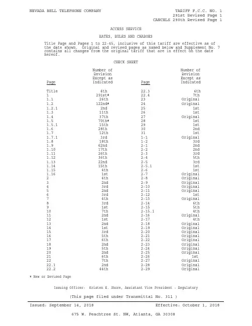
291st Revised Page 1CANCELS 290th Revised Page 1(This page filed under Transmittal No. 311 ) ACCESS SERVICERATES, RULES AND CHARGESTitle Page and Pages 1 to 22-45, inclusive of this tariff are effective as of the date shown. Original and revised pages as named below and Supplement No. 7 contains all changes from the original tariff that are in effect on the date hereof.CHECK SHEETNumber of Number of Revision Revision Except as Except asPageIndicated Page IndicatedTitle 4th 22.3 6th 1 291st*22.4 7th 1.1 26th 23O riginal 1.2 122nd* 24 O riginal 1.2.1 2nd 25 1st 1.3 11th 26 1st 1.4 37th 27O riginal 1.5 70th*28 1st 1.5.1 15th 29 1st 1.6 28th 30 2nd 1.7 12th 31 1st 1.7.1 3rd 1-1O riginal 1.8 18th 1-2 3rd 1.9 62nd 2-1 2nd 1.10 17th 2-2 2nd 1.11 26th 2-3 3rd 1.12 36th 2-4 5th 1.13 22nd 2-5 3rd 1.14 15th 2-5.1 1st 1.15 4th 2-6 1st 1.16 1st 2-7Original 2 4th 2-8Original 3 2nd 2-9Original 4 3rd 2-10Original 5 2nd 2-11Original 6 3rd 2-12 1st 7 4th 2-13Original 8 3rd 2-14 6th 9 1st 2-15 5th 10 7th 2-15.1 4th 11 2nd 2-16Original 12 1st 2-17 4th 13 2nd 2-18Original 14 1st 2-19Original 15 3rd 2-20Original 16 5th 2-21Original 17 6th 2-22Original 18 2nd 2-23Original 19 5th 2-24Original 20 2nd 2-25Original 21 6th 2-26 1st 22 7th 2-27Original 22.1 2nd 2-28Original 22.2 44th 2-29O riginal* New or Revised PageIssuing Officer: Kristen E. Shore, Assistant Vice President - RegulatoryRATES, RULES AND CHARGESCHECK SHEET (Cont’d)Number of Number ofRevision RevisionExcept as Except asPage Indicated Page Indicated3-13 2nd 5-11.2Original3-14 2nd 5-11.3Original3-15 2nd 5-12 1st3-16 1st 5-13 4th3-17 1st 5-14 4th3-18 1st 5-14.1Original3-19 Original 5-15 7th3-20 Original 5-16 3rd3-21 1st 5-17 11th3-22 1st 5-17.1 8th3-23 1st 5-17.1.1 6th3-24 2nd 5-17.2 7th3-25 1st 5-18 6th3-26 2nd 5-19 6th3-27 2nd 5-19.15th3-28 1st 5-19.2 4th3-29 2nd 5-19.3 4th3-30 1st 5-19.4 4th4-1 2nd 5-19.54th4-2 2nd 5-19.6 4th4-3 Original 5-19.74th4-4 4th 5-20 6th4-5 2nd 5-21Original4-6 1st 5-22Original4-7 1st 5-23Original4-8 2nd 5-24Original4th 5-25Original 4-8.14-9 67th*5-26 1st4-10 29th*5-27Original4-10.1 7th5-28Original4-11 72nd*6-1 3rd5-1 5th 6-2 1st5-2 2nd 6-31st5-3 7th 6-4 1st5-3.1 6th 6-5Original5-3.2 3rd 6-6Original5-3.3 3rd 6-7Original5-3.4 7th 6-8Original5-4 1st 6-9 1st5-5 1st 6-10 1st3rd 6-11Original 5-62nd 6-12Original 5-75-8 Original 6-13Original1st 6-14Original 5-93rd 6-15Original 5-105-11 2nd 6-16Original5-11.11st* New or Revised Page(This page filed under Transmittal No. 311 )ACCESS SERVICERATES, RULES AND CHARGESCHECK SHEET (Cont’d)Number of Revision Number of Revision Page Except as Indicated Page Except as Indicated7-26 Original 7-812nd 7-27 3rd 7-81.15th7-28 1st 7-81.24th7-29 Original 7-81.32nd 7-30 Original 7-81.49th 7-31 Original 7-81.56th7-32 Original 7-81.64th 7-33 3rd 7-81.6.1Original7-33.1 2nd 7-81.75th7-34 1st 7-81.8Original7-35 Original 7-8227th 7-36 Original 7-8311th 7-37 Original 7-8419th 7-38 Original 7-84.19th* 7-39 1st 7-852nd7-40 Original 7-85.11st 7-41 2nd 7-85.24th7-42 2nd 7-865th7-43 Original 7-875th 7-44 1st 7-87.15th7-45 Original 7-87.25th7-46 Original 7-87.34th 7-47 Original 7-87.44th 7-48 Original 7-882nd 7-49 2nd 7-892nd7-50 Original 7-903rd 7-51 Original 7-913rd 7-52 1st 7-91.15th7-53 1st 7-91.25th7-54 Original 7-91.2.12nd7-55 Original 7-91.32nd 7-56 10th 7-91.42nd7-57 Original 7-91.52nd 7-58 1st 7-91.62nd7-59 Original 7-91.72nd 7-60 Original 7-91.82nd 7-61 2nd 7-91.92nd7-62 3rd 7-91.102nd7-63 1st 7-926th7-64 3rd 7-935th7-65 1st 7-93.13rd7-66 5th 7-94Original7-66.1 2nd 8-13rd7-67 1st 8-24th7-68 Original 8-35th 7-69 3rd 8-3.13rd7-69.1 2nd 8-43rd7-69.2 2nd 8-53rd7-70 Original 8-62nd 7-71 Original 8-74th 7-72 Original 8-84th 7-73 10th 8-94th7-74 Original 8-104th 7-75 1st 8-114th7-76 Original 8-122nd 7-77 1st 8-132nd7-78 1st 8-142nd7-78.1 Original 8-155th 7-79 6th 8-163rd7-79.1 Original 8-175th 7-80 4th 8-184th8-193rd* New or Revised(This page filed under Transmittal No. 311 ) ACCESS SERVICE4. End User Access Service (Cont’d)4.6 Rate Regulations (Cont’d) 4.6.1 End User Common Line Rate Elements (Cont’d) (H) Federal Universal Service Fund (FUSF) Surcharge (Cont’d)(3) Other Non-recurring FUSF SurchargesIn addition to the applicable charges above, when a customer is assessed interstate end user chargesidentified in the table below, a FUSF Surcharge will also apply as set forth in Section 4.7(I) following. For example, customers assessed the PIC changecharge as specified in Section 13.3.3.(b)(5)(e)(ii) will also be assessed the PIC change FUSF Surcharge as set forth in Section 4.7(I) following.To the extent an IC is assessed a PIC Change Charge, the Non-recurring FUSF Surcharge will also apply to the IC.(4) Other FUSF SurchargesA percentage surcharge factor is assessed monthly on billed recurring and non-recurring charges of end user services other than surcharges described in Section 4.FUSF Surcharge factor: 0.201Tariff Reference Rate Element13.3.3(A)PIC Change Charge(I)(This page filed under Transmittal No. 311 ) ACCESS SERVICE4. End User Access Service (Cont’d)4.7 Rates and ChargesThe rates for End User Access are:(A) End User Common Line (EUCL) - Primary Residence SubscriberUSOC Rates Per Month - Individual lineor trunk, each 9ZEU1 $4.72(B) End User Common Line (EUCL) Non-Primary Residence Subscriber USOC Rates Per Month - Individual lineor trunk, each 9ZEU2 $4.72- BRI ISDN Facility, each wire pair 9ZEU5 4.72(C) End User Common Line (EUCL) -Single Line BusinessUSOC Rates Per Month - Individual lineor trunk, each 9ZEU3 $4.72(D) End User Common Line (EUCL) - Multiline Business SubscriberUSOC Rates Per Month - Individual lineor trunk, each 9ZEU4 $4.72- Public Telephone Access line, each 9ZEU4 4.72 - PRI ISDN Facility, each 9ZEU6 23.60(E) End User Common Line (EUCL) - Centrex CO and CO-like (Installedor on order prior to July 28, 1983)USOC Rates Per Month- Individual lineor trunk, each 9ZEU4 4.72(R) (R) (R) (R) (R) (R) (R) (R)ACCESS SERVICE4. End User Access Service (Cont’d)4.7 Rates and Charges (Cont’d)(G) Presubscribed Interexchange Carrier ChargesUSOC Rate Per Month(A) Multi-Line Business 9PCC4 0.00(B)ISDN-PRI-per service 9PCC6 0.00(C) Centrex CO andCentrexCO-Like-Nine or more lines, per line 9PCC7 0.00-Eight or less lines, per service 9PCC9 0.00(H) End User Port Charge USOC Rate Per Month(1) BRI ISDN Port- Per Port 9SDN1 $3.90(2) PRI ISDN Port- Per Port 9SDN2 $36.29(I)Basic FUSF Surcharge:USOC Rate Per Month(1) Residential 9PZRS $ 0.94(2) Single-Line Business 9PZBU $ 0.94(3) ISDN BRI 9PZL1 $ 1.73(4) Multiline Business 9PZLM $ 2.34(5) PRI ISDN 9PZP1 $18.99(6) PBX 9PZPX $ 2.34(7) Centrex CO and CO-Like 9PZCX $ 0.26(8) Other FUSF Surcharges USOC Rate Per Occurrence PIC Change Charge(a) Per Manual Change 9PZGM $ 0.78(b) Per Mechanized Change 9PZGE $ 0.32 (I) (I) (I) (I) (I) (I) (I) (I) (I)(This page filed under Transmittal No. 311 )(This page filed under Transmittal No. 311 ) ACCESS SERVICE7. Special Access Service (Cont'd)7.11 High Capacity Service 7.11.5 Rates and Charges General Description (Cont'd) 7.11.5.3 Rates and Charges (Cont'd)(F) DS1 Term Payment PlanRates and Charges for the DS1 Term Payment Plan (1)(1)Channel Termination - Per Point of TerminationUSOC1 Year2 Year3 Year 5 Year 7 Year TMECS $122.50 $120.00 $115.00 $104.00(R) $98.50(2) Channel Mileage- Channel Mileage Termination (per termination)- Channel Mileage Facility (per mile)USOC 1 Year 2 Year 3 Year 5 Year 7 Year 1L5XX$ 9.00$ 9.00$ 8.70$ 8.40$ 8.25(3) Central Office Multiplexing DS1 to DS0 voice/digital-Per arrangementUSOC1 Year2 Year3 Year 5 Year 7 Year MQ1, MQ1++,QMU, QMUA1, QMU++$180.00 $170.00 $170.00 $ 160.00 $150.00(4) Collocation Transport-Channel Mileage - FixedUSOC 1 Year 2 Year 3 Year 5 Year 7 Year 1H48S$ 51.00 $ 45.00 $ 40.00 $ 35.00 $ 32.50– Per Mile USOC 1 Year2 Year3 Year 5 Year 7 Year 1H48S$ 9.25$ 9.00$ 8.75$ 8.50$ 8.25(5) Nonrecurring Charges-One Time Charges- Per point of channel termination USOC DESCRIPTION RATE TMECS Channel Termination NonrecurringCharge$ 900.001H48S Collocation Transport NonrecurringChargeNOTE: Channel Termination Nonrecurring Charges and Collocation Transport Nonrecurring Chargesare waived on new installations of DS1 High Capacity Service with a 2, 3, 5, or 7 year DS1 TPP.(1) Effective on September 13, 2017, DS1 TPP 5- and 7-year Payment Plans are no longer available,including for any otherwise available conversions. Circuits already subject to a DS1 TPP 5- or 7-year Payment Plan, as of September 13, 2017, will continue to be provided under the then-current DS1 TPP 5- and 7-year Payment Plan term for the remainder of that term.USOC 1 Year 2 Year 3 Year 5 Year 7 Year 1L5XX$ 51.00$ 45.00$ 40.00$ 35.00$ 32.50。

胆⼤⼼细,2015款 27吋Retina 5K iMac MK472(中配)升级M.2 NVMe SSD + SATA 3 SSD·CZCZYX·⼀、目标2016年购入2015款 27吋Retina 5K iMac MK472(中配),原配256G SATA-e SSD,无机械硬盘,买了AC,未发生过故障。
购机后就自己增加过16G内存(共24G)。
平时喜欢折腾,经常感觉SSD容量太小,捉襟见肘。
很早就萌生了升级M.2 NVMe SSD的想法。
好不容易捱过了保修期,就做了些准备,开始动手了。
折腾的目标是把原配的SSD换成M.2 NVMe 1T SSD,一是增加了容量,二是体验NVMe 的高速。
另外,既然拆机了,就顺便在原机械硬盘位添加一块SATA3 1T SSD。
至于CPU就不升级了,感觉无此必要。
⼆、我准备的器材和⼯具1、970 Pro 1TB V-NAND 2bit MLC SSD一块2、1TB 3D Nand 2.5 Inch SATA III SSD一块3、适用于2012及更新款的27吋iMac HDD升级套件,包括:(1)HDD升级用串联数字温度热传感器电缆(不包括SATA III数据/电源电缆)(2)iMac屏幕拆卸专用滚轮(3)OEM屏幕胶条(4)屏幕玻璃吸盘2只(5)T8S、T10S螺丝起子各一把(6)撬棒(7)清洁布4、适用于2015年27吋A1419 iMac的 SATA III 硬盘数据/电源线一套5、M.2 NVMe SSD 2280转接卡一块(长卡),M2.5x8螺丝一只,M2.5垫片一片(说明:网购的转接卡一般只配M2x6螺丝一只,无法用于iMac)6、M.2 固态硬盘2280散热片(2~3mm厚纯紫铜质最好)及导热硅胶垫片、橡皮筋一套7、2.5吋转3.5吋硬盘金属托架一块,M3x5螺丝4只8、M3x8螺丝4只;直径约4.5mm的废圆珠笔芯塑料管,剪成每段约2mm长的4段(自制硬盘金属托架固定螺丝用)9、T5、T20螺丝起子各一把(我是用的以前网购的组合套件)10、直径2mm十字螺丝刀一支11、重要!一个macOS系统安装U盘。
HART ® Fieldbus ProfibusIntrinsic SafetyConfiguration Tools Semiconductors TrainingCustom DesignSmar ResearchTechnology SourceFeatures• Can be used in designs presently using the SYM20C15 or equivalent type chip• Single-chip, half-duplex 1200 bits per second FSK modem • Bell 202 shift frequencies of 1200 Hz and 2200 Hz • 3.3V-5.0V power supply• Transmit-signal wave shaping • Receive band-pass filter• Low power: optimal for intrinsically safe applications • CMOS compatible• Internal oscillator requires 460.8 kHz crystal or ceramic resonator • Meets HART physical layer requirements• Industrial temperature range of -40 °C to +85 °C• Available in a 28-pin PLCC and 32-pin LQFP packages(LQFP pictured)HART ModemHT2015 DataSheetThe HT2015 is a single-chip, CMOS modem for use in Highway Addressable Remote Transducer (HART) field instruments and masters. The modem and a few external passive components provide all of the functions needed to satisfy HART physical layer requirements including modulation, demodulation, receive filtering, carrier detect and transmit-signal shaping. The HT2015 is pin-compatible with theSYM20C15. See the Pin Description and Functional Description sections for details on pin compatibility with the SYM20C15.The HT2015 uses Phase Continuous Frequency Shift Keying (FSK) at 1200 bits per second. To conserve power the receive circuits are disabled during transmit operations and vice versa. This provides the half-duplex operation used in HART communications.General DescriptionFig. 1 - 28 pin PLCC Pinout Package Fig. 2 - 32 pin LQFP Pinout PackageTable 1 - Pin DescriptionsSignalTypePLCC LQFP DescriptionTEST1 Input 1 28 Connect to Vss.TEST2 * 2 29 No connect. TEST3 * 3 31 No connect. TEST4 * 4 32 No connect.TEST5 Input 5 1 Connect to Vss.INRESETInput62Reset all digital logic when low.TEST7 Input 7 3 Connect to Vss. TEST8Input84Connect to Vss.TEST9 Input 9 5 Connect to Vss. OTXAOutput107Modulated output transmit analog. FSK modulated HARTtransmit signal to 4-20mA loop interface circuit.IAREF Input 11 8 Analog reference voltage. ICDREFInput129Carrier detect reference voltage.OCBIAS Output 13 10 Comparator bias current. TEST10Input1411Connect to Vss.VDDA Power 15 13 Analog supply voltage. IRXA Input 16 14 FSK modulated HART receive signal from 4-20mA loopinterface circuit. .ORXAF Output 17 15 Analog receiver filter input. IRXACInput1816Analog receive comparator input.OXTL Output 19 17 Crystal oscillator output. IXTLInput2018Crystal oscillator input.VSS Ground 21 6,20 Ground. VDDPower2221,30Digital supply voltage.INRTS Input 23 22 Request to send. ITXDInput2423Input transmit data. Transmitted HART data stream fromUART.TEST11 * 25 24 No connect. ORXD Output 26 25 Received demodulated HART data to UART. OCD Output 27 26 Carrier detect output. TEST12*2827No connect.VSSA Ground * 12,19 Analog ground.Pin Descriptions:IAREF: Analog Reference VoltageThis analog input sets the dc operating point of the operational amplifiers and comparators and is usually selected to split the dc potential between V DD and V SS. See IAREF in DC Characteristics on page 11.ICDREF: Carrier Detect Reference VoltageThis analog input controls at which level the carrier detect (OCD) becomes active. This is determined by the dc voltage difference between ICDREF and IAREF. Selecting ICDREF - IAREF equal to 0.08 V DC will set the carrier detect to a nominal 100 mV p-p.INRESET: Reset Digital LogicWhen at logic low (V SS) this input holds all the digital logic in Reset. During normal operation INRESET should be at V DD. INRESET should be held low for a minimum of 10 nS after V DD = 2.5 V as shown in Figure 3.INRTS: Request To SendThis active-low input selects the operation of the modulator. OTXA is enabled when this signal is low. This signal must be held high during power-up.IRXA*: Analog Receive InputThis input accepts the 1200/2200 Hz signals from the external filter. IRXAC: Analog Receive Comparator InputThis is the positive input of the carrier detect comparator and the receiver filter comparator.ITXD: Digital Transmit Input (CMOS) This input to the modulator accepts digital data in NRZ form. When ITXD is low, the modulator output frequency is 2200 Hz. When ITXD is high, the modulator output frequency is 1200 Hz.IXTL: Oscillator InputThis input to the internal oscillator must be connected to a parallel mode 460.8 kHz ceramic resonator when using the internal oscillator or grounded when using an external 460.8 kHz clock signal. OCBIAS: Comparator Bias CurrentThe current through this output controls the operating parameters of the internal operational amplifiers and comparators. For normal operation, OCBIAS current is set to 2.5 4A.OCD: Carrier Detect OutputThis output goes high when a valid input is recognized on IRXA. If the received signal is greater than the threshold specified on ICDREF for four cycles of the IRXA signal,the valid input is recognized. Figure 3 - Reset TimingO RXAF*: Analog Receive Filter OutputThis signal is the square wave output of the receiver high-pass filter.ORXD: Digital Receive Output (CMOS) This signal outputs the digital receive data. When the received signal (IRXA) is 1200 Hz, ORXD outputs logic high. When the received signal (IRXA) is 2200 Hz, ORXD outputs logic low. ORXD is qualified internally with OCD and is logic high when OCD is low.OTXA: Analog Transmit OutputThis output provides the trapezoidal signal controlled by ITXD. When ITXD is low, the output frequency is 2200 Hz. When ITXD is high, the output frequency is 1200 Hz. This output is active when INRTS is low and 0.5 V DC when INRTS is high. OXTL: Oscillator OutputThis output from the internal oscillator must be connected to an external 460.8 kHz clock signal or to a parallel mode 460.8 kHz ceramic resonator when using the internal oscillator. TEST(12:1): Factory TestThese are factory test pins. For normal operation, tie these signals as per Table 1.VDD: Digital PowerThis is the power for the digital modem circuitry.VDDA: Analog Supply VoltageThis is the power for the analog modem circuitry.VSS: GroundThis is the analog and digital ground. VSSA: Analog GroundThe HT2015 is a functional equivalent of the SYM20C15 HART Modem. It contains a transmit data modulator and signal shaper, carrier detect circuitry, analog receiver and demodulator circuitry and an oscillator, as shown in Figure 4.The internal HART modem modulates the transmit-signal and demodulates the receive signal. The transmit-signal shaper enables theHT2015 to transmit a HART compliant signal. The carrier is detected by comparing the receiver filter output with the difference between two external voltage references. The analog receive circuitry band-pass filters the received signal for input to the modem and the carrier detect circuitry. The oscillator provides the modem with a stable time base using either a simple external resonator or an external clock source.Functional DescriptionFigure 4 - HT2015 Block DiagramHT2015 LOGIC The modem consists of a modulator and demodulator. The modem uses shift frequencies of nominally 1200 Hz (for a 1) and 2200 Hz (for a 0). The bit rate is1200 bits/second.Modulator The modulator accepts digital data in NRZ form at the ITXD input and generates the FSK modulated signal at the OTXA output. INRTS must be a logic low for the modulator to be active.Demodulator The demodulator accepts an FSK signal at the IRXA input and reproduces the original modulating signal at the ORXD output. Thenominal bit rate is 1200 bits per second. Figure 5 illustrates the demodulation process. The output of the demodulator is qualified with the carrier detect signal (OCD), therefore, only IRXA signals large enough to be detected (100 mVp-p typically) by the carrier detect circuit produce received serial data at ORXD. Maximum demodulator jitter is 12 percent of one bit given input frequencies within HARTspecifications, a clock frequency of 460.8 kHz (±1.0 percent) and zero input (IRXA) asymmetry.Modem CharacteristicsFigure 5: Demodulator Signal TimingTRANSMIT–SIGNAL SHAPER The transmit-signal shaper generates a HART compliant FSKmodulated signal at OTXA. Figure 6 and Figure 7 show the transmit-signal forms of the HT2015. For IAREF = 1.235 V DC , OTXA will have a voltage swing from approximately 0.25 to 0.75 V DC .CARRIER DETECT CIRCUITRY The Carrier Detect Comparator shown in Figure 8 below generates logic low output if the IRXAC voltage is belowICDREF. The comparator output is fed into a carrier detect block (see Figure 4 on page 5). The carrier detect block drives the carrier detect output pin OCD high if INRTS is high and four consecutive pulses out of thecomparator have arrived. OCD stays high as long as INRTS is high and the next comparator pulse is received in less than 2.5 ms. Once OCD goesinactive, it takes four consecutive pulses out of the comparator to assert OCD again. Four consecutive pulses amount to 3.33 ms when the received signal is 1200 Hz and to 1.82 ms when the received signal is 2200 HZ.Figure 7 - OTXA Waveform (2200 Hz)Figure 6 - OTXA Waveform (1200 Hz)ANALOG RECEIVER CIRCUITRYVoltage References The HT2015 requires two voltage references, IAREF and ICDREF. IAREF sets the dc operating point of the internal operational amplifiers and comparators. A 1.235 V DC reference (Analog Devices AD589) is suitable as IAREF. The level at which OCD (carrier detect) becomes active is determined by the dc voltage difference (ICDREF - IAREF). Selecting a voltage difference of 0.08 V DC will set the carrier detect to a nominal 100 mV p-p .Bias Current Resistor The HT2015 requires a bias current resistor to beconnected between OCBIAS and V SS . The bias current controls the operating parameters of the internal operational amplifiers and comparators. The value of the bias current resistor is determined by the referencevoltage IAREF and the following formula:The recommended bias current resistor is 500 ohm; when IAREF is equal to 1.235 V DC . In Figure 8 all external capacitor values have a tolerance of ±5 percent and the resistors have a tolerance of ±1 percent, except the 3 ohm; which has a tolerance of ±5 percent. External to the HT2015, the filter exhibits a three-pole, high-pass filter at 624 Hz and a one-pole, low-pass filter at 2500 Hz.Internally, the HT2015 has a high-pass pole at 35 Hz and a low-pass pole at 90 kHz. The low-pass pole can vary as much as ±30 percent. The inputimpedance of the entire filter is greater than 150 ohm; at frequencies below 50 kHz.Figure 8 - Receive Filter SchematicR BIAS =OSCILLATOR The HT2015 requires a 460.8 kHz clock signal on OXTL. This can be provided by an external clock or external components may be connected to the HT2015 internal oscillator.Internal Oscillator Option The oscillator cell will function with either a 460.8 kHz crystal orceramic resonator. A parallel resonant ceramic resonator can be connected between OXTL and IXTL. Figure 9 illustrates the crystal option for clock generation using a 460.8 kHz (±I percent tolerance) parallel resonant crystal and two tuning capacitors. The actual values of the capacitors maydepend on the recommendations of the manufacturer of the resonator. Typically, capacitors in the range of 100 pF to 470 pF are used.External Clock Option It may be desirable to use an external 460.8 kHz clock as shown in Figure 10 rather than the internaloscillator because of the high cost and low availability of ceramic resonators. In addition, the HT2015 consumes less current when an external clock is used. Minimum current consumption occurs with the clock connected to OXTL and IXTL connected to V SS .Figure 10 -Oscillator with External ClockFigure 9 - Crystal OscillatorElectrical CharacteristicsT A Ambient -40 CABSOLUTE MAXIMUMS+85 T S Storage Temperature -55 150 CV DD Supply Voltage - .3 6.0 VV IN , V OUT DC Input, Output - .3 V DD + .3 VT L Lead Temperature (soldering) 250 CCautions:1. CMOS devices are damaged by high-energy electrostatic discharge. Devices must be stored in conductivefoam or with all pins shunted. Precautions should be taken to avoid application of voltages higher than themaximum rating. Stresses above absolute maximum ratings may result in damage to the device.2. Remove power before insertion or removal of this device. V IL Input Voltage, Low VDC CHARACTERISTICS(V DD = 3.0V to 5.5V, V SS = 0V, T A = -40C to +85C).3 * V DD V IH Input Voltage .7 * V DD VV OL Output Voltage, Low (IOL = .67mA) .4 VV OH Output Voltage, High (IOH = .67mA) 2.4 VC IN Input Capacitance Analog Input IRXA Digital InputpF3.0 - 5.5 3.0 - 5.5 3.0 - 5.5 3.0 - 5.5 2.9 253.5I IL/IH Input Leakage Current +/-500 nAI OLL Output Leakage Current +/-10 µAI DD Power Supply Current (RBIAS = 500k Ω, IAREF = 1.235V) 3.3 5.0 150 170 180 200µAIAREF Analog Reference 3.3 5.0 1.2 1.235 2.52.6 VICDREF * Carrier Detect Reference (IAREF = .08V)1.15 VOCBIAS Comparator Bias Current (RBIAS = 500k Ω, IAREF = 1.235V)2.5 µA* The HART specification requires Carrier Detect (OCD) to be active between 80 and 120 mV p-p.Setting ICDREF at IAREF—.08V DC will set the carrier detect to a nominal 100 mV p-p.Demodulator JitterConditions1. Input frequencies at 1200 Hz +/-10 Hz, 2200 Hz +/-20 Hz2. Clock frequency of 460.8 kHz +/-0.1%3. Input (HLXA) asymmetry, 0 % of 1 bitMODEM CHARACTERISTIC(V DD = 3.0V to 5.5V, V SS = OV, T A = -40 C to +85 C)12 ResonatorToleranceFrequency 460.8% kHzCERAMIC RESONATOR - EXTERNAL CLOCK SPECIFICATIONS(V DD = 3.0V to 5.5V, V SS = OV, T A = -40 C to +85 C)1.0ExternalClock Frequency Duty Cycle Amplitude456.240460.850V OH - V OL465.460kHz%V AC CHARACTERISTICS(V DD = 3.0V to 5.5V, V SS = 0V, T A = -40C to +85C)IRXA Receive Analog InputLeakage CurrentFrequency - Mark (Logic 1) Frequency - Space (Logic 0) 1190218012002200+/-15012102220nAHzHzORXAF Output of the High-pass FilterSlew RateGain Bandwidth (GBW) Voltage Range 150.15.025V DD - .15V/µskHzV/µsIRXAC Carrier Detect & Receive Filter InputLeakage Current+/-500 nA OTXA ModulatorOutputFrequency * - Mark (Logic 1)Frequency - Space (Logic 0)Amplitude (IAREF 1.235 V)SlopeLoading (IAREF = 1.235 V) 30 1196.92194.35002.79HzHzmV p-pmV/µskΩORXD ReceiveDigitalOutputRise/Fall Time 20nsOCD Carrier Detect OutputRise/Fall Time 20ns * The modular output frequencies are proportional to the input clock frequency (460.8 kHz)Mechanical SpecificationFigure 11 - 28-pin PLCC Mechanical SpecificationA .165 .172 .180A 1 .099 .101 .110D .485 .490 .495D 1 .450 .452 .455D 2 .390 .420 .430D 3E .485 .490 .495E 1 .450 .452 .455E 2 .390 .420 .430E 3 .300 REFe .050 BSC.300 REFFigure 12 - 32-pin LQFP Mechanical SpecificationA - - 1.60A 1 .05 .01 .15A 2 1.35 1.40 1.45D 9.00 BSCD /2 4.50 BSCD 1 7.00 BSCE 9.00 BSCE /2 4.50 BSCE 1 L .45 .60 .75e .80 BSCb .30 .37 .45c .09 - .20ccc - - .10ddd - - .207.00 BSCSmar Research Corporation4250 Veterans Memorial HighwayHolbrook, NY USA 11741Tel: 631.737.3111 Fax: 631.737.3892techinfo@Smar Research reserves the right to make changes to design and functionality of any product without notice. Smar Research does not assumeany liability arising out of the application or use of any product. Smar Research , Technology Source, and the SRC logo are registered trademarks of Smar Research Corporation. The HART, Fieldbus, and Profibus Foundation logos are trademarks of their respective owners.。

稀土元素是镧系元素系稀土类元素群的总称,包含钪Sc、钇Y及镧系中的镧La、铈Ce、镨Pr、钕Nd、钷Pm、钐Sm、铕Eu、钆Gd、铽Tb、镝Dy、钬Ho、铒Er、铥Tm、镱Yb、镥Lu,共17个元素。
镧(lan兰)、铈(shi市)、镨(pu普)、钕(nv女)、钷(po叵)、钐(shan山)、铕(you 有)、钆(ga嘎)、铽(te特)、镝(di笛)、钬(huo火)、铒(er耳)、铥(diu丢)、镱(yi 意)、镥(lu鲁),钪(kang抗),钇(yi乙)“稀土”一词是十八世纪沿用下来的名称,因为当时用于提取这类元素的矿物比较稀少,而且获得的氧化物难以熔化,也难以溶于水,也很难分离,其外观酷似“土壤”,而称之为稀土。
稀土元素分为“轻稀土元素”和“重稀土元素”:“轻稀土元素”指原子序数较小的钪Sc、钇Y和镧La、铈Ce、镨Pr、钕Nd、钷Pm、钐Sm、铕Eu。
“重稀土元素”原子序数比较大的钆Gd、铽Tb、镝Dy、钬Ho、铒Er、铥Tm、镱Yb、镥Lu。
二、稀土资源及储备状况由于稀土元素性质活跃,使它成为亲石元素,地壳中还没有发现它的天然金属无水或硫化物,最常见的是以复杂氧化物、含水或无水硅酸盐、含水或无水磷酸盐、磷硅酸盐、氟碳酸盐以及氟化物等形式存在。
由于稀土元素的离子半径、氧化态和所有其它元素都近似,因此在矿物中它们常与其它元素一起共生。
我国稀土资源占世界稀土资源的80%,以氧化物(REO)计达3 600万吨,远景储量实际是1亿吨。
我国稀土资源分南北两大块。
——北方:轻稀土资源,集中在包头白云鄂博特等地,以后在四川冕宁又有发现。
主要含镧、铈、镨、钕和少量钐、铕、钆等元素;——南方:中重稀土资源,分布在江西、广东、广西、福建、湖南等省,以罕见的离子态赋存与花岗岩风化壳层中,主要含钐、铕、钆、铽、镝、钬、铒、铥、镱、镥、钇和镧、钕等元素。
DXi 系列磁盘备份解决方案利用 Quantum 的重复数据删除技术,将磁盘需求量降低了 90% 甚至更高,同时支持通过WAN 在各地之间复制数据,实现了灾难恢复保护。
DXi 系列设备提供业界最大的备份容量范围,原始磁盘的容量从1.2TB 到 240TB 不等。
各型号的设备通过统一技术、复制功能和管理层相连,使得 IT 部门能够通过一项全面的数据保护策略联系各个分支机构,这项策略可显著提高备份性The DXi-Series disk backup solutions leverage data de-duplication technology to reduce disk requirements by 90% or more and make WAN-based replication a practical DR tool. The DXi-Series spans the widest range of backup capacity points in the industry, from 1.2TB to 240TB of raw disk capacity. All models are connected by a common technology base, replication capability, and management layer. This allows IT departments to connect all their sites in a comprehensive data protection strategy that boosts backup performance, and reduces or eliminates media handling, all without备份性能DXi 系列磁盘备份与复制系统利用 Quantum 已获专利的重复数据删除技术,大大提高了磁盘在关键数据保护中所能发挥的作用。
本次调查应在您家登记的人包括:
• 2015年10月31日晚住在您家里的人,但不包括由于临时出差、探亲或旅游等 2015年10月31日晚暂住在您家的人。
• 户口登记在您家现住房地址的人。
• 经常居住在您家,由于临时出差、探亲、旅游或值夜班等2015年10月31日晚 未住在您家的人。
• 幼儿园全托孩子、小学和初中住校生。
不包括:
• 现役军人和武警。
• 港澳台居民和外国人。
• 2015年11月1日零时以后出生的人。
您家填报调查表的人数为 人
表 号:制定机关:文 号:有效期至:R 5 0 1表国家统计局国统字(2015) 50号2 0 1 5年1 2月
申报人(签字):调查员(签字):
填报日期:2015年11月 日
地址:
县(市、区) 乡(镇、街道) 村(居)委会 调查小区 户编号
20152015年全国1%人口抽样调查表(备用表)。