ATMEL 单片机选型指南
- 格式:pdf
- 大小:732.63 KB
- 文档页数:21
专利证书网站首页由单片机实现检测控制,其中一个首要的工作就是选择合适的单片机。
目前国内在使用单片机作控制系统的微处理器时多选择51系列或Motorola 系列单片机,而本系统选用的PIC系列单片机在多个方面较其它系列单片机更有优越性。
下面对PIC单片机作较详细介绍。
2.4.l由单片机实现检测控制,其中一个首要的工作就是选择合适的单片机。
目前国内在使用单片机作控制系统的微处理器时多选择51系列或Motorola当今世界上涌现出各种各样的单片机,目前应用较广的主要有美国Intel公司开发和生产的MCS一51,MCS一96系列、台湾ICSI公司的8051系列、美国Motorola公司的MC68系列和美国Microchip公司的PIC系列等,其中各个系列的单片机都有其各自的优点,与其它系列相比,美国力,从而提高了工业电脑自动控制器的适应能力,以下分几个方面通过与其它类型单片机的比较来说明它的优越之处。
(l)哈佛总线结构 PIC系列单片机在架构上采用了与众不同的设计手法,PIC系列单片机不仅采用了哈佛体系结构(也就是两种存储器位于不同的逻辑空间里,这种架构的微控制器、微处理器、数字信号处理器或者微型计算机系统,称为哈佛体系结构),而且还采用了哈佛总线结构。
在PIC系列单片机中采用的这种哈佛总线结构,就是在芯片内部将数据总线和指令总线分离,并且采用不同的宽度,这样做的好处是,便于实现指令提取的“流水作业”,也就是在执行一条指令的同时对下一条指令进行取指令操作;便于实现全部指令的单字节化、单周期化,从而有利于提高CP U执行指令的速度。
在一般的单片机中,指令总线和数据总线是共用的(即分时复用)Motorola公司开发的MC68H C05/08系列单片机,其程序存储器和数据存储器统一编址(也就是两种存储器位于同一个逻辑空间里,这种架构的微控制器、微处理器、数字信号处理器或者微型计算机系统,称为普林斯顿体系结构),早期在国内市场上最流行的单片机产品Intel开发生产的MCS一51系列单片机,其程序存储器和数据存储器虽然独立编址;但是它们与CP U之间传递信息必须共用同一条总线,仍然摆脱不了瓶颈效应的制约,于是影响到CP U运行速度的进一步提高。
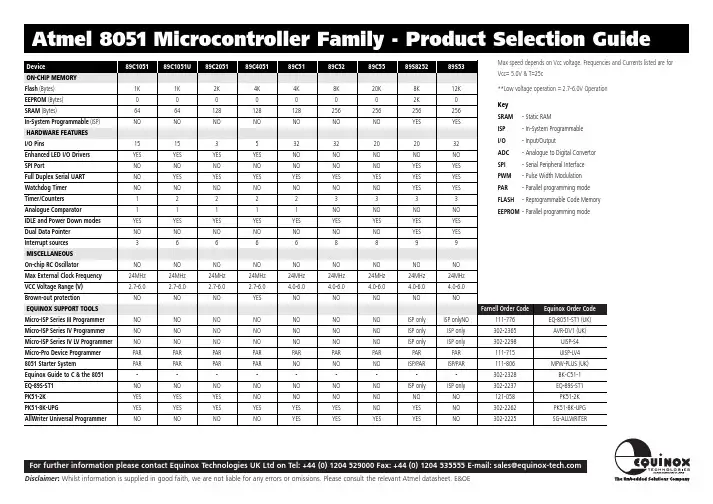
Continued....Features Array•Compatible with MCS-51™ Products•4K Bytes of Reprogrammable Flash Memory–Endurance: 1,000 Write/Erase Cycles• 3.0V to 6V Operating Range•Fully Static Operation: 0 Hz to 24 MHz•Two-Level Program Memory Lock•128 x 8-Bit Internal RAM•15 Programmable I/O Lines•Two 16-Bit Timer/Counters•Six Interrupt Sources•Programmable Serial UART Channel•Direct LED Drive Outputs•On-Chip Analog Comparator•Low Power Idle and Power Down Modes•Brown-Out DetectionDescriptionThe AT89C4051 is a low-voltage, high-performance CMOS 8-bit microcomputer with 4K Bytes of Flash programmable and erasable read only memory (PEROM). The device is manufactured using Atmel’s high density nonvolatile memory technology and is compatible with the industry standard MCS-51™ instruction set. By combining a versatile 8-bit CPU with Flash on a monolithic chip, the Atmel AT89C4051 is a pow-erful microcomputer which provides a highly flexible and cost effective solution to many embedded control applications.The AT89C4051 provides the following standard features: 4K Bytes of Flash, 128 bytes of RAM, 15 I/O lines, two 16-bit timer/counters, a five vector two-level interrupt architecture, a full duplex serial port, a precision analog comparator, on-chip oscillator and clock circuitry. In addition, the AT89C4051 is designed with static logic for opera-tion down to zero frequency and supports two software-selectable power saving modes. The Idle Mode stops the CPU while allowing the RAM, timer/counters, serial port and interrupt system to continue functioning. The Power Down Mode saves the RAM contents but freezes the oscillator disabling all other chip functions until the nexthardware reset.Block DiagramAT89C4051Pin DescriptionV CCSupply voltage.GNDGround.Port 1Port 1 is an 8-bit bidirectional I/O port. Port pins P1.2 to P1.7 provide internal pullups. P1.0 and P1.1 require exter-nal pullups. P1.0 and P1.1 also serve as the positive input (AIN0) and the negative input (AIN1), respectively, of the on-chip precision analog comparator. The Port 1 output buffers can sink 20 mA and can drive LED displays directly. When 1s are written to Port 1 pins, they can be used as inputs. When pins P1.2 to P1.7 are used as inputs and are externally pulled low, they will source current (I IL) because of the internal pullups.Port 1 also receives code data during Flash programming and verification.Port 3Port 3 pins P3.0 to P3.5, P3.7 are seven bidirectional I/O pins with internal pullups. P3.6 is hard-wired as an input to the output of the on-chip comparator and is not accessible as a general purpose I/O pin. The Port 3 output buffers can sink 20 mA. When 1s are written to Port 3 pins they are pulled high by the internal pullups and can be used as inputs. As inputs, Port 3 pins that are externally being pulled low will source current (I IL) because of the pullups. Port 3 also serves the functions of various special features of the AT89C4051 as listed below:Port 3 also receives some control signals for Flash pro-gramming and verification.RSTReset input. All I/O pins are reset to 1s as soon as RST goes high. Holding the RST pin high for two machine cycles while the oscillator is running resets the device.Each machine cycle takes 12 oscillator or clock cycles. XTAL1Input to the inverting oscillator amplifier and input to the internal clock operating circuit. XTAL2Output from the inverting oscillator amplifier.Oscillator CharacteristicsXTAL1 and XTAL2 are the input and output, respectively, of an inverting amplifier which can be configured for use as an on-chip oscillator, as shown in Figure 1. Either a quartz crystal or ceramic resonator may be used. To drive the device from an external clock source, XTAL2 should be left unconnected while XTAL1 is driven as shown in Figure 2. There are no requirements on the duty cycle of the external clock signal, since the input to the internal clocking circuitry is through a divide-by-two flip-flop, but minimum and maxi-mum voltage high and low time specifications must be observed.Figure 1. Oscillator ConnectionsNote:C1, C2= 30 pF ± 10 pF for Crystals= 40 pF ± 10 pF for Ceramic Resonators Figure 2. External Clock Drive ConfigurationPort Pin Alternate FunctionsP3.0RXD (serial input port)P3.1TXD (serial output port) P3.2INT0 (external interrupt 0) P3.3INT1 (external interrupt 1) P3.4T0 (timer 0 external input) P3.5T1 (timer 1 external input)Special Function RegistersA map of the on-chip memory area called the Special Func-tion Register (SFR) space is shown in the table below. Note that not all of the addresses are occupied, and unoc-cupied addresses may not be implemented on the chip. Read accesses to these addresses will in general return random data, and write accesses will have an indetermi-nate er software should not write 1s to these unlisted loca-tions, since they may be used in future products to invoke new features. In that case, the reset or inactive values of the new bits will always be 0.Table 1. AT89C4051 SFR Map and Reset Values0F8H0FFH0F0H B000000000F7H 0E8H0EFH0E0H ACC000000000E7H 0D8H0DFH0D0H PSW000000000D7H 0C8H0CFH 0C0H0C7H0B8H IPXXX000000BFH0B0H P3111111110B7H0A8H IE0XX000000AFH 0A0H0A7H98H SCON00000000SBUFXXXXXXXX9FH90H P11111111197H88H TCON00000000TMOD00000000TL000000000TL100000000TH000000000TH1000000008FH80H SP00000111DPL00000000DPH00000000PCON0XXX000087HAT89C4051Restrictions on Certain InstructionsThe AT89C4051 is an economical and cost-effective mem-ber of Atmel’s growing family of microcontrollers. It contains 4K bytes of flash program memory. It is fully compatible with the MCS-51 architecture, and can be programmed using the MCS-51 instruction set. However, there are a few considerations one must keep in mind when utilizing certain instructions to program this device.All the instructions related to jumping or branching should be restricted such that the destination address falls within the physical program memory space of the device, which is 4K for the AT89C4051. This should be the responsibility of the software programmer. For example, LJMP 0FE0H would be a valid instruction for the AT89C4051 (with 4K of memory), whereas LJMP 1000H would not.1. Branching instructions:LCALL, LJMP, ACALL, AJMP, SJMP, JMP @A+DPTR These unconditional branching instructions will execute correctly as long as the programmer keeps in mind that the destination branching address must fall within the physical boundaries of the program memory size (locations 00H to FFFH for the 89C4051). Violating the physical space limits may cause unknown program behavior.CJNE [...], DJNZ [...], JB, JNB, JC, JNC, JBC, JZ, JNZ With these conditional branching instructions the same rule above applies. Again, violating the memory boundaries may cause erratic execution.For applications involving interrupts the normal interrupt service routine address locations of the 80C51 family archi-tecture have been preserved.2. MOVX-related instructions, Data Memory:The AT89C4051 contains 128 bytes of internal data mem-ory. Thus, in the AT89C4051 the stack depth is limited to 128 bytes, the amount of available RAM. External DATA memory access is not supported in this device, nor is exter-nal PROGRAM memory execution. Therefore, no MOVX [...] instructions should be included in the program.A typical 80C51 assembler will still assemble instructions, even if they are written in violation of the restrictions men-tioned above. It is the responsibility of the controller user to know the physical features and limitations of the device being used and adjust the instructions used correspond-ingly.Program Memory Lock BitsOn the chip are two lock bits which can be left unpro-grammed (U) or can be programmed (P) to obtain the addi-tional features listed in the table below:Lock Bit Protection Modes(1)Note: 1.The Lock Bits can only be erased with the Chip Erase operation.Idle ModeIn idle mode, the CPU puts itself to sleep while all the on-chip peripherals remain active. The mode is invoked by software. The content of the on-chip RAM and all the spe-cial functions registers remain unchanged during this mode. The idle mode can be terminated by any enabled interrupt or by a hardware reset.P1.0 and P1.1 should be set to ’0’ if no external pullups are used, or set to ’1’ if external pullups are used.It should be noted that when idle is terminated by a hard-ware reset, the device normally resumes program execu-tion, from where it left off, up to two machine cycles before the internal reset algorithm takes control. On-chip hardware inhibits access to internal RAM in this event, but access to the port pins is not inhibited. To eliminate the possibility of an unexpected write to a port pin when Idle is terminated by reset, the instruction following the one that invokes Idle should not be one that writes to a port pin or to external memory.Power Down ModeIn the power down mode the oscillator is stopped, and the instruction that invokes power down is the last instruction executed. The on-chip RAM and Special Function Regis-ters retain their values until the power down mode is termi-nated. The only exit from power down is a hardware reset. Reset redefines the SFRs but does not change the on-chip RAM. The reset should not be activated before V CC is restored to its normal operating level and must be held active long enough to allow the oscillator to restart and sta-bilize.P1.0 and P1.1 should be set to ’0’ if no external pullups are used, or set to ’1’ if external pullups are used.Program Lock BitsLB1LB2Protection Type1U U No program lock features.2P U Further programming of the Flashis disabled.3P P Same as mode 2, also verify isdisabled.Brown-Out DetectionWhen V CC drops below the detection threshold, all port pins (except P1.0 and P1.1) are weakly pulled high. When V CC goes back up again, an internal Reset is automatically generated after a delay of typically 15 msec. The nominal brown-out detection threshold is 2.3V ± 10%.Programming The FlashThe AT89C4051 is shipped with the 4K bytes of on-chip PEROM code memory array in the erased state (i.e., con-tents = FFH) and ready to be programmed. The code mem-ory array is programmed one byte at a time. Once the array is programmed, to re-program any non-blank byte, the entire memory array needs to be erased electrically. Internal Address Counter: The AT89C4051 contains an internal PEROM address counter which is always reset to 000H on the rising edge of RST and is advanced by apply-ing a positive going pulse to pin XTAL1.Programming Algorithm: To program the AT89C4051, the following sequence is recommended.1.Power-up sequence:Apply power between V CC and GND pinsSet RST and XTAL1 to GND2.Set pin RST to ’H’Set pin P3.2 to ’H’3.Apply the appropriate combination of ’H’ or ’L’ logiclevels to pins P3.3, P3.4, P3.5, P3.7 to select one of the programming operations shown in the PEROM Pro-gramming Modes table.To Program and Verify the Array:4.Apply data for Code byte at location 000H to P1.0 toP1.7.5.Raise RST to 12V to enable programming.6.Pulse P3.2 once to program a byte in the PEROM arrayor the lock bits. The byte-write cycle is self-timed and typically takes 1.2 ms.7.To verify the programmed data, lower RST from 12V tologic ’H’ level and set pins P3.3 to P3.7 to the appropriate levels. Output data can be read at the port P1 pins.8.To program a byte at the next address location, pulseXTAL1 pin once to advance the internal address counter.Apply new data to the port P1 pins.9.Repeat steps 5 through 8, changing data and advancingthe address counter for the entire 4K bytes array or until the end of the object file is reached.10.Power-off sequence:set XTAL1 to ’L’set RST to ’L’Turn V CC power offData Polling: The AT89C4051 features Data Polling to indicate the end of a write cycle. During a write cycle, an attempted read of the last byte written will result in the com-plement of the written data on P1.7. Once the write cycle has been completed, true data is valid on all outputs, and the next cycle may begin. Data Polling may begin any time after a write cycle has been initiated.Ready/Busy: The Progress of byte programming can also be monitored by the RDY/BSY output signal. Pin P3.1 is pulled low after P3.2 goes High during programming to indi-cate BUSY. P3.1 is pulled High again when programming is done to indicate READY.Program Verify: If lock bits LB1 and LB2 have not been programmed code data can be read back via the data lines for verification:1.Reset the internal address counter to 000H by bringingRST from ’L’ to ’H’.2.Apply the appropriate control signals for Read Code dataand read the output data at the port P1 pins.3.Pulse pin XTAL1 once to advance the internal addresscounter.4.Read the next code data byte at the port P1 pins.5.Repeat steps 3 and 4 until the entire array is read.The lock bits cannot be verified directly. Verification of the lock bits is achieved by observing that their features are enabled.Chip Erase: The entire PEROM array (4K bytes) and the two Lock Bits are erased electrically by using the proper combination of control signals and by holding P3.2 low for 10 ms. The code array is written with all “1”s in the Chip Erase operation and must be executed before any non-blank memory byte can be re-programmed.AT89C4051Reading the Signature Bytes: The signature bytes are read by the same procedure as a normal verification of locations 000H, 001H, and 002H, except that P3.5 and P3.7 must be pulled to a logic low. The values returned are as follows.(000H) = 1EH indicates manufactured by Atmel (001H) = 41H indicates 89C4051Programming InterfaceEvery code byte in the Flash array can be written and the entire array can be erased by using the appropriate combi-nation of control signals. The write operation cycle is self-timed and once initiated, will automatically time itself to completion.All major programming vendors offer worldwide support for the Atmel microcontroller series. Please contact your local programming vendor for the appropriate software revision.Flash Programming ModesNotes:1.The internal PEROM address counter is reset to 000H on the rising edge of RST and is advanced by a positive pulse atXT AL 1 pin.2.Chip Erase requires a 10-ms PROG pulse.3.P3.1 is pulled Low during programming to indicate RDY/BSY .ModeRST/VPP P3.2/PROGP3.3P3.4P3.5P3.7Write Code Data (1)(3)12VLHHHRead Code Data (1)H H L L H H Write LockBit - 112VHHHHBit - 212V H H L LChip Erase 12VH L L LRead Signature Byte H H L L L L(2)Figure 3. Programming the Flash MemoryFigure 4. Verifying the Flash MemoryFlash Programming and Verification CharacteristicsT A = 0°C to 70°C, V CC = 5.0 ± 10%Note:1. Only used in 12-volt programming mode.Symbol ParameterMin Max Units V PP Programming Enable Voltage 11.512.5V I PP Programming Enable Current 250µA t DVGL Data Setup to PROG Low 1.0µs t GHDX Data Hold After PROG 1.0µs t EHSH P3.4 (ENABLE) High to V PP 1.0µs t SHGL V PP Setup to PROG Low 10µs t GHSL V PP Hold After PROG 10µs t GLGH PROG Width1110µs t ELQV ENABLE Low to Data Valid 1.0µs t EHQZ Data Float After ENABLE 0 1.0µs t GHBL PROG High to BUSY Low 50ns t WC Byte Write Cycle Time2.0ms t BHIH RDY/BSY\ to Increment Clock Delay1.0µs t IHIL Increment Clock High200nsAT89C4051Flash Programming and Verification WaveformsAbsolute Maximum Ratings*Operating Temperature.................................-55°C to +125°C *NOTICE:Stresses beyond those listed under “Absolute Maximum Ratings” may cause permanent dam-age to the device. This is a stress rating only and functional operation of the device at these or any other conditions beyond those indicated in the operational sections of this specification is not implied. Exposure to absolute maximum rating conditions for extended periods may affect device reliability.Storage T emperature.....................................-65°C to +150°C Voltage on Any Pinwith Respect to Ground.....................................-1.0V to +7.0V Maximum Operating Voltage.............................................6.6V DC Output Current......................................................25.0 mADC CharacteristicsT A = -40°C to 85°C, V CC = 3.0V to 6.0V (unless otherwise noted)Notes:1.Under steady state (non-transient) conditions, I OL must be externally limited as follows:Maximum I OL per port pin: 20 mAMaximum total I OL for all output pins: 80 mAIf I OL exceeds the test condition, V OL may exceed the related specification. Pins are not guaranteed to sink current greater than the listed test conditions.2.Minimum V CC for Power Down is 2V .Symbol Parameter ConditionMin Max Units V IL Input Low Voltage -0.50.2 V CC - 0.1V V IH Input High Voltage (Except XT AL1, RST)0.2 V CC + 0.9V CC + 0.5V V IH1Input High Voltage (XT AL1, RST)0.7 V CCV CC + 0.5V V OL Output Low Voltage (1)(Ports 1, 3)I OL = 20 mA, V CC = 5V I OL = 10 mA, V CC = 2.7V 0.5V V OHOutput High Voltage (Ports 1, 3)I OH = -80 µA, V CC = 5V ± 10% 2.4V I OH = -30 µA 0.75 V CCV I OH = -12 µA0.9 V CCVI IL Logical 0 Input Current (Ports 1, 3)V IN = 0.45V-50µA I TL Logical 1 to 0 T ransition Current (Ports 1, 3)V IN = 2V , V CC = 5V ± 10%-750µA I LI Input Leakage Current (Port P1.0, P1.1)0 < V IN < V CC ±10µA V OS Comparator Input Offset Voltage V CC = 5V20mV V CM Comparator Input Common Mode Voltage0V CC V RRST Reset Pulldown Resistor 50300K ΩC IO Pin Capacitance T est Freq. = 1 MHz, T A = 25°C 10pF I CCPower Supply CurrentActive Mode, 12 MHz, V CC = 6V/3V 15/5.5mA Idle Mode, 12 MHz, V CC = 6V/3V P1.0 & P1.1 = 0V or V CC5/1mA Power Down Mode (2)V CC = 6V P1.0 & P1.1 = 0V or V CC 100µA V CC = 3V P1.0 & P1.1 = 0V or V CC20µAExternal Clock Drive WaveformsExternal Clock DriveSymbol Parameter V CC = 3.0V to 6.0V V CC = 4.0V to 6.0V UnitsMin Max Min Max1/t CLCL Oscillator Frequency012024MHz t CLCL Clock Period83.341.6ns t CHCX High Time3015ns t CLCX Low Time3015ns t CLCH Rise Time2020ns t CHCL Fall Time2020nsSerial Port Timing: Shift Register Mode Test Conditions(V CC = 5.0V ± 20%; Load Capacitance = 80 pF)Shift Register Mode Timing WaveformsSymbolParameter12 MHz Osc Variable Oscillator UnitsMinMaxMin Maxt XLXL Serial Port Clock Cycle Time1.012t CLCL µs t QVXH Output Data Setup to Clock Rising Edge 70010t CLCL -133ns t XHQX Output Data Hold After Clock Rising Edge 502t CLCL -117ns t XHDX Input Data Hold After Clock Rising Edge 0ns t XHDVClock Rising Edge to Input Data Valid70010t CLCL -133nsAC Testing Input/Output Waveforms (1)Note: 1.AC Inputs during testing are driven at V CC - 0.5V for a logic 1 and 0.45V for a logic 0. Timing measure-ments are made at V IH min. for a logic 1 and V IL max. for a logic 0.Float Waveforms (1)Note: 1.For timing purposes, a port pin is no longer float-ing when a 100 mV change from load voltage occurs. A port pin begins to float when 100 mV change frothe loaded V OH /V OLlevel occurs.Notes: 1.XT AL1 tied to GND for I CC (power down)2.P.1.0 and P1.1 = V CC or GND3.Lock bits programmedOrdering InformationSpeed (MHz)PowerSupply Ordering Code Package Operation Range12 3.0V to 6.0V A T89C4051-12PCA T89C4051-12SC 20P320SCommercial(0°C to 70°C)A T89C4051-12PI A T89C4051-12SI 20P320SIndustrial(-40°C to 85°C)A T89C4051-12P A A T89C4051-12SA 20P320SAutomotive(-40°C to 105°C)24 4.0V to 6.0V A T89C4051-24PCA T89C4051-24SC 20P320SCommercial(0°C to 70°C)A T89C4051-24PI A T89C4051-24SI20P320SIndustrial(-40°C to 85°C) Package Type20P320 Lead, 0.300” Wide, Plastic Dual In-line Package (PDIP)20S20 Lead, 0.300” Wide, Plastic Gull Wing Small Outline (SOIC)AT89C4051 Packaging Information。
单片机选型注意事项
在单片机应用系统开发中,单片机是整个设计的核心,设计者需要为单片机侵扰合适的外部器件,同时还需要设计整个控制软件,因此选择合适的单片机型号很重要。
目前,市场上的单片机种类繁多,在进行正式的单片机应用系统开发之前,需要根据不同单片机的特性,从中作出合于理的选择。
在单片机选型时,主要注意以下几点
1:仔细调查市场,尽量选用主流的,货源充足的单片机型号,这些器件使用的比较广泛,有许多设计资料供学习或参考。
2;尽量选择所需的硬件资源集成在单片机内部的型号,例如ADC,DAC,12C,SPI和USB等,这样便于整个控制系统的软件管理,减少外部硬件的投入,缩小整体电路板的面积,从而减少总体投资等。
3:对于手持式设备,移动设备或者其他需要低功耗的设备,尽量选择低电压,低功耗的单片机型号,这样可以减少能量的消耗,延长设备的使用寿命。
4:在资金等条件允许的情况下,尽量选择功能丰富,扩展能力强的单片机,这样便于以后的功能升级和扩展。
5:对于体积有限制的产品,尽量选择贴片封装的单片机型号,这样可以减。

常用的单片机品牌和型号介绍单片机(Microcontroller)是一种集成了微处理器核心、存储器和各种外设接口的集成电路,广泛应用于嵌入式系统中。
单片机能够完成各种控制和计算任务,因此在电子领域中使用非常广泛。
本文将介绍几个常用的单片机品牌和型号,以帮助读者选择适合自己项目的单片机。
一、STMicroelectronicsSTMicroelectronics(意法半导体)是全球领先的半导体供应商之一,提供多种单片机产品。
其中,STM32系列是STMicroelectronics最为著名的单片机系列之一,基于ARM Cortex-M内核。
STM32系列广泛应用于各种嵌入式设备,具有高性能、低功耗等特点。
常见的型号包括STM32F0、STM32F1、STM32F4等,适用于不同的应用场景。
二、AtmelAtmel是一家美国公司,也是全球最大的单片机供应商之一。
Atmel的AVR系列单片机以其高性能和易用性而闻名。
AVR系列单片机具有低功耗、快速执行速度和丰富的外设接口,非常适合于各种嵌入式应用。
其中,ATmega328P是最常用的型号之一,广泛使用于Arduino开发板等项目中。
三、Texas InstrumentsTexas Instruments(德州仪器)是一家世界领先的半导体公司,提供多种单片机产品。
MSP430系列是Texas Instruments的一系列低功耗、高集成度的单片机产品,适用于各种便携式设备和电池供电系统。
MSP430系列单片机具有强大的外设功能和丰富的存储器选项,常见的型号有MSP430G2553、MSP430F5529等。
四、MicrochipMicrochip是一家专注于微控制器和模拟半导体的供应商,其PIC 单片机系列非常知名。
PIC系列单片机具有低功耗、高稳定性和广泛的外设接口,适用于各种应用场景。
其中,PIC16F877A是最常用的型号之一,常见于工业自动化、家电控制等领域。


AVR MicrocontrollersATMEL® CORPORATIONA VR® Microcontrollers: Product Line ReferenceJanuary 2006 Customer EditionTable of Contents1AVR Product Family (2)1.1P RODUCT S ELECTION G UIDE - TINY AVR® (2)1.2P RODUCT S ELECTION G UIDE - MEGA AVR® (3)1.3P RODUCT S ELECTION G UIDE – PICO P OWER™AVR (4)1.4P RODUCT S ELECTION G UIDE –AVR32 (4)1.5P RODUCT S ELECTION G UIDE – MEGA AVR LCD AND ASSP AVR (5)1.6P RODUCT S ELECTION G UIDE –AVR Z-L INK® (5)1.7P RODUCT S ELECTION G UIDE –A UTOMOTIVE AVR (6)2Application Area in Focus: Comparing power consumption (7)2.1.1AVR BOD vs. TI BOR (7)2.1.2Protection in sleep modes (8)2.2O VERALL POWER CONSUMPTION (8)3AVR Development Tools (9)3.1T OOLS R EFERENCE (9)3.2AVR S TUDIO®T OOLS AND D EVICE S UPPORT (10)4Documentation (12)4.1D ATASHEETS (12)4.2A PPLICATION N OTES (13)2 Application Area in Focus: Comparing power consumptionWritten by: Andreas Eieland, Applications Engineer, System Solutions GroupFigure 1 Atmel picoPower technologyIt is a known fact that there are two main competitors in the ultra low power MCU market. Atmel with the picoPower megaAVRs and Texas Instruments (TI) with the MSP430F2xx series.Lately there has been debate among development engineers, which MCU is the lowest power consumer. In most cases these discussions are based on readouts from datasheets and not real world applications. When using the datasheets to compare parts it is paramount to compare apples to apples to get the numbers right.We will address this and other issues that are important when comparing AVRs to MSP430s in this article. 2.1.1 AVR BOD vs. TI BORMany compare the TI Brown-out reset (BOR) to the AVR Brown-out detect (BOD), based on this they claim that TI have lower power consumption. This is not correct. The TI BOR circuitry is comparable in functionality, power consumption, and protection level to the AVR Power-on-Reset circuitry. The TI BOR and the AVR POR are both considered being “Zero-Power”.To achieve the same level of protection as the AVR BOD, which is present on all picoPower megaAVRs, you have to use the TI Supply Voltage Supervisor (SVS). The SVS is not present on any parts in the ultra low power MSP430F2xx series. It is only available onlarger, more expensive MSP430s. Figure 2: the Atmel picoPower BOD response timeWhen enabled the TI SVS is active in all operating modes. The additional current consumed by the SVS is maximum 15 µA. Though the AVR sleeping BOD has a slightly higher maximum consumption of 20 µA in active mode, power is saved compared to the SVS and other traditional BODs byautomatically disabling the BOD during sleep mode. The BOD is automatically re-enabled when the controller wakes up from sleep mode and is active before the AVR executes any instructions. This approach provides superior protection with substantially less power drain as the majority of the time is normally spent in sleep mode in low power applications – not in active mode.2.1.2Protection in sleep modes.The accuracy of BODs is directly proportional to the current they consume. Low- or zero-power BODs tend to be both slow and inaccurate, while more accurate, faster BODs consume more power. Since BODs usually remain on in sleep mode, they represent a substantial drag on battery life. As a result, most vendors of ultra low power MCUs, sacrifice accuracy and speed to reduce current consumption.In some comparisons it is claimed that the sleeping BOD does not provide sufficient protection in sleep modes since the Brown out detector is turned off. This claim is based on the belief that one cannot predict when a brown out condition occurs. This is not true! In any battery powered system the voltage drops when the current consumption is high. The current consumption is high when the device is in active mode. If the battery voltage drops to below the BOD threshold while the part is in sleep mode, there will be no Flash or EEPROM corruption. The POR is active in all operating modes and will prevent the MCU from performing illegal or undefined operations inside the MCU and on the I/O pins. When the part wakes up, the BOD will trigger immediately if the voltage is to low. This ensures that no code is executed when the system behavior is undefined. With the sleeping BOD the picoPower controllers get the best of both worlds, very good protection while in active mode, and no power consumption penalty in sleep.2.2Overall power consumptionThere is no family of microcontrollers today that will have the lowest power consumption in all possible applications. Power consumption will always be dependent on the suitability of the MCU to the application. We do however claim that the AVR picoPower devices are the market leader in ultra low power technology, as it will give the lowest power consumption in the majority of applications.Comparing total power consumption for an application implemented with different controllers is a complex task. Things one has to take into consideration are energy consumed per instruction, amount of instructions needed to perform the operation, and how long time the application can stay in sleep. Depending on the level of system integration on the MCU, it might be necessary to add extra components to the design. The additional power consumption from these parts must also be added. The MSP430 BOR is an example of this. The BOR has a very slow response time and does not give sufficient protection in many high-speed systems. An external BOD is needed to ensure reliable operation, this adds to the total current consumption. The rule of thumb to reduce power consumption for all MCUs, when not considering external circuitry, is to stay in active mode for the shortest possible time, go to the deepest possible sleep-mode, and stay in the sleep mode for the longest possible time before waking up again. The time spent in active mode is very short for most low-power applications. Hence it is the power consumption in sleep that will make or break the power budget.Figure 3 Average power consumption exampleThe computational performances of the AVR and MSP430 cores are in the same range. For some applications the AVR is better, for other the MSP430 is better. As with power consumption there is no single part, or family of parts, that give the best performance for all applications. The MSP430 is a 16 bit MCU and will be better than the AVR in many applications that use 16 bit arithmetic’s, but the AVR uses fewer cycles in most other applications.AVR MCUs can run up to 25% faster than the MSP430F2xx series. In addition to this the picoPower megaAVRs has lower power consumption than TI in sleep modes and does not require an external BOD. Shorter time in active mode combined with lower power consumption in sleep gives the AVR picoPower devices lower overall power consumption than the MSP430F2xx in most ultra low power applications.Figure 4 Atmel AVR picoPower devicesFor more information about AVR picoPower see: /products/AVR/picopower/3A VR Development ToolsAtmel provides a complete range of development tools for the AVR products.3.1Tools ReferencePart Number DescriptionSoftwareAVR Studio 4.12 Front end software for AVR development toolsStarter KitsSTK500 AVR Starter Kit with AVR Studio InterfaceSTK501 Expansion of STK500 to support 64-pin megaAVR devicesSTK502 Expansion of STK500 for 64-pin LCD AVR devicesSTK503 Expansion of STK500 for 100-pin megaAVR devicesSTK504 Expansion of STK500 for 100-pin LCD AVR devicesSTK505 Expansion of STK500 for 14-pin SOIC and 20-pin PDIP AVR devicesSTK520 Expansion of STK500 for 90PWM devicesSTK525 Starter Kit for AT90USB devicesSTK1000 Starter Kit for AVR32AP7xxx devicesEvaluation Kits90EIT1 AVR Embedded Internet Tool KitAVRBFLY ATmega169 Demo Board with LCD and SpeakerAVRMC100 BLDC Motor Control with AT90PWM3AVRMC200 AC Induction Motor KitAVRMC201 Induction Motor for ATAVRMC200AVRFBKIT DALI Dimmable Fluorescent Ballast KitAVRRTOS AVR Real Time Operating System development kitPart Number Description90USBKEY AVR USB Key Demonstration KitAVRRZ200 Z-Link Demonstration KitAKSTK512-3 RemoteAccessControl – Unidirectional Kit 315 MHzAKSTK512-4 RemoteAccessControl – Unidirectional Kit 434 MHzDevelopment KitsDVK90CAN1 DVK90CAN1 Development Kit for AT90CAN devicesAVRSB100 Smart Battery Development Kit for Atmega406AVRISP2 ISP programmer for all AVR ISP devicesAVRRZ502 Z-Link RF Accessory KitAVRDRAGON Starterkit supporting On-Chip Debugging and programming for AVR. (AVR Dragon will support OCD for all AVRs with 32 kB or less Flash memory and programming for all AVRs. Sesection “AVR Studio Tools and Device Support” for current device support. More devicesupport will be available soon )EmulatorsICE50 AVR In-Circuit Emulator for all megaAVR and new tinyAVR devices.JTAGICE2 JTAGICE mkII On-Chip Debugger supporting all AVR and AVR32 with debugWIRE or JTAG interfaceJTAGPROBE JTAGICE mkII Probe including Flex CablesADAPTEST ICE50 Test AdapterADAPMEGA8 ICE50 Mega8 PDIP personality adapterADAPMEGA32 ICE50Mega8535/16/32PDIP personality adapterADAP128_TOP ICE50 Mega64/128 TQFP personality adapter (top module); requires one AT64PSKT_BOT as the bottom moduleADAP169_TOP ICE50 Mega169 TQFP personality adapter (top module); requires one AT64PSKT_BOT as the bottom moduleADAPMEGA162 ICE50 Mega8515/162 PDIP personality adapterADAPTINY26 ICE50 Tiny26 PDIP personality adapterADAPTINY13 ICE50 Tiny13 PDIP personality adapterADAPT2313 ICE50 Tiny2313 PDIP personality adapterATADAPCAN01 STK500/501 90CAN128 CAN adapterICE50MEM ICE50 memory extension card for mega2560/2561ICE50PROBE ICE40/50 Probe including Flex CablesICE50POD ICE40 and ICE50 POD replacement kit3.2AVR Studio® Tools and Device SupportAVR Studio 4.12 with the latest Service Pack supports all new Atmel debug platforms and devices. Some of the old devices are not supported. See below for a table of currently supported tools and devices in AVR Studio. This support is in progress, and the table below is not guaranteed to be complete when this is read. This information can also be found in the AVR Studio online help and on /avrThe latest AVR Studio SW can be found on: /dyn/products/tools_card.asp?tool_id=2725Device Simulator/AssemblerJTAGICEmkII Starter kitAVRDragonAVR ISPmkIIATtiny11 • STK500ATtiny12 • STK500 •ATtiny13 ••STK500 ••ATtiny15 • STK500 •ATtiny24 ••STK500 + STK505 •ATtiny25 ••STK500 ••ATtiny26 •STK500 (+ STK505) •Device Assembler mkII Starter kit Dragon mkII ATtiny261 ••STK500 (+ STK505) •ATtiny28 • STK500ATtiny44 ••STK500 + STK505 •ATtiny45 ••STK500 ••ATtiny461 ••STK500 (+ STK505) •ATtiny84 ••STK500 + STK505 •ATtiny85 ••STK500 ••ATtiny861 ••STK500 (+ STK505) •ATtiny2313 ••STK500 ••ATmega48 ••STK500 ••ATmega8 • STK500 •(Programmingonly)•ATmega88 ••STK500 ••ATmega8515 • STK500 •ATmega8535 • STK500 •ATmega16 ••STK500 ••ATmega162 ••STK500 •ATmega164P ••STK500 •ATmega165 ••STK500 + STK502 •ATmega165P ••STK500 + STK502 •ATmega168 ••STK500 ••ATmega169 ••STK500 + STK502 •ATmega169P ••STK500 + STK502 •ATmega32 ••STK500 ••ATmega324P ••STK500 •ATmega325 ••STK500 + STK502 •ATmega325P ••STK500 + STK502 ••ATmega3250 ••STK500 + STK504 •ATmega3250P ••STK500 + STK504 ••ATmega329 ••STK500 + STK502 •ATmega329P ••STK500 + STK502 ••ATmega3290 ••STK500 + STK504 •ATmega3290P ••STK500 + STK504 ••ATmega64 ••STK500 +STK501 •ATmega640 ••STK500 + STK503 •ATmega644 ••STK500 •ATmega644P ••STK500 •ATmega645 ••STK500 + STK502 •ATmega6450 ••STK500 + STK504 •ATmega649 ••STK500 + STK502 •ATmega6490 ••STK500 + STK504 •ATmega128 ••STK500 + STK501•(Programmingonly)•ATmega1280 ••STK500 + STK503 •ATmega1281 ••STK500 + STK501 •ATmega2560 ••STK500 + STK503 •ATmega2561 ••STK500 + STK501 •ATmega406 ••AT90CAN32 ••STK500 + STK501 +ATADAPCAN1•AT90CAN64 ••STK500 + STK501 +ATADAPCAN1•Device Assembler mkII Starter kit Dragon mkIIAT90CAN128 ••STK500 + STK501 +ATADAPCAN1•AT90PWM2 ••STK500 + STK520 •AT90PWM3 ••STK500 + STK520 •AT90USB646 ••STK500 + STK525 •AT90USB647 ••STK500 + STK525 •AT90USB1286 ••STK500 + STK525 •AT90USB1287 ••STK500 + STK525 •AT32AP7000 •STK1000AT32AP7001 •STK1000AT32AP7002 •STK10004DocumentationAll documents listed can be downloaded from Atmel Corporation’s web site: underthe product section. For other documentation, please send your request to avr@.4.1DatasheetsThe datasheets of all AVR devices can be downloaded.AVR: /dyn/products/datasheets.asp?family_id=607.AVR32: /dyn/products/datasheets.asp?family_id=682Family Devices LanguagePreliminary Summary Complete LastUpdate Auto AVR ATtiny25/45/85 Automotive English X X 09/2006 Auto AVR ATmega48/88/168 Automotive English X 09/2006 Auto AVR ATmega88 Automotive - 150°CSpecification - Appendix AEnglish X 09/2006 Auto AVR AT90CAN128 Automotive English X X 09/2006 CAN AVR AT90CAN32/64/128 English X X X 11/2006 CAN AVR AT90CAN128 English X X 05/2006 LCD AVR ATmega169(V English X X 07/2006 LCD AVR ATmega169(V) Chinese X X 9/04 LCD AVR ATmega329/3290/649/6490 English X X X 11/2006 USB AVR AT90USB1287/1286/646/647 English X X 02/06 Lighting AVR AT90PWM2, AT90PWM3 English X X 12/2006AVR Z-Link AT86RF230 ZigBee™/IEEE802.15.4-Transceiver English X X06/2006megaAVR ATmega48/88/168 EnglishXXX12/2006 megaAVR ATmega48/88/168 ChineseX X02/05 megaAVR ATmega8(L) English X X10/2006 megaAVR ATmega8(L) Chinese X7/04 megaAVR ATmega8515(L) English X X10/2006 megaAVR ATmega8515(L) Chinese X9/04 megaAVR ATmega8535(L) EnglishX X X10/2006 megaAVR ATmega8535(L) ChineseX X9/04 megaAVR ATmega16(L) English X X10/2006 megaAVR ATmega16(L) Chinese X10/04 megaAVR ATmega162(V) English X X 04/06 megaAVR Atmega164P/324P/644P EnglishX X X10/2006 megaAVR ATmega165(V) English X X X08/2006 megaAVR ATmega32(L) English X X10/2006 megaAVR ATmega32(L) ChineseX X09/04 megaAVR ATmega325/3250/645/6450 English X X X 11/2006Family Devices LanguagePreliminary Summary Complete LastUpdate megaAVR ATmega64(L) English X X10/2006 megaAVR ATmega64(L) ChineseX X09/04megaAVR ATmega640/1280/1281/2560/2561 English X X X09/2006megaAVR ATmega644 EnglishX X X09/2006 megaAVR ATmega128(L) English X X10/2006 megaAVR ATmega128(L) Chinese X05/04 picoPower megaAVR ATmega164P/324P/644P English X X X09/2006 picoPower megaAVR ATmega165P(V) EnglishXXX11/2006 picoPower megaAVR ATmega325P/3250P English X X X 12/2006picoPower LCD megaAVR ATmega169P(V) EnglishXXX11/2006picoPower LCD megaAVR ATmega329P/3290P EnglishXXX12/2006Smart Battery AVR ATmega406 English X X X 07/2006 tinyAVR ATtiny11/12 English XX07/2006 tinyAVR ATtiny13 EnglishXXX10/04 tinyAVR ATtiny13 ChineseX X04/04 tinyAVR ATtiny15L English XX06/05 tinyAVR ATtiny2313 EnglishXXX04/2006 tinyAVR ATtiny2313 ChineseX X07/04 tinyAVR ATtiny24/44/84 EnglishXXX09/2006 tinyAVR ATtiny25/45/85 EnglishXXX12/2006 tinyAVR ATtiny26(L) English XX10/2006 tinyAVR ATtiny26(L) ChineseX X12/03 tinyAVR ATtiny261/461/861 EnglishXXX11/2006 tinyAVR ATtiny28(L)(V) English XX07/2006USB AVR AT90USB1286, AT90USB1287,AT90USB646, AT90USB647 English X X07/2006USB AVR USB DFU Bootloader Datasheet English 04/06 AVR32 AT32AP7000 EnglishXXX10/2006 AVR32 AVR32 Architecture Manual English X X 02/06AVR32 AVR32 Technical ReferenceManual English X X06/2006AVR32 AVR32 Java Technical ReferenceManual English X X10/20064.2Application NotesThe application notes for all AVR devices can be downloaded.AVR: /dyn/products/app_notes.asp?family_id=607AVR32: /dyn/products/app_notes.asp?family_id=682Note Number Description Last Update AVR000 Register and Bit-Name Definitions for the AVR Microcontroller 4/98 AVR001 Conditional Assembly and Portability Macros 3/05 AVR030 Getting Started with IAR Embedded Workbench for Atmel AVR 10/04 AVR031 Getting Started with ImageCraft C for AVR 5/02 AVR032 Linker Command Files for the IAR ICCA90 Compiler 5/02 AVR033 Getting Started with the CodeVision AVR C Compiler 5/02 AVR034 Mixing C and Assembly Code with AVR Embedded Workbench for AVR 4/03 AVR035 Efficient C Coding for AVR 1/04 AVR040 EMC Design Considerations 06/2006 AVR042 AVR Hardware Design Considerations 06/2006 AVR053 Calibration of the Internal RC Oscillator 05/2006Note Number Description Last Update AVR054 Run-time calibration of the internal RC oscillator 02/2006 AVR055 Using a 32kHz XTAL for run-time calibration of the internal RC 02/2006 AVR060 JTAGICE 01/04 Protocol 4/03 AVR061 STK500AVR063 LCD Driver for the STK®504 04/2006 AVR064 STK502 – A Temperature Monitoring System with LCD Output 02/2006 AVR065 LCD Driver for the STK502 02/2006 AVR067 JTAGICE mkII Communication Protocol 04/2006 AVR068 STK500 Communication Protocol 06/2006 AVR069 AVRISP mkII Communication Protocol 02/2006 AVR070 Modifying AT90ICEPRO to Support Emulation of AT90 5/02 AVR072 Accessing 16-bit I/O Registers 5/02 AVR073 Accessing 10- and 16-bit registers in ATtiny261/461/86112/2006 AVR074 Upgrading AT90ICEPRO to ICE10 5/02 AVR080 ATmega103 Replaced by ATmega128 01/04 AVR081 ReplacingAT90S4433 by ATmega8 7/03ATmega161 by ATmega162 01/04 AVR082 ReplacingATmega163 by ATmega16 09/05 AVR083 ReplacingAVR084 ReplacingATmega323 by ATmega32 7/03AT90S8515 by ATmega8515 1/04 AVR085 ReplacingAVR086 ReplacingAT90S8535 by ATmega8535 7/03 AVR087 Migrating between ATmega8515 and ATmega162 7/03 AVR088 Migrating between ATmega8535 and ATmega16 1/04 AVR089 Migrating between ATmega16 and ATmega32 6/03 AVR090 Migrating between ATmega64 and ATmega128 6/03 AVR091 Replacing AT90S2313 by ATtiny2313 10/03 AVR092 Replacing ATtiny11/12 by ATtiny13 10/03 AVR093 Replacing AT90S1200 by ATtiny2313 10/03 ATmega8 by ATmega88 4/05 AVR094 ReplacingAVR095 Migrating between ATmega48, ATmega88 and ATmega168 2/04 AVR096 Migrating from ATmega128 to AT90CAN128 3/04 AVR097 Migration between Atmega128 and ATmega2561 07/2006 AVR098 Migration between ATmega169, ATmega329 and ATmega649 04/2006 AT90S4433 by ATmega48 07/04 AVR099 ReplacingEEPROM 09/05 AVR100 AccessingtheAVR101 High Endurance EEPROM Storage 9/02 AVR102 BlockRoutines 5/02 AVR103 Using the EEPROM Programming Modes 3/05 AVR104 Buffered Interrupt Controlled EEPROM Writes 7/03 AVR105 Power Efficient High Endurance Parameter Storage in Flash Memory 9/03 AVR106 C functions for reading and writing to Flash memory 08/2006 AVR107 Interfacing AVR serial memories 3/05 AVR108 Setup and Use of the LPM Instructions 5/02 AVR109 Self-programming 6/04 AVR120 Characterization and Calibration of the ADC on an AVR 02/2006 AVR121 Enhancing ADC resolution by oversampling 09/05 AVR128 Setup and Use the Analog Comparator 5/02 AVR130 Setup and use the AVR Timers 2/02 AVR131 Using the AVR’s High-speed PWM 9/03 AVR132 Using the Enhanced Watchdog Timer 11/03 AVR133 Long Delay Generation Using the AVR Microcontroller 2/04 AVR134 Real-Time Clock using the Asynchronous Timer 08/2006 AVR135 Using Timer Capture to Measure PWM Duty Cycle 10/2005 AVR136 Low-jitter Multi-channel Software PWM05/06 AVR137 Writing Software Compatible for AT90PWM2/3 and AT90PWM2B/3B12/2006family run-time calibration of the Internal RC oscillator09/2006 AVR140 ATmega48/88/168Note Number Description Last Update AVR151 Setup and use of the SPI 09/05 AVR155 Accessing I2C LCD Display Using the AVR 2-Wire Serial Interface 09/05 AVR180 External Brown-Out Protection 5/02 AVR182 Zero Cross Detector 1/04 AVR191 Anti-Pinch Algorithm for AVR Adaptation Procedure11/2006 AVR200 Multiply and Divide Routines 05/2006 AVR201 Using the AVR Hardware Multiplier 6/02 Arithmetic 5/02 AVR202 16-BitArithmetic 1/03 AVR204 BCDAVR220 BubbleSort 5/02 AVR221 Discrete PID controller 05/2006 AVR222 8-Point Moving Average Filter 5/02 AVR223 Digital Filters with AVR 9/02 Bootloader 4/05 AVR230 DESBootloader 08/2006 AVR231 AESAVR236 CRC Check of Program Memory 5/02 AVR240 4x4 Keypad-Wake Up on Keypress 06/2006 AVR241 Direct driving of LCD display using general I/O 5/04 AVR242 8-bit Microcontroller Multiplexing LED Drive & a 4x4 Keypad 5/02 AVR243 Matrix Keyboard Decoder 1/03 AVR244 UART as ANSI Terminal Interface 11/03 AVR245 Code Lock with 4x4 Keypad and I2C™ LCD 10/2005 AVR270 USB Mouse Demonstration 02/2006Demonstration 02/2006 KeyboardAVR271 USBAVR272 USB CDC Demonstration UART to USB Bridge 04/2006 AVR273 USB Mass Storage Implementation 04/2006 AVR301 C Code for Interfacing AVR® to AT17CXX FPGA Configuration Memory 1/04Gateway 3/05 AVR303 SPI-UARTAVR304 Half Duplex Interrupt Driven Software UART 8/97 AVR305 Half Duplex Compact Software UART 09/05 AVR306 Using the AVR UART in C 7/02 AVR307 Half Duplex UART Using the USI Module 10/03 AVR308 Software LIN Slave 5/02 AVR309 Software Universal Serial Bus (USB) 02/2006 AVR310 Using the USI Module as a I2C Master 9/04 AVR311 Using the TWI Module as a I2C Slave 10/04 AVR312 Using the USI Module as a I2C Slave 09/05 AVR313 Interfacing the PCAT Keyboard 09/05 AVR314 DTMFGenerator 5/02 AVR315 Using the TWI Module as a I2C Master 10/04 AVR316 SMBus Slave Using the TWI Module 10/2005 AVR317 Using the USART on the ATmega48/88/168 as a SPI master 11/04 AVR318 Dallas 1-Wire® Master 10/04 AVR319 Using the USI module for SPI communication 11/04 AVR320 Software SPI Master 09/05 AVR322 LIN v1.3 Protocol Implementation on Atmel AVR Microcontrollers 12/05 AVR323 Interfacing GSM modems02/2006 AVR325 High-Speed Interface to Host EPP Parallel Port 2/02 AVR328 USB Generic HID Implementation 1/06 AVR329 USB Firmware Architecture 02/2006 AVR335 Digital Sound Recorder with AVR and Serial Data Flash 4/05 AVR336 ADPCMDecoder 1/05Utility for AVR 09/05ReceiveAVR350 XmodemCRCAVR360 Step Motor Controller 4/03 AVR400 Low Cost A/D Converter 5/02 AVR401 8-Bit Precision A/D Converter 2/03Note Number Description Last Update AVR410 RC5 IR Remote Control Receiver 5/02 AVR411 Secure Rolling Code Algorithm for Wireless Link04/06 AVR414 User Guide - ATAVRRZ502 - Accessory Kit12/2006 AVR415 RC5 IR Remote Control Transmitter 5/03 AVR433 Power Factor Corrector (PFC) with AT90PWM2 Re-triggable High Speed PSC 03/2006 AVR434 PSC Cookbook 10/2006 AVR435 BLDC/BLAC Motor Control Using a Sinus Modulated PWM Algorithm 09/2006 AVR440 Sensorless Control of Two-Phase Brushless DC Motor 09/05 AVR441 Intelligent BLDC Fan Controller with Temperature Sensor and Serial Interface 9/05 AVR442 PC Fan Control using ATtiny13 9/05 AVR443 Sensor-based control of three phase Brushless DC motor 02/2006 AVR444 Sensorless control of 3-phase brushless DC motors 10/2005 AVR446 Linear speed control of stepper motor06/200606/2006 AVR447 Sinusoidal driving of three-phase permanent magnet motor usingATmega48/88/168AVR448 Control of High Voltage 3-Phase BLDC Motro 05/2006 AVR449 Sinusoidal driving of 3-phase permanent magnet motor using ATtiny261/461/86110/2006 AVR450 Battery Charger for SLA, NiCd, NiMH and Li-ion Batteries 09/2006 AVR452 Sensor-based Control of Three Phase Brushless DC Motors Using CAN128 64 3203/2006 or mega128 64 usiAVR453 Smart Battery Reference Design 02/2006 AVR454 Users Guide – ATAVRSB100 – Smart Battery Development Board 06/2006Server 5/02 WebAVR460 EmbeddedAVR461 Quick Start Guide for the Embedded Internet Toolkit 5/02 AVR462 Reducing the Power Consumption of ATEIT1 3/02 meter 7/04 AVR465 EnergyAVR480 Anti-Pinch System for Electrical Window 12/2006 AVR492 Brushless DC Motor Control using AT90PWM3 7/0507/2006 AVR493 Sensorless Commutation of Brushless DC Motor (BLDC) using AT90PWM3 andATAVRMC10012/05 AVR494 AC Induction Motor Control Using the constant V/f Principle and a Natural PWMAlgorithm02/2006 AVR495 AC Induction Motor Control Using the Constant V/f Principle and a Space-vectorPWM AlgorithmAVR500 Migration between Atmega64 and Atmega645 9/04 AVR501 Replacing ATtiny15 with ATtiny25 3/05 AVR502 Migration between Atmega165 and ATmega325 11/04 AVR503 Replacing AT90S/LS2323 or AT90S/LS2343 with ATtiny25 09/05 AVR504 Migrating from ATtiny26 to ATtiny261/461/861 10/2006 AVR505 Migration between Atmega16/32 and ATmega164/324/644 06/2006Atmega169 to ATmega169P 06/2006 AVR506 MigrationfromAVR507 Migration from ATmega329 to ATmega329P 11/2006ATmega644 to ATmega644P 07/2006 AVR508 MigrationfromAVR509 Migration between ATmega169P and ATmega329P 11/2006 AVR510 Migration between ATmega329/649 and ATmega3290/649007/2006 AVR511 Migration from ATmega3290 to ATmega3290P11/2006 AVR910 In-SystemProgramming 11/00 AVR911 AVR Open-source Programmer 7/0405/2006 AVR914 CAN & UART based Bootloader for AT90CAN32, AT90CAN64, &AT90CAN128AVR32000Introduction to AVR32 header files05/2006 AVR32100 Using the AVR32 USART 4/06 AVR32101 Configuring the AVR32 Interrupt Controller 4/06 AVR32102Using the AVR32 SDRAM Controller05/2006 AVR32105Master and Slave SPI Driver05/2006 AVR32107 Using TWI as a master on the AVR32 4/06Note Number Description Last Update AVR32108Peripheral Direct Memory Access Driver05/2006 AVR32110Using the AVR32 Timer/Counter05/2006 AVR32111Using the AVR32 PIO Controller05/2006 AVR32113Configuration and Use of the Memory Management Unit09/2006© 2007 Atmel Corporation. All Rights Reserved. Atmel®, logo and combinations thereof, Everywhere You Are®,AVR® , Z-Link® and others,are registered trademarks, picoPower™ and others are trademarks of Atmel Corporation or its subsidiaries. Other terms and product names may be trademarks of others.。
英飞凌单片机选型英飞凌半导体微控制器(MCU)具有8位、16位、32位全系列产品。
实现高性能的电机驱动控制,在严酷环境下(高温、EMI、振动)具有极高的可靠性。
一.8位单片机(XC800系列)图1-1 XC800系列单片机命名规则上图的外设类型中,C指CAN总线通信模块,L指LIN总线通信,M指片上集成的快速乘除法模块,主要是为了方便乘除法运算,提高单片机运算速度和控制质量。
1.1 XC864系列XC864系列片内Flash,可以防止用户代码被读出,保护知识产权,同时具有编程和擦除保护防止数据丢失,还支持在应用编程(IAP)和在系统编程(ISP)。
另外,还有一个产生PWM信号用于电机控制的输入捕捉/比较单元(CCU6),一个10位A/D转换单元,一个片上调试支持单元(OCDS),大多数器件还有由扩展UART支持的低成本串行本地通信网络(LIN)和LIN的低层次驱动。
片内集成10M晶振和锁相环(PLL)。
1.2 XC866系列XC866系列的基本特性与XC864相似,改进的地方有外部端口数目增加,ADC的转换通道由4增为8,片上Flash存储单元分为程序存储单元(P-Flash)和数据存储单元(D-Flash),其大小也有多种可选。
可用片内10M晶振或外接4-12M晶振。
表1-2 XC866系列器件参数表1.3 XC886系列XC886的功能与XC864相似,改进的地方有,增加外部端口的数目,增加CAN通信功能,增加乘除法单元(MDU)以增强实时运算和控制能力,增加协调旋转数字计算器/矢量计算(CORDIC)用来协调计算三角、线性和混合的高速运算,增加16位定时/计数器Timer21,另外增加一个UART通信接口。
此外在存储器方面,Boot ROM由8K增加的12K,XRAM 由512B增加到1.5K,Flash也有24K和32K两种可选。
片内9.6M晶振或外接4-12M晶振。
表1-3 XC886系列器件参数表1.4 XC888系列XC888的功能和XC886相同,只是外部I/O端口的数目由34增加到48,相应地外部引脚的数目由48增加到64。
单片机选型注意事项一、单片机选型,主要应从单片机应用系统的技术性,实用性和要开发性三方面来考虑:1、技术性:要从单片机的技术指标角度,对单片机芯片进行选择,以保证单片机应用系统在一定的技术指标下可靠运行;2、实用性:要从单片机的供货渠道、信誉程序等角度,对单片机的生产厂家进行选择以保证单片机应用系统在能长期、可靠运行;3、可开发性:选用的单片机要有可靠的可以开发手段,如程序开发工具、仿真调试手段等。
二、单片机选型需要注意的地方一般来说,总的选型原则是:(1)“芯片含有(功能或数量)略大于设计需求”,“设计需求尽可能(用)芯片完成(少用外围器件)”;(2)“选大(大厂)不选小,选多(供应量多)不选少,选名(名牌)不选渺(飘渺,不知详情的厂子),选廉(廉价)但要好(质量保证)”。
具体要从单片机应用的技术性、实用性和开可发性等方面来考虑:1、内存单片机FLASH的容量根据程序的大小确定,FLASH容量必须大于代码量。
举例来说,如果你的代码量大约50KB,那么建议你选择FLASH容量为64KB或128KB 的单片机。
2、速度单片机的运行速度首先看时钟频率,一般情况对于同一种结构的单片机,时钟频率越高速度越快。
如果设计对速度要求很高,那么要选择一个运行速度较快的单片机。
例如,一般情况下,电机控制应用大多采用100ksps或更高的采样速率,因此当单片机用于电机控制时,时钟频率要足够高。
总之,在选用单片机时要根据产品需要选择时钟频率,不要片面追求高速度,时钟频率越高功耗也就越大。
此外,单片机的稳定性、抗干扰性等参数基本上跟单片机的运行速度成反比。
因此,要尽量寻找可以在很高的时钟频率下运行而功耗又不高的单片机。
3、外设需求如果设计需要ADC、SPI、GPIO、USB等之类的外设,那么需要寻找一款集成所有这些外设的单片机。
因为,使用一个具有上述外设的单片机显然比使用一个普通的单片机及外围加一个单独的ADC更为经济。
AtmelStudio-6.0简易⼊门教程(精炼实⽤)要点⼀、建议⼯程⽂件AtmelStudi6.0这个全新的环境使⽤起来极其不顺⼿,因为⾸先我对AtmelStudio以前的版本也根本没有使⽤经验,就根据很陌⽣,其次,这个新版本软件还根本没有⼈⽤,根本没有任何的相关教程资料,唯⼀可以参考的只是官⽹的⽐较简单的视频教程,还是英⽂讲解,反正没怎么搞透。
不过还是硬着头⽪⽤下去,因为软件是免费的,⽽且当后来我知道代码编辑环境其实就是微软VS环境的时候,我就更不犹豫了,⼤家应该都了解VS的代码编写环境是很智能的,尤其⾃动补全功能。
现在,我已经能很熟练的使⽤AtmelStudio6.0软件了,随着使⽤我也更加喜欢玩AVR单⽚机做⼀些⼩作品了,⽽不再⽤普通51和STC了。
当使⽤熟练以后也就感觉到其实这个免费智能的编译环境其实是很简单的,那现在我就帮助更多喜欢使⽤AVR⽽没⽤使⽤AtmelStudio软件的同学们轻松越过这⼀个门槛,进⼊⼀个美好的编程世界。
该软件的不⾜之处:⼀是软件相对较⼤,打开⽐较慢,但是运⾏还是⽐较顺利的;⼆是不⽀持⼭寨仿真器,这可苦了没钱的劳苦电⼯们了。
(不过我都是⽤ISP烧录调试,⼀般不⽤仿真)最下⾯附件有⼀个简单的LED_test⼯程⽂件,编译通过的。
⼤家可以试⽤。
下⾯开始介绍的软件⼯程的建⽴。
1. 软件总界⾯总体界⾯还是⽐较简洁的,和其他编译软件都是差不多的,⽽且和KEIL软件的界⾯是很相似的,使⽤很⽅便。
2. 新建⼯程新建⼯程很简单:FILE->NEW->Project 然后就看到下⾯的新建⼯程界⾯了,选择第⼀个GCC C Executable⼯程就可以,第⼆个GCC C static Library 是⽤来新建 .h ⽂件的。
然后下⾯蓝圈1是C⽂件的名称,蓝圈2 Solution Name 是⼯程的⽂件,中间的Location是⽂件存放位置,⾃⼰选择合适的位置即可。
点击下⾯的OK3. 下⾯接着是单⽚机型号选择界⾯,选择合适的单⽚机就可以了。