Time-Bandwidth Product of the Photonic Time-Stretched Analog-to-Digital Converter
- 格式:pdf
- 大小:461.77 KB
- 文档页数:7
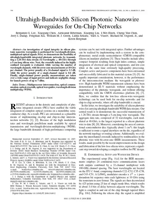
398IEEE PHOTONICS TECHNOLOGY LETTERS,VOL.20,NO.6,MARCH 15,2008Ultrahigh-Bandwidth Silicon Photonic NanowireWaveguides for On-Chip NetworksBenjamin G.Lee,Xiaogang Chen,Aleksandr Biberman,Xiaoping Liu,I-Wei Hsieh,Cheng-Yun Chou,Jerry I.Dadap,Fengnian Xia,William M.J.Green,Lidija Sekaric,Yurii A.Vlasov,Richard M.Osgood,Jr.,andKeren BergmanAbstract—An investigation of signal integrity in silicon pho-tonic nanowire waveguides is performed for wavelength-division-multiplexed optical signals.First,we demonstrate the feasibility of ultrahigh-bandwidth integrated photonic networks by transmit-ting a 1.28-Tb/s data stream (32wavelengths 40-Gb/s)through a 5-cm-long silicon wire.Next,the crosstalk induced in the highly confined waveguide is evaluated,while varying the number of wavelength channels,with bit-error-rate measurements at 10Gb/s per channel.The power penalty of a 24-channel signal is 3.3dB,while the power penalty of a single-channel signal is 0.6dB.Finally,single-channel power penalty measurements are taken over a wide range of input powers and indicate negligible change for launch powers of up to 7dBm.Index Terms—Multiprocessor interconnection,optical commu-nication,optical crosstalk,optical waveguides,wavelength-division multiplexing (WDM).I.I NTRODUCTIONRECENT advances in the density and complexity of pho-tonic integrated circuits (PICs)have enabled the viable integration of complete optical systems on a monolithic semi-conductor chip.As a result,PICs are envisioned as a plausible means of implementing on-chip and chip-to-chip intercon-nection networks [1],[2].Because of the high modulation rates and wavelength parallelism made available by optical transmission and wavelength-division-multiplexing (WDM),the large bandwidth demands of high-performance computingManuscript received September 27,2007;revised December 10,2007.The work of B.G.Lee,A.Biberman,and K.Bergman was supported by the National Science Foundation (NSF)under Grant CCF-0523771and Grant ECS-0725707.The work of X.Chen,X.Liu,I-W.Hsieh,C.-Y.Chou,J.I.Dadap,and R.M.Osgood,Jr.was supported by the Department of Defense (DoD)Small Business Technology Transfer (STTR)under Con-tract FA9550-05-C-1954and by the Air Force Office of Scientific Research (AFOSR)under Grant FA9550-05-1-0428.The work of F.Xia,W.M.J.Green,L.Sekaric,and Y .A.Vlasov was supported by the Defense Advanced Research Projects Agency (DARPA)under Grant N00014-04-C-0455.B.G.Lee,X.Chen, A.Biberman,X.Liu,I-W.Hsieh,C.-Y.Chou,R.M.Osgood,Jr.,and K.Bergman are with the Department of Elec-trical Engineering,Columbia University,New York,NY 10027USA (e-mail:benlee@;oliver@;ab2795@;xl2165@;ih2109@;cc2535@;osgood@;bergman@).J.I.Dadap is with the Department of Applied Physics and Applied Mathematics,Columbia University,New York,NY 10027USA (e-mail:dadap@).F.Xia,W.M.J.Green,L.Sekaric,and Y. A.Vlasov are with the IBM Thomas J.Watson Research Center,Yorktown Heights,NY 10598USA (e-mail:fxia@;wgreen@;lidija@;yvlasov@).Digital Object Identifier 10.1109/LPT.2008.916912systems can be met with integrated optics.Further advantages can be realized by implementing such a system in the com-plementary metal–oxide–semiconductor (CMOS)-compatible silicon-on-insulator platform [3].These benefits include ultra-compact footprint resulting from high index contrast,simple integration of electrical and optical components,and low-cost while at the same time extremely high-quality plex active and passive components have been envisioned and successfully fabricated in this material system [3]–[5].An equally important consideration,however,is the performance of the interconnection medium:the waveguide or photonic wire .High-bandwidth WDM transmission schemes have been demonstrated in III–V materials without emphasizing the importance of the photonic waveguide,and without offering compatibility with the CMOS electronics platform [6],[7].Here,we confirm that the low-loss silicon-wire-waveguide technology can be used both for on-chip networks and for chip-to-chip networks,where off-chip bandwidth is crucial.In this letter,we investigate the suitability of silicon photonic wires for carrying ultrahigh-bandwidth WDM data streams.Our central result is to demonstrate the successful transmission of a 1.28-Tb/s stream through a 5-cm-long wire waveguide.The aggregate data rate,composed of 32wavelengths,each mod-ulated at 40-Gb/s,is the largest reported in a silicon photonic wire to date [8],[9].Moreover,considering the area of conven-tional semiconductor dice (typically about 1cm ),this length is sufficient to route a signal anywhere on the die,regardless of the network topology or routing scheme.Additionally,we eval-uate the interchannel crosstalk induced by nonlinearities in the photonic wire with bit-error-rate (BER)measurements.These results,made possible by the recent improvements in the design and fabrication of the low-loss silicon wires,represent a signifi-cant step toward developing a complete toolbox for PIC design.II.E XPERIMENTAL S ETUP AND W A VEGUIDE D EVICE The experimental setup [Fig.1(a)]for the BER measure-ments employs 24continuous-wave communications lasers with outputs combined by a 32-channel multiplexer with 100-GHz channel spacing.The laser wavelengths are located on theITU -band,comprising channels C22–C32,C35–C38,and C43–C51.ALiNbO modulator encodesapseu-dorandom bit sequence onto each lightwave at 10Gb/s using the nonreturn-to-zero format.The signals are then decorrelated by 425ps/nm using 25km of single-mode fiber,which results in about 3.4bits of delay between adjacent wavelengths.The light is coupled in and out of the chip through tapered fibers [Fig.1(b)].Following the silicon chip,the signal is amplified1041-1135/$25.00©2008IEEELEE et al.:ULTRAHIGH-BANDWIDTH SILICON PHOTONIC NANOWIRE WA VEGUIDES FOR ON-CHIP NETWORKS399Fig.1.(a)Diagram of the experimental setup,(b)schematic of the fiber cou-pling and wire waveguide layout,and (c)scanning electron microscope (SEM)image of the silicon photonic wire cross section.by an erbium-doped fiber ampli fier (EDFA),after which some of the power is tapped for monitoring on an optical spec-trum analyzer (OSA).One wavelength channel is selected for measurement using a tunable filter,which is followed by an at-tenuator and a receiver module consisting of a p-i-n photodiode (PIN),transimpedance ampli fier (TIA),and limiting ampli fier (LA).The detected signal is evaluated with a communications signal analyzer (CSA)and a BER tester (BERT),which is synchronized directly to the pulse pattern generator (PPG)by a 10-GHz clock source.Polarization controllers (PCs)are used throughout.The setup for the 1.28-Tb/s demonstration employs 32chan-nels,C21(1560.61nm)through C52(1535.82nm),each modu-lated at 40Gb/s and decorrelated by 94ps/nm in 5.5km of fiber,resulting in about 3bits of delay between adjacent wavelengths.In addition,a 40-Gb/s PIN-TIA replaces the former 10-Gb/s PIN-TIA-LA.The silicon photonic wire is a single-mode waveguide with a height of 220nm and a width of 520nm [Fig.1(c)].The de-vice was fabricated using the CMOS production line at the IBM T.J.Watson Research Center.Each end has an inverse-taper mode converter covered with index matching polymer,which al-lows ef ficient coupling(1dB per facet)[10].The 5-cm length was achieved by snaking the wire across the chip [Fig.1(b)],making a total of 2490-bends with bending radii of6.5m.Dispersion and nonlinear parameters of the wire are similar to those shown in previous work [11]–[13].III.E XPERIMENTS AND R ESULTSFirst,we con firm the feasibility of ultrahigh-bandwidth net-works utilizing silicon photonic wires by generating a 1.28-Tb/s data stream,composed of 3240-Gb/s wavelength channels,and propagating the stream through the 5-cm wire.The input spec-trum and a selection of eye diagrams before and after the wave-guide propagation are shown (Fig.2).A major source of degra-dation results from the ampli fication required to compensate the on-chip propagation loss(3dB/cm).It should also be noted that the polarization states of the 32channels,which are aligned prior to the multiplexer,drift slightly in the decorrelator by various amounts.Therefore,for the 40-Gb/s measurements only,the state of the PCprecedingFig.2.(a)Input spectrum for the 1.28-Tb/s signal with a resolution bandwidth of 0.06nm;(b)input (top)and output (bottom)eye diagrams for channels (from left to right)C23,C28,C46,and C51with 10ps/div.the polarization-sensitive photonic wire was optimized for each channel while viewing the eye diagram.This drifting of the states of polarization across the wavelength channels,however,arises from the manner in which we simultaneously modulate the entire spectrum with a single modulator,and then decorre-late the channels to emulate 32independent streams.In actual network implementations where independent data are encoded onto each channel separately before wavelength-multiplexing,this problem does not exist,because only a short length of fiber is required between the multiplexing and the fiber-to-chip coupling.The second experiment characterizes the crosstalk be-tween wavelength channels in the photonic wire with a peak launch power (i.e.,“1”bit power)of approximately 6dBm per channel.The BER characteristics are evaluated at 10Gb/s rather than 40Gb/s,because a 40-Gb/s BERT was not available.Receiver sensitivity curves are taken before and after propa-gation through the 5-cm wire for a single probe wavelength,C36(1548.51nm).The observed power penalty is 0.6dB (Fig.3).Then,20additional wavelength channels are enabled and passed through the silicon wire alongside the probe,with the nearest channel being greater than 3nm in wavelength from the probe.A degradation of 1.5dB in the sensitivity curve ata BERofis noticed.Next,three more wavelengths are enabled,totaling 24wavelength channels or 240Gb/s.These wavelengthsoccupy -band channels adjacent to the probe (C35,C37,and C38).The additional crosstalk from these channels further increases the power penalty by 1.1dB.Finally,a sensitivity curve is taken for the 24-channel signal before entering the photonic wire.The resulting 24-channel power penalty is 3.3dB.Given the length of the silicon photonic wire and the number of channels in the input signal,the measured penalty is quite tolerable.The reasonable overlap between the two extreme back-to-back curves (1-channel and 24-channels)in Fig.3indicates that the measured degradation is a result of crosstalk in the silicon wire,rather than crosstalk occurring elsewhere in the setup (e.g.,the EDFA).400IEEE PHOTONICS TECHNOLOGY LETTERS,VOL.20,NO.6,MARCH 15,2008Fig.3.BER curves at 10Gb/s showing wavelength crosstalk in a 5-cm wire waveguide with symbols denoting single-(),21-( ),and 24-channel ()WDM signals.Measurements are taken for signals going through (solid lines,filled symbols)and bypassing (dashed lines,open symbols)thewire.Fig.4.BER curves at 10Gb/s for a single wavelength channel injected into the 5-cm wire waveguide with more than 7dBm of peak power.Measurements are taken for signals going through ()and bypassing ()the wire.Previously,self-phase modulation (SPM)has been observed in silicon wires using picosecond pulses [12].Typically,the in-jected powers required to observe SPM are a few tens of mil-liwatts with 0.4-cm-long wires.It is important to consider the power penalty induced when high-power signals are launched into much longer wires.Fig.4shows the BER curves for a single wavelength at 1550nm with a peak (i.e.,“1”bit)power of more than 7dBm injected into the wire.The resulting 0.5-dB power penalty is within the experimental error of the previous single-channel measurement (0.6dB,shown in Fig.3),taken with a much lower launch power.(Of the seven BER curves shown in Figs.3and 4,the average of the root-mean-square (rms)errors for each curve is 0.1dB with a maximum rms error of 0.2dB.)This result con firms consistent power penalties over an input power dynamic range of more than 10dB.IV .C ONCLUSIONWe have successfully demonstrated the transport of ter-abit-per-second-scale WDM data signals using silicon photonic wires over suf ficient distances for any on-chip network.An extensive investigation of the crosstalk is performed using 10-Gb/s channels.The interchannel nonlinear processes (e.g.,cross-phase modulation and four-wave mixing)are more no-ticeable than intrachannel processes (e.g.,SPM)for signals with many wavelengths.Yet even in a 5-cm-long dense WDM 10-Gb/s link,the wire exhibits only a 3.3-dB power penalty ata BERof.Finally,single-channel 10-Gb/s measurements with input powers ranging across approximately 13dB,show no change in power penalty,indicating there could be enough power margin to meet at least a single-channel network ’s optical power budget.A CKNOWLEDGMENTThe authors would like to thank Dr.N.C.Panoiu for helpful discussions on nonlinear optics.R EFERENCES[1]ler,“Rationale and challenges for optical interconnects toelectronic chips,”Proc.IEEE ,vol.88,no.6,pp.728–749,Jun.2000.[2]A.Shacham,K.Bergman,and L.P.Carloni,“On the design of aphotonic network-on-chip,”in works-On-Chip (NOCS),Princeton,NJ,May 2007,Paper 2.1.[3]M.Lipson,“Guiding,modulating,and emitting light on silicon-chal-lenges and opportunities,”J.Lightw.Technol.,vol.23,no.12,pp.4222–4238,Dec.2005.[4]B.G.Lee,B.A.Small,Q.Xu,M.Lipson,and K.Bergman,“Charac-terization of a 424Gb/s parallel electronic bus to WDM optical link silicon photonic translator,”IEEE Photon.Technol.Lett.,vol.19,no.7,pp.456–458,Apr.1,2007.[5]F.Xia,L.Sekaric,and Y.Vlasov,“Ultracompact optical buffers on asilicon chip,”Nature Photon.,vol.1,no.1,pp.65–71,Jan.2007.[6]M.Arai,T.Kondo,A.Matsutani,T.Miyamoto,and F.Koyama,“Growth of highly strained GaInAs –GaAs quantum wells on patterned substrate and its application for multiple-wavelength vertical-cavity surface-emitting laser array,”IEEE J.Sel.Topics Quantum Electron.,vol.8,no.4,pp.811–816,Jul.2002.[7]R.Nagarajan et al.,“Large-scale photonic integrated circuits forlong-haul transmission and switching,”w.,vol.6,no.2,pp.102–111,Feb.2007.[8]X.Chen et al.,“Demonstration of 300Gbps error-free transmissionof WDM data stream in silicon photonic wires,”in sers Electro-Optics (CLEO),Baltimore,MD,May 2007,Paper CTuQ5.[9]B.G.Lee et al.,“Ultrahigh-bandwidth WDM signal integrity in sil-icon-on-insulator nanowire waveguides,”in sers Electro-Op-tics Soc.Annu.Meeting (LEOS),Lake Buena Vista,FL,Oct.2007,Paper WG2.[10]S.McNab,N.Moll,and Y.Vlasov,“Ultra-low loss photonic integratedcircuit with membrane-type photonic crystal waveguides,”Opt.Ex-press ,vol.11,no.22,pp.2927–2939,Nov.3,2003.[11]E.Dulkeith,F.Xia,L.Schares,W.M.J.Green,and Y.A.Vlasov,“Group index and group velocity dispersion in silicon-on-insulator photonic wires,”Opt.Express ,vol.14,no.9,pp.3853–3863,May 1,2006.[12]E.Dulkeith,Y.A.Vlasov,X.Chen,N.C.Panoiu,and R.M.Osgood,Jr.,“Self-phase-modulation in submicron silicon-on-insulator photonic wires,”Opt.Express ,vol.14,no.12,pp.5524–5534,Jun.12,2006.[13]I.-W.Hsieh et al.,“Ultrafast-pulse self-phase modulation and third-order dispersion in Si photonic wire-waveguides,”Opt.Express ,vol.14,no.25,pp.12380–12387,Dec.11,2006.。
Optoelectronics and Photonics Principles and Practice English Edition Second Edition Course Design IntroductionThe field of optoelectronics and photonics has gned significant attention in both the scientific and engineering communities due to its potential for creating high-speed, high-bandwidth, and low-power devices. The goal of this course is to provide students with an understanding of the principles and practices of optoelectronics and photonics, as wellas prepare them for advanced research and development in the field.Course ObjectivesUpon completion of this course, students will be able to:•Understand the principles and properties of electromagnetic waves•Describe the fundamental concepts of light propagation and interactions with matter•Analyze the properties of optical components such as lenses, mirrors, and filters•Understand the principles and operations of optical detectors and sources•Describe the basics of fiber optics and opticalcommunication systems•Analyze the principles and applications of photonics in various fieldsCourse StructureThe course will consist of lectures, discussions, and laboratory experiments. The course will cover the following topics:Part I: Fundamentals of Optics and Electromagnetic Waves1.Introduction to Optoelectronics and Photonics2.Electromagnetic Waves and Optics3.Geometrical Optics4.Wave And Ray Propagation in Anisotropic MediaPart II: Optical Components and Devices5.Optical Components6.Polarization of light7.Detectors and Sources of LightPart III: Introduction to Photonics8.Fundamentals of Photonicssers, fiber optics, and optical communication systems10.Biophotonics and ApplicationsLaboratory ExperimentsThe laboratory experiments will allow students to apply the concepts learned in class and gn hands-on experience with various optical components and devices. The following experiments will be performed:1.Reflection and Refraction of Light using Lenses and Mirrors2.Polarization of Light and Measurement of Optical Activity3.Measurement of Band Gap in Semiconductor Materials4.Analysis of Optical Filters using Spectrophotometer5.Study of Optical Fiber Characteristics using Optical TimeDomn Reflectometer6.Design and Characterization of a Laser Diode and OpticalCommunication SystemConclusionThis course provides a comprehensive understanding of the principles and practices of optoelectronics and photonics. Through lectures, discussions, and laboratory experiments, students will gn a deep understanding of the fundamentals of optics and electromagnetic waves, optical components and devices, and photonics applications. Upon completion of this course, students will be equipped with the knowledge and skills necessary for advanced research and development in this field.。
雷达科学与技术!"d"$ Science and Technology第2期2021年4月Vol19No2April2021DOI : 10. 3969". issn. 1672-2337. 2021. 02. 012微波光子雷达组网技术范北辰,杨 悦,马 丛,王祥传,张方正,潘时龙(南京航空航天大学雷达成像与微波光子技术教育部重点实验室,江苏南京211106)摘 要:雷达组网是目前雷达领域的研究热点之一。
通过对空间区域进行多角度、多频段、多域协同探测,雷达组网能够获取目标的多维度信息,并利用数据的融合处理进一步地提升系统的目标探测与识别能。
随着系统对信号质量、信链路带宽以及系统同步精度等 的日 ,基于微波光子技术实现信号产生、传输和处理的雷达组网 获得研究者的关注。
本文分析了微波光子雷达组网关键技术的工作原理,介绍了 来 外微波光子雷达组网的发展现状,并探讨了其未来的演进方向。
关键词:雷达组网;微波光子雷达;MIM0雷达;分布式相参雷达中图分类号:TN957.52;TN958文献标志码:A 文章编号:1672-2337(2021)02-0195-13Microwave Photonic Radar NetworkFAN Beichen, YANG Yue, MA Cong, WANG Xiangchuan, ZHANG Fangzheng, PAN Shilong(Key Laboratory of Radar Imaging and Microwave Photonics , Ministry of Education , Nanjing University of Aeronautics and Astronautics , Nanjing 211106, China')Abstract :Radar network, one of the hot topics in the area of radar , can perform multi-angle, multi-bandandmulti-domainco l aborativedetectionoftargets(Thankstothecapabilityofmulti-dimensionalinformationfu-sion, radar network can greatly improve the target detection and recognition performance. With the increasingdemandsofradarnetworkperformanceintermsofbandwidth $distanceandsynchronizationaccuracyofinforma- tiontransmissionlinks $microwavephotonicradarnetworkisgaining greata t entionfrom researchers $onaccount of its capability of high-quality microwave signal generation $processing and phase-stable transmission.Thispaperanalyzeskeytechnologiesinmicrowavephotonicradarnetworks $reviewstherecentadvancementand discussesitspossibleresearchdirectioninthefuture.Key words : radar network & micro w ave photonic radar & MIMO radar ; distributed coherent radar引言雷达组网,通过对多部雷达合理:和优化部署,增加了系统的自由度,实现了对覆盖区的截获、目标探测等能力的大幅提升。
摘要摘要随着固定网络和无线接入网络对带宽需求的急剧增长,光载射频通信(radio-over-fiber,RoF)技术因其在系统容量、带宽和移动性方面的优势受到了越来越广泛的关注。
其中光生毫米波技术是RoF系统的关键技术之一。
本论文主要对多倍频毫米波光学产生技术及其传输性能进行了研究。
论文首先介绍了光生毫米波技术的基本原理及关键技术,然后提出了三种新型基于外调制器产生多倍频毫米波的方案,并对基于毫米波的RoF传输系统进行了研究,具体研究工作如下:1.提出了三种基于外调制的多倍频光生毫米波技术方案。
方案一,基于一个集成的偏振复用双平行马赫曾德尔调制器(PDM-DPMZM)通过合理的设置射频驱动信号、偏振控制器的角度以及调制器的工作点来产生八倍频光学毫米波信号。
该方案不需要任何光或电的滤波器,并且该方案对调制指数没有非常严格的要求;仿真结果显示,当调制指数设置在一个合理的范围(4.29~4.6),可以由一个10GHz的射频驱动信号产生80GHz的毫米波信号,产生的电谱非常纯净,信噪比(SNR)达到了51.3dB;方案二,基于两个并联的偏振调制器(PolM)实现十二倍频光学毫米波信号。
该方案中偏振调制器(PolM)具备高的消光比并且不需要直流偏置,从而避免了直流偏置漂移问题,保证了系统良好的稳定性。
方案三,基于两个级联的双偏振调制器(DPol-MZM),不使用任何光和电的滤波器产生二十四倍频光学毫米波信号。
通过合理的设置射频驱动信号、双偏振调制器(DPol-MZM)的工作点、光信号的偏振方向,产生了正负十二阶光边带。
通过仿真实现了由一个5GHz的射频驱动信号产生120GHz的毫米波信号2.提出了一种基于集成的双偏振调制器(DPol-MZM)产生二倍频微波光子移向器的方案,仿真结果显示,通过简单的调节光的偏振方向,从检偏器输出的毫米波信号就可以实现0-360○相移,并且在相移调节过程中,信号的幅度始终保持不变。
物理光学英语The Fascinating World of Physical OpticsLight is a fundamental aspect of our universe, and the study of its behavior and interactions with matter is known as physical optics. This field of study encompasses a wide range of phenomena, from the simple reflection and refraction of light to the complex interactions of light with various materials and structures. In this essay, we will delve into the captivating world of physical optics and explore some of its key concepts and applications.At the heart of physical optics is the understanding of the nature of light itself. Light is a form of electromagnetic radiation, characterized by its wavelength and frequency. The wave-particle duality of light is a fundamental principle in quantum mechanics, which states that light exhibits both wave-like and particle-like properties. This dual nature of light is the foundation for many of the phenomena observed in physical optics.One of the most fundamental concepts in physical optics is the behavior of light as it interacts with different materials. When light encounters a surface, it can undergo reflection, refraction, orabsorption, depending on the properties of the material. Reflection occurs when light bounces off a surface, and the angle of reflection is equal to the angle of incidence. Refraction, on the other hand, occurs when light bends as it passes from one medium to another with a different refractive index. This phenomenon is responsible for the apparent bending of objects when viewed through water or a prism.Another important aspect of physical optics is the interference of light. When two or more light waves interact, they can either constructively or destructively interfere, resulting in a pattern of bright and dark regions. This phenomenon is the basis for many optical devices, such as lasers and holographic displays. Interference can also be used to measure small distances and detect the presence of thin films or coatings on surfaces.Diffraction is another fascinating concept in physical optics. When light encounters an obstacle or an aperture, it can bend and spread out, creating a diffraction pattern. This effect is particularly noticeable when light passes through a small slit or a grating, and it is the underlying principle behind many optical instruments, such as telescopes and microscopes.In addition to these fundamental concepts, physical optics also encompasses the study of polarization, which describes the orientation of the electric field in a light wave. Polarization can beused to study the structure and properties of materials, as well as to create specialized optical devices, such as liquid crystal displays (LCDs) and optical filters.The applications of physical optics are vast and varied, spanning a wide range of industries and fields of study. In telecommunications, for example, optical fibers are used to transmit data over long distances, taking advantage of the low-loss and high-bandwidth properties of light. In medicine, lasers are used for a variety of diagnostic and therapeutic procedures, such as eye surgery and cancer treatment. In the field of astronomy, telescopes and other optical instruments are essential for observing and studying the universe.Furthermore, the principles of physical optics are also applied in the development of new materials and technologies. For instance, the study of photonic crystals, which are materials with a periodic structure that can control the flow of light, has led to the creation of novel optical devices and sensors.In conclusion, physical optics is a fascinating and dynamic field of study that encompasses a wide range of phenomena and applications. From the fundamental principles of light behavior to the cutting-edge developments in optical technologies, the study of physical optics continues to push the boundaries of ourunderstanding of the physical world and the universe around us. As we continue to explore and unravel the mysteries of light, the possibilities for new discoveries and innovations in this field are truly limitless.。
微波光子信道化接收技术英语Microwave Photonic Channelized Reception Technology.Microwave photonic technology, which converts microwave signals into optical signals for transmission, has emerged as a key enabler for high-speed and high-bandwidth communication networks. This technology offers significant advantages, including ultra-high bandwidth, large capacity, and low loss. Among the crucial components of microwave photonic systems, microwave photonic channelized receivers play a pivotal role in enabling high-performance communication networks.The microwave photonic channelized receiver is a device that converts photonic signals back into microwave signals. Its operation relies on the use of optical components, such as fibers and gratings, along with microwave componentslike filters and delay lines. The basic principle involves the conversion of optical signals to microwave signals using optical devices, followed by signal conditioning anddemodulation using microwave components.The structure of a microwave photonic channelized receiver typically comprises several key elements, including a light source, optical modulator, optical detector, optical fiber delay line, and microwave filter. The light source generates the optical signal, which is then modulated by the optical modulator. The modulated optical signal is then converted into an electrical signal by the optical detector. The optical fiber delay line introduces a time delay in the signal, while the microwave filter removes any unwanted signals. Commonly used optical detection technologies include photodiodes and photomultipliers.A significant advantage of microwave photonic channelized receivers is their ability to overcome the bandwidth limitations of traditional electronic devices. Due to the enormous bandwidth capabilities of optical components, these receivers can significantly expand the frequency detection range. Furthermore, they enable the miniaturization of surveillance equipment, reducing itssize, weight, and power consumption.The core concept of photonic channelized receivers, similar to traditional channelized receivers, is thedivision of the wideband spectrum into multiple narrowband sub-bands. Each sub-band is then processed individually using heterodyning techniques. However, in the case of photonic channelized receivers, this division andprocessing are performed in the optical domain. Essentially, optical components are used to emulate the functionality of analog or digital filters in traditional electronic systems.Microwave photonic channelized arrays, which convert wideband microwave-modulated optical signals into multiple narrowband modulated optical signals through optical filtering, are a key component of microwave photonic channelized receivers. By combining high-speed electro-optic modulators and low-speed photodetector arrays, microwave photonic channelized receivers can be realized. This approach overcomes the limitations of traditional microwave photonic links, which typically involve direct photoelectric conversion of wideband modulated opticalsignals into radio frequency electrical signals for processing.The application of microwave photonic channelizers, the optical processing elements within microwave photonic systems, is diverse and widespread. Initially, they found their application in military domains, particularly in radar and electronic warfare systems, to meet the demands of modern warfare. However, their potential applications are not limited to military use cases. Civilianapplications in areas like satellite communications, wireless networks, and radio astronomy are also being explored.In conclusion, microwave photonic channelized reception technology offers a promising approach to address the challenges posed by the increasing bandwidth requirements of modern communication systems. By leveraging the unique properties of optical components, it enables therealization of high-performance communication networks with expanded frequency detection capabilities, reduced equipment size, weight, and power consumption. Astechnology continues to evolve, the potential applications and impact of microwave photonic channelized receivers will only grow.。
瞬时频率测量(IFM ,instantaneous frequencymeasurement )技术是指在脉冲持续的短周期内对被测信号的频率进行快速测量[1]。
针对IFM 技术的研究,早期以电子学方法为主,然而,随着测量要求的提高,“电子瓶颈”以及电磁干扰问题阻碍了该技术的发展,因此,在研究中引入了微波光子学。
微波光子辅助的IFM 系统相比传统电子学方法具有其独特优势:(1)测量范围受带宽限制较小,可实现小型化超宽带微波信号的分析和检测;(2)抗电磁干扰特性能够提高测量的隐秘性,有效保护测量系统。
目前提出的微波光子辅助的IFM 系统按映射方式可大致划分为频率-空间、频率-时间和频率-幅度三类映射。
主要对基于频率-幅度映射的IFM 系统进行分类比较,并进一步引申到高精度可调谐测量范围的IFM 技术研究,重点总结了一种单光源无滤波结构的IFM 新方案。
1IFM 系统的分类与技术要点1.1频率-空间映射频率-空间映射方案是利用光载波通过一些不·测试、试验与仿真·微波光子辅助的瞬时频率测量技术研究进展李月琴,裴丽,宁提纲,王一群,袁瑾,李晶(北京交通大学光波技术研究所,北京100044)摘要:微波光子辅助的瞬时频率测量(IFM )系统具有高时间带宽积、低功率损耗、轻系统质量以及抗电磁干扰等巨大优势。
对目前国内外研究的IFM 系统按照频率-空间、频率-时间和频率-幅度三种映射方式进行分类介绍,主要归纳比较了具有频率-幅度映射关系的IFM 系统,针对其中存在的测量范围和测量精度之间的互换(Trade -off )问题,进一步引申到研究高精度可调谐测量范围的IFM 技术,并对目前相关领域的研究进行了追踪报道。
关键词:瞬时频率测量;微波光子;频率-幅度映射中图分类号:TN914.2文献标识码:A文章编号:1673-1255(2014)-04-0076-05Research Progress in Microwave Photonic -assisted Instantaneous FrequencyMeasurement TechnologyLI Yue -qin,PEI Li,NING Ti -gang,WANG Yi -qun,YUAN Jin,LI Jing(Institute of Lightwave Technology,Beijing Jiaotong University,Beijing 100044,China)Abstract:Microwave photonic -assisted instantaneous frequency measurement (IFM)system has many advan ⁃tages such as high time -bandwidth product,low power consumption,light weight and anti -electromagnetic interfer ⁃ence.Domestic and foreign IFM systems are introduced respectively according to three kinds of mapping modes such as frequency -space,frequency -time and frequency -amplitude.And IFM system with frequency -amplitude map ⁃ping relationship is mainly concluded and compared.According to the trade -off problem between measurement range and accuracy,IFM researching technology with high accuracy and tunable measurement range is further pre ⁃sented.And the current researches in the fields are reported.Key words:instantaneous frequency measurement;microwave photonic;frequency -amplitude mapping第29卷第4期2014年8月光电技术应用ELECTRO -OPTIC TECHNOLOGY APPLICATIONVol.29,No.4August ,2014收稿日期:2014-06-20基金项目:国家自然科学基金(61275076)资助课题作者简介:李月琴(1989-),女,广西北海人,博士,主要研究方向为微波光子、RoF 等.第4期同的特殊光学通道来获得微波信号频率的方法。
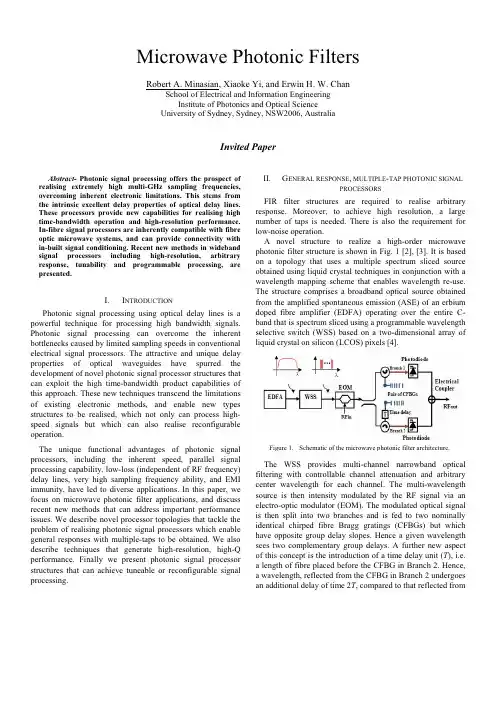
Microwave Photonic Filters Robert A. Minasian, Xiaoke Yi, and Erwin H. W. Chan School of Electrical and Information EngineeringInstitute of Photonics and Optical ScienceUniversity of Sydney, Sydney, NSW2006, AustraliaInvited PaperAbstract- Photonic signal processing offers the prospect of realising ex tremely high multi-GHz sampling frequencies, overcoming inherent electronic limitations. This stems from the intrinsic ex cellent delay properties of optical delay lines. These processors provide new capabilities for realising high time-bandwidth operation and high-resolution performance. In-fibre signal processors are inherently compatible with fibre optic microwave systems, and can provide connectivity with in-built signal conditioning. Recent new methods in wideband signal processors including high-resolution, arbitrary response, tunability and programmable processing, are presented.II.G ENERAL RESPONSE, MULTIPLE-TAP PHOTONIC SIGNALPROCESSORSFIR filter structures are required to realise arbitrary response. Moreover, to achieve high resolution, a large number of taps is needed. There is also the requirement for low-noise operation.A novel structure to realize a high-order microwave photonic filter structure is shown in Fig. 1 [2], [3]. It is based on a topology that uses a multiple spectrum sliced source obtained using liquid crystal techniques in conjunction with a wavelength mapping scheme that enables wavelength re-use. The structure comprises a broadband optical source obtained from the amplified spontaneous emission (ASE) of an erbium doped fibre amplifier (EDFA) operating over the entire C-band that is spectrum sliced using a programmable wavelength selective switch (WSS) based on a two-dimensional array ofI.I NTRODUCTIONPhotonic signal processing using optical delay lines is a powerful technique for processing high bandwidth signals. Photonic signal processing can overcome the inherent bottlenecks caused by limited sampling speeds in conventional electrical signal processors. The attractive and unique delay properties of optical waveguides have spurred the development of novel photonic signal processor structures that can exploit the high time-bandwidth product capabilities of this approach. These new techniques transcend the limitations of existing electronic methods, and enable new types structures to be realised, which not only can process high-speed signals but which can also realise reconfigurable operation.The unique functional advantages of photonic signal processors, including the inherent speed, parallel signal processing capability, low-loss (independent of RF frequency) delay lines, very high sampling frequency ability, and EMI immunity, have led to diverse applications. In this paper, we focus on microwave photonic filter applications, and discuss recent new methods that can address important performance issues. We describe novel processor topologies that tackle the problem of realising photonic signal processors which enable general responses with multiple-taps to be obtained. We also describe techniques that generate high-resolution, high-Q performance. Finally we present photonic signal processor structures that can achieve tuneable or reconfigurable signal processing.Figure 1.Schematic of the microwave photonic filter architecture.The WSS provides multi-channel narrowband optical filtering with controllable channel attenuation and arbitrary center wavelength for each channel. The multi-wavelength source is then intensity modulated by the RF signal via an electro-optic modulator (EOM). The modulated optical signal is then split into two branches and is fed to two nominally identical chirped fibre Bragg gratings (CFBGs) but which have opposite group delay slopes. Hence a given wavelength sees two complementary group delays. A further new aspect of this concept is the introduction of a time delay unit (T), i.e.a length of fibre placed before the CFBG in Branch 2. Hence, a wavelength, reflected from the CFBG in Branch 2 undergoes an additional delay of time 2T, compared to that reflected fromFig. 2. Measured RF response for the 158-tap microwave photonic filter.Branch 1. The reflected and delayed signals are then detected by photodetectors in each branch and are combined at an electrical combiner.Experimental results for a high-order FIR microwave photonic filter designed to realize 158 taps, are shown in Fig. 2. The results demonstrate a high-resolution microwave photonic filter at 6.67 GHz, with a measured 3 dB bandwidth of 37.5 MHz. The high-resolution filter response comprises 158 taps, which to our knowledge is the highest number of taps for a microwave photonic FIR filter reported to date.III. H IGH -RESOLUTION , HIGH -Q PHOTONIC SIGNALPROCESSORS Many applications require high frequency selectivity and high-Q bandpass filtering. This generically requires many taps in the impulse response of the discrete time signal processor. Filters based on a recursive optical delay line can generate a large number of optical taps using simple structures.Conventional high-resolution, high-Q photonic processors [5]-[6], are principally limited by the excessive phase induced intensity noise (PIIN) that is generated by the optical interference in summing the multiple delayed optical signals. To obtain a robust transfer characteristic irrespective of environmental perturbations, conventional approaches have required the use of an incoherent approach, in which the coherence of the light source is made smaller than the minimum delay time of the processor. However, when the light from the same optical source is delayed in different optical paths and then re-combined together in the optical domain, the phase noise of the light is converted to intensity noise [7], and this problem compounds for recursive delay lines that have a large number of taps. This is important, because high-resolution processors require a large number of taps, thus efforts to increase the resolution of the processor are accompanied by an increase in the dominant PIIN noise.A structure for realising a high-Q processor with extremely low PIIN generation is based on a frequency-shifting recirculating delay line (FS-RDL) [1]. The central idea is to inject modulated light from a laser, into a frequency-shifting loop. Each recirculation imposes a frequency shift on the light and produces a time delay T , and constitutes a tap in the impulse response. This processor structure can create many taps because numerous recirculations can occur. However, the most important point in this concept is that this method recombines signals at the photodetector at different wavelengths, so that the phase induced intensity noise appears at the beat frequency corresponding to the frequency shift, which falls outside the photodetector bandwidth and is automatically filtered out. This enables both a large number of taps to be generated, and also suppresses the dominant PIIN noise. Moreover, since every tap generated by the structure will have a different wavelength, the filter is essentially coherence free, enabling the use of a narrow linewidth telecommunications-type laser as the optical source for the system. Results have shown a high-Q filter with a large PIIN reduction [8]. Recently, Q values of 407 have beenexperimentally demonstrated.An extension to this concept to realise a structure that can modify the tap amplitudes to enable windowing to be applied to the resultant impulse response [9], is shown in Fig. 3. In the time domain, the taps are separated by a constant time delay corresponding to the recirculation time. In the optical frequency domain, the taps are separated by a constant optical frequency determined by the frequency of the optical frequency shifter. Since the taps have different optical frequencies, a wavelength dependent element at the output of the loop can be used to control the tap amplitudes, thus offering the means to alter the signal processor impulse response shape. By designing the spectrum shape of the wavelength dependent element together with the system parameters of the FS-RDL, windowing is applied to the impulse response of the signal processor. Hence, a high performance bandpass filter response can be realised. Note that the structure shown in Fig. 3 is an FIR signal processor even though it is formed by a recirculating structure.Optical frequency shifterFig. 3.Topology of the high performance coherence-free microwavephotonic signal processor.Fig. 4 shows experimentally measured results thatdemonstrate high-resolution bandpass filter operation, with a shape factor of only 3.1, and a bandpass filter stopband attenuation of over 70 dB.Optical couplerfilter: measured (solid), predicted (dots).In addition to enabling a large number of tap to begenerated using a simple configuration for high-resolutionsignal processing, this signal processor has no coherentinterference and phase noise limitations, and offers coherence-free, high-resolution, high-performance filtering operation.IV.P ROGRAMMABLE C OMPLEX COEFFICIENT T UNEABLEAND RECONFIGURABLE SIGNAL PROCESSORFilters that can be synthesized with complex-coefficientsoffer the highly desirable advantage of enabling the filtercentre frequency to be tuned without changing its responseshape, its basic time delay, or its free-spectral range (FSR).A new all-optical microwave photonic filter structure thatcan realize arbitrary programmable complex coefficients,multiple taps, and which offers shape-invariant frequencytuning over the full FSR range [10], is shown in Fig. 5. It isbased on a new optical RF phase shifter that uses aprogrammable wavelength processor (PWP) comprising atwo-dimensional array of LCoS pixels [4], which enablessingle-sideband (SSB) modulation and the imparting ofarbitrary optical phase shifts from 0 to 360q to the carriers andSSB sidebands, to be achieved simultaneously.Fig. 5. Structure of the microwave photonic signal processor.The PWP performs two functions. The first is to create anarray of SSB modulations by eliminating one sideband of eachoptical carrier, as shown in Fig. 5. The second function of thePWP is to impress phase shifts on the optical carriers and theSSB sidebands,which are directly translated to the RF signalafter detection. The optical transfer function including bothoptical phase and amplitude processing can be software-controlled across the entire C band of parallel operation. Thisenables the generation of arbitrary, complex filters as well ascontrol of filter bandwidth and center frequency.The advantages of this approach are that it can realize bothmultiple taps and tuning over the full FSR range. Moreover,since the PWP can be programmed to control the amplitudeand phase of each spectral component, it enables multi-tapsignal processing with arbitrary complex coefficients simplyby versatile software programming of the PWP only, withoutchanging the rest of the structure. This enables multi-tapbandpass filters with arbitrary complex coefficients to berealized, which enables shape-invariant reconfigurability andtunability over the full range of the FSR.V.C ONCLUSIONPhotonic signal processing can realise multi-GHz samplingfrequencies, overcoming inherent electronic limitations.Recent new methods in wideband signal processing, whichaddress the challenge of realising photonic signal processorsthat exhibit high-resolution, arbitrary response, programmabletunability and low noise processing, have been presented.These processors provide new capabilities for the realisationof high-performance and high-resolution signal processing.A CKNOWLEDGMENTThis work was supported by the Australian ResearchCouncil. Thanks are extended to Thomas Huang and CibbyPulikkaseril.R EFERENCES[1] R. A. Minasian, “Photonic signal processing of microwave signals",IEEE Trans. Microwave Theory Tech., vol. 54, no. 2, pp. 832-846, 2006.[2] T.X. Huang, X. Yi, and R. A. Minasian, “New multiple-tap, general-response, reconfigurable photonic signal processor”, Optics Express,Vol. 17, pp. 5358-5363 (2009).[3] T.X. Huang, X. Yi, and R. A. Minasian, “A high-order FIR microwavephotonic filter”, IEEE International Meeting on Microwave Photonics,MWP2009,paper Th3.4, Valencia, Spain, Oct. (2009).[4] G. Baxter, S. Frisken, D. Abakoumov, H. Zhou, I. Clarke, A. Bartos, andS. Poole, "Highly programmable wavelength selective switch based onliquid crystal on silicon switching elements," in Opt. Fiber Commun.Conf., Anaheim, CA, OTuF2., 2006.[5] B. Moslehi and J. W. Goodman, “Novel amplified fiber-opticrecirculating delay line processor”, J. Lightwave Technol., vol. 10, no. 8,pp. 1142-1147, 1992.[6] N. You and R. Minasian, “A novel high-Q optical microwave processorusing hybrid delay-line filters”, IEEE Trans. Microwave Theory Tech.,vol. 47, no. 7, pp. 1304-1308, 1999.[7] M. Tur, B. Moslehi and J. Goodman, “Theory of laser phase noise inrecirculating fiber-optic delay lines”, J. Lightwave Technol., vol. 3, no.1, pp. 20-31, 1985.[8] C. Pulikkaseril, E. H. W.Chan, and R. A. Minasian,“Coherence-freemicrowave photonic bandpass filter using a frequency-shiftingrecirculating delay line”, IEEE Journal of Lightwave Technology, Vol.28, No. 3, pp. 262-269, (2010).[9] E. H. W. Chan and R. A. Minasian, “Coherence-free high-resolutionRF/microwave photonic bandpass filter with high skirt selectivity and high stopband attenuation”, IEEE J. Lightwave Technol., vol. 28, no. 11, pp. 1646-1651, 2010.[10] X. Yi, T.X. Huang, and R. A. Minasian, “Tunable and reconfigurablephotonic signal processor with programmable all-optical complex coefficients”, IEEE Transactions on Microwave Theory and Techniques, Special Issue on Microwave Photonics, in press, 2010.。
光电技术英文讲义pdfPhotonic Technology: Illuminating the FuturePhotonic technology, the science and application of light, has revolutionized countless industries and transformed the way we live, work, and communicate. From the ubiquitous LED bulbs that light our homes to the fiber-optic cables that transmit data at lightning speeds, photonic technology has become an integral part of our daily lives. In this comprehensive essay, we will explore the fascinating world of photonic technology, its diverse applications, and its profound impact on our society.At the heart of photonic technology lies the manipulation and control of light. Photons, the fundamental particles of light, possess unique properties that make them invaluable tools in various fields. The ability to generate, transmit, and detect light with precision has enabled a wide range of technological advancements, from telecommunications to medical diagnostics to energy production.One of the most prominent applications of photonic technology is in the field of telecommunications. The development of fiber-optic communication systems has revolutionized the way we transmit dataover long distances. Fiber-optic cables, which use light to carry digital information, offer several advantages over traditional copper wires, including higher bandwidth, lower signal loss, and greater immunity to electromagnetic interference. This has enabled the rapid growth of high-speed internet, global data networks, and real-time communication services, transforming the way we connect and share information around the world.Beyond telecommunications, photonic technology has also made significant strides in the medical field. Techniques such as laser surgery, optical imaging, and spectroscopic analysis have transformed the way healthcare professionals diagnose and treat various medical conditions. Lasers, for example, have become indispensable tools in ophthalmology, allowing for precise and minimally invasive procedures to correct vision problems. Optical imaging techniques, such as magnetic resonance imaging (MRI) and optical coherence tomography (OCT), provide detailed, non-invasive insights into the human body, enabling earlier detection and more effective treatment of diseases.In the realm of energy production, photonic technology has played a crucial role in the development of renewable energy sources. Photovoltaic cells, the backbone of solar power systems, rely on the photovoltaic effect, where light energy is converted into electrical energy. The ongoing advancements in solar cell efficiency and cost-effectiveness have made solar power an increasingly viable and widespread alternative to traditional fossil fuels, contributing to the global shift towards sustainable energy solutions.The applications of photonic technology extend far beyond these examples. In the field of manufacturing, laser-based tools have revolutionized precision cutting, welding, and material processing, enhancing productivity and quality. In the realm of defense and security, photonic sensors and imaging systems are used for surveillance, target detection, and missile guidance. In the scientific community, advanced photonic instruments, such as telescopes and spectroscopes, have unlocked new frontiers in astronomy and fundamental physics research.As photonic technology continues to evolve, its impact on our daily lives is only expected to grow. Emerging technologies, such as quantum computing, augmented reality, and directed-energy weapons, all rely on the unique properties of light to push the boundaries of what is possible. The continued research and development in photonic technology will undoubtedly lead to further breakthroughs and innovations that will shape the future of our world.In conclusion, photonic technology is a field of immense importance and vast potential. From revolutionizing communication networks toadvancing medical diagnostics and treatment, from powering renewable energy sources to enabling groundbreaking scientific discoveries, the impact of photonic technology is truly profound. As we continue to harness the power of light, we can expect to see even more remarkable advancements that will transform the way we live, work, and interact with the world around us.。
微波光子学英文Microwave Photonics。
Microwave photonics is an interdisciplinary field that combines microwave engineering and photonics. It focuses on the generation, processing, and distribution of microwave signals using photonic techniques. This emerging technology has shown great potential in various applications such as radar systems, wireless communication, and sensing.One of the key advantages of microwave photonics is its ability to overcome the limitations of traditional microwave technologies. By leveraging the unique properties of photons, such as their high frequency and low loss, microwave photonics offers improved performance in terms of bandwidth, signal quality, and power efficiency. This has made it an attractive solution for addressing the growing demands of modern communication systems.In microwave photonics, photonic techniques are used to manipulate microwave signals. This can involve the generation of microwave signals using optical sources, the modulation of microwave signals using electro-optic or acousto-optic devices, and the distribution of microwave signals using optical fibers. By harnessing the capabilities of photonics, microwave photonics systems can achieve high-speed signal processing and long-distance signal transmission.One of the key components in microwave photonics is the optoelectronic oscillator (OEO). OEOs are devices that generate high-purity microwave signals by utilizing the feedback loop of an optical resonator. They offer superior phase noise performance compared to traditional electronic oscillators, making them suitable for applications that require high spectral purity, such as radar and satellite communication systems.Another important aspect of microwave photonics is the integration of photonic components with microwave circuits. This integration enables the development of compact and lightweight systems with enhanced performance. For example, photonicfilters can be used to replace bulky and lossy microwave filters, leading to more efficient and reliable signal processing.The application of microwave photonics is widespread, with significant impact on various industries. In radar systems, microwave photonics enables the implementation of high-resolution and wideband radar systems with improved detection capabilities. In wireless communication, microwave photonics facilitates the development of high-speed and secure wireless networks with enhanced coverage and capacity. In sensing applications, microwave photonics enables the realization of high-precision and distributed sensing systems for environmental monitoring and industrial control.In conclusion, microwave photonics is a promising technology that offers significant advantages in the generation, processing, and distribution of microwave signals. By leveraging the unique properties of photons, microwave photonics systems can achieve improved performance and functionality compared to traditional microwave technologies. With its wide range of applications and potential for innovation, microwave photonics is expected to play a crucial role in the advancement of modern communication and sensing systems.。
第 50 卷第 7 期红外与激光工程2021 年 7 月Vol.50 No.7Infrared and Laser Engineering Jul. 2021硅基光子集成宽带大色散延时芯片(特邀)陈宏伟1,2,杜振民1,2,符庭钊1,2,杨四刚1,2,陈明华1,2(1. 清华大学 电子工程系,北京 100084;2. 北京信息科学与技术国家研究中心,北京 100084)摘 要:集成、宽带、大色散延时的器件在微波光子滤波、真延时相控阵天线等领域有着重要的应用,可以有效地降低系统尺寸和功耗。
文中提出并实现了一种基于硅基光子集成的宽带大色散延时芯片,通过采用超低损耗波导结构和侧壁法向量调制结构实现了片上集成大色散波导光栅,色散值超过250 ps/nm, 最大群延时达到2 440 ps,带宽大于9.4 nm,该芯片有望用于微波光子学、高速光纤通信系统等领域。
关键词:集成光子学; 啁啾布拉格光栅; 色散补偿中图分类号:O436 文献标志码:A DOI:10.3788/IRLA20211045Wideband large dispersion group delay chip based onsilicon photonics integration (Invited)Chen Hongwei1,2,Du Zhenmin1,2,Fu Tingzhao1,2,Yang Sigang1,2,Chen Minghua1,2(1. Department of Electronic Engineering, Tsinghua University, Beijing 100084, China;2. Beijing National Research Center for Information Science and Technology, Beijing 100084, China)Abstract: Content integrated, broadband, large group delay devices have important applications in microwave photonic filtering, true delay phased array antenna and other fields, which can effectively reduce the system size and power consumption. In this paper, a broadband large dispersion delay chip based on silicon-based photonic integration was proposed and implemented. By using ultra-low loss waveguide structure and side wall normal vector modulation structure, on-chip integration of large dispersion waveguide grating was realized. The dispersion was about 250 ps/nm, maximum group delay was 2 440 ps and the bandwidth was more than 9.4 nm.The chip is expected to be used in microwave photonics, high-speed fiber communication system and other fields.Key words: integrated photonics; chirped Bragg grating; dispersion compensation收稿日期:2021−04−06; 修订日期:2021−05−22基金项目:国家重点研发计划(2019YFB1803500);国家自然科学基金(61171284)作者简介:陈宏伟,教授,博士,主要从事微波光子学、硅基光子学和光子智能系统等方面的研究。
photonics的under review -回复题为“Photonics: Exploring the Revolutionary Field of Light-based Technologies”Introduction to Photonics and its Importance:Photonics is a revolutionary field of science and engineering that deals with the study, manipulation, and utilization of light. It encompasses various technologies and applications, including the generation, transmission, modulation, and detection of light, as well as the development of optical devices and systems. Photonics has rapidly gained attention due to its potential to revolutionize various industries, including telecommunications, data storage, medicine, and energy.1. What is the Scope of Photonics?Photonics covers a broad range of disciplines, including optics, optoelectronics, and laser science. It involves the study oflight-based phenomena, such as interference, diffraction, and polarization, as well as the utilization of light for various purposes, such as imaging and communication. The scope of photonics extends from fundamental research on light-matter interactions to the design and development of cutting-edge photonic devices andsystems.2. The Role of Photonics in Telecommunications:With the increasing demand for high-speed and high-bandwidth communication networks, photonics plays a crucial role in enabling faster and more reliable data transmission. Photonics-based technologies, such as fiber optics and optical amplifiers, allow for the efficient transfer of information over long distances with minimal loss and distortion. Additionally, advanced photonic devices like modulators and detectors enable the manipulation and detection of optical signals in telecommunications systems.3. Photonics in Data Storage and Computing:Photonics has the potential to revolutionize data storage technologies by increasing storage density and improving data access speeds. Optical data storage systems, such as Blu-ray discs, utilize lasers and photonic principles to read and write data. Moreover, the emerging field of photonics-based computing, known as "optical computing," aims to leverage the speed and parallelism of light for faster and more efficient data processing.4. Applications in Medicine and Biotechnology:Photonics has significant applications in medicine, enablingnon-invasive and precise diagnostics and treatments. Techniques like optical coherence tomography (OCT) provide high-resolution imaging of tissues, aiding in the early detection of diseases. Laser-based therapies, such as photodynamic therapy andlaser-assisted surgery, offer targeted and minimally invasive treatments. Moreover, photonics plays a vital role in DNA sequencing, protein analysis, and other biotechnological research areas.5. Photonics in Energy and Sustainability:Photonics contributes to advancements in renewable energy generation and energy efficiency. Solar cells, based on photovoltaic principles, convert sunlight directly into electricity. Photonics also enables the development of more efficient lighting, such aslight-emitting diodes (LEDs), which consume less energy and have longer lifetimes compared to traditional lighting sources. Furthermore, photonics-based sensors and monitoring systems help optimize energy production and maximize resource efficiency.6. Ongoing Research and Future Prospects:The field of photonics is continuously evolving, with ongoingresearch to improve existing technologies and develop new ones. Researchers are exploring the use of novel materials, such as metamaterials and quantum dots, to manipulate light in unprecedented ways. The integration of photonics with other emerging fields, such as nanotechnology and artificial intelligence, holds great promise for future innovations. Additionally, advancements in integrated photonics and compact photonic chips are likely to further miniaturize and enhance the performance of photonic devices.Conclusion:Photonics is a rapidly growing field with immense potential for technological advancements across various sectors. Its impact on telecommunications, data storage, medicine, and energy is already evident, and ongoing research is expected to bring about further breakthroughs. As we delve deeper into the realm of photonics, we unlock new possibilities for revolutionizing our world through the power of light.。
新技术新工艺2020年第8期基于PB相位的等离子体超透镜设计#夏习成,姚赞(中国科学技术大学精密机械与精密仪器系,安徽合肥230027)摘要:相较于传统光学透镜,超透镜具有对光的可操纵性强、设计灵活和易于集成化等众多优点。
然而基于电介质的超透镜需要亚波长尺度的高深宽比结构,对加工技术要求十分苛刻&提出了一种基于PB相位的等离子体超透镜设计方式,通过控制结构单元光轴方向可以实现对圆偏振光的调控,设计中采用的在金膜上刻蚀矩形孔的方式可以大大降低对加工条件的要求。
基于时域有限差分(FDTD)的仿真计算表明,超透镜的焦距与设计值偏差约为2.5%,焦点半高宽(FWHM)与衍射极限偏差约为2.7%,具有较好的吻合度。
关键词:超表面;超透镜;相位调控;PB相位;时域有限差分;圆偏振光中图分类号:TH74文献标志码:ADesign of Plasma Metalens Based on PB PhaseXIA Xicheng,YAO Zan(Department of Precision Machinery and Instrumentation,University of Science and Technology of China,Hefei230027 ,China) Abstract:Compared with traditional optical lens,the metalens had many advantages such as strong maneuverability to light ,flexible design,easy integration and so on.However,dielectric-based metalens required a high aspect ratio structure atthesub-wavelengthscale whichdemandedhighprocessingtechnology APBphase-basedplasmametalensdesignmethod wasproposed bycontro l ingthedirectionoftheopticalaxisofthestructuralunit itwaspossibletoadjustthephaseofthe circularly polarized light,the method of etching rectangular holes in the gold film used in this design could greatly reduce pDocessingDequiDements.The simulation calculation based on finite di f eDence in time domain(FDTD)showed that the devi-ationofthefocallengthofthemetalensfDomthedesignvaluewasabout2.5%and the deviation between the FWHM with thedi D actionlimitwasabout2.7%ithadagoodagDeement.Keywords:metasuDface metalens phasecontDol PBphase finitedi f eDenceintimedomain ciDculaDlypolaDizedlight传统的聚焦透镜对光线的调控依赖于沿着光路的相位积累,因此会受到自然材料折射率的限制’此外,对制造工艺的要求也会很高,想要加工高精度的透镜十分困难’超表面的优越特性吸引了国内外学者的极大兴趣,其概念最早由Yu等提出,他们提出了一种V形纳米天线组成的超表面山,通过改变天线的开口方向可以实现对圆偏振光的调控,并提出了广义斯涅尔定律来解释。
光刻技术英文介绍光刻技术是一种关键的微电子制造过程,用于将图案转移到半导体材料表面,从而制造集成电路(IC)和其他微纳米尺度器件。
以下是关于光刻技术的英文介绍:Introduction to Photolithography Technology:Photolithography technology plays a pivotal role in the manufacturing of microelectronic devices, enabling the transfer of intricate patterns onto semiconductor materials. This process is essential for the production of integrated circuits (ICs) and various other micro- and nanoscale devices. Photolithography involves the use of light to project a desired pattern onto a photosensitive material, initiating a series of steps that define and shape semiconductor structures. The following key aspects highlight the fundamental principles and steps involved in photolithography:1.Mask Design:The process begins with the design of a photomask, which is a template containing the desired circuit pattern. This pattern is later transferred onto the semiconductor substrate.2.Photosensitive Material Application:A photosensitive material, known as a photoresist, is applied onto the semiconductor substrate. The photoresist undergoes a chemical change when exposed to light, making it a crucial element in defining the desired pattern.3.Exposure:The photomask is aligned and positioned over the coated substrate. Ultraviolet (UV) light is then projected through the mask onto the photoresist, selectively exposing certain areas according to the circuit pattern.4.Development:Following exposure, the substrate undergoes a development process where the photoresist is treated with chemicals. This process removes either the exposed or unexposed regions, depending on the type of photoresist used.5.Etching:The exposed areas on the substrate, now revealed through the developed photoresist, guide the etching process. Etching removes material from the substrate, shaping it according to the defined pattern.6.Deposition:Additional materials may be deposited onto the substrate to enhance or modify its properties, contributing to the creation of intricate device structures.7.Final Steps:The remaining photoresist is typically removed, leaving behind the fabricated pattern on the semiconductor substrate. Subsequent layers and processes may be repeated to build complex, multilayered structures.Photolithography technology continues to evolve, with advancements such as immersion lithography and extreme ultraviolet (EUV) lithography pushing the limits of resolution and enabling the production of increasingly smaller and more powerful electronic devices. This technology is foundational in the semiconductor industry, driving innovation and progress in the field of microelectronics.。
Time-Bandwidth Product of the Photonic Time-Stretched Analog-to-Digital Converter Yan Han and Bahram Jalali,Senior Member,IEEEAbstract—The time-bandwidth product of the photonic time-stretched system is modeled in terms of physical system ing the time-bandwidth product as figure-of-merit, the performances of optical double-sideband and single-side-band(SSB)intensity modulation are compared,and optical SSB intensity modulation is identified as a potential solution to extend the system’s time-bandwidth product.An SSB-modulated time-stretched system is theoretically analyzed and experimen-tally demonstrated.As an important practical consideration,the analytical model relating the system performance to the phase and amplitude mismatches in the SSB modulator is presented.The results show that the system is tolerant to such unavoidable mis-matches.Experiments using commercially available components suggest that the dispersion-induced power penalty can be kept below2.5dB over4–20GHz bandwidth for any stretch factor. Additional experiments demonstrating120-GSamples/s real-time digitization of a20-GHz SSB-modulated signal are also reported. Index Terms—Analog-to-digital conversion(ADC),fiber optics, microwave photonics,optical signal processing,time stretch.I.I NTRODUCTIONA SAMPLING oscilloscope is an effective tool for cap-turing ultrafast electrical signals that are repetitive in time.However,such measurements only provide average information about the signal.In contrast,real-time capture of ultrafast electrical signals is a difficult problem that challenges the state-of-the-art in analog-to-digital converters(ADCs).To extend the performance of electronic ADCs,the time-stretched analog-to-digital converter(TS-ADC)concept,shown in Fig.1, has been proposed[1].A single-channel time-stretched unit permits the capture of an ultrafast time-limited(transient) signal with an ADC that lacks sufficient sampling rate and input bandwidth.A multichannel TS-ADC will be able to capture continuous-time signals,as discussed elsewhere[2].A multichannel time-stretched ADC is superior to a conventional ADC array based on the sample-interleaved architecture[3]. Among the advantages are the following.The signal bandwidth is reduced in the time-stretched system while unchanged in the sample-interleaved array.Hence,the time-stretched system not only increases the sampling rate,but also is more immune to sample-clock jitter.This paper is concerned with properties of the single-channel system and,hence,the capture of time-lim-Manuscript received January25,2003;revised March22,2003.This work was supported by the Defense Advanced Research Project Agency under the Photonic Analog-to-Digital Converter Program.The authors are with the Optoelectronic Circuits and Systems Laboratory, Department of Electrical Engineering,University of California at Los Angeles, Los Angeles,CA90095USA(e-mail:yhan@).Digital Object Identifier10.1109/TMTT.2003.814313(a)(b)Fig.1.Conceptual block diagram for:(a)single-channel and(b)multichannel TS-ADC.The single-channel TS-ADC can capture the transient signal,while the multichannel TS-ADC is able to capture the continuoussignal.Fig. 2.Block diagram of the photonic time-stretched ADC.Time-to-wavelength plots are used to illustrate the stretch process.Tstretched in a second spool of fiber before photodetection and digitization by a moderate-speed electronic ADC.Based on this method,130-GSample/s digitization of time-limited signals has recently been demonstrated[4].The inputtime-aperturephase shift over a broad bandwidth is difficult to achieve,and typical hybrid couplers used for this purpose exhibit residual amplitude and phase imbalance over a broad bandwidth[11].This results in imperfect sideband suppression and will impact the performance of the TS-ADC system.Therefore,it is not clear whether an SSB-modulated time-stretch system will improve the time-bandwidth product of the TS-ADC in practice,particularly over a wide RF bandwidth.This paper is organized as follows.Section II describes the physical model of the time-stretched system and quantifies the limits on its time-bandwidth product for both DSB and SSB-modulation configurations.In addition,it discussed the special case when the signal is passband and the associated special de-sign.Section III describes the analysis of the SSB time-stretched technique and quantifies the sensitivity to amplitude and phase errors in the SSB modulator.The analysis shows that,fortu-itously,the TS-ADC system is tolerant to unavoidable phase and amplitude imbalance in the SSB modulator,implying that optical SSB intensity modulation is a practical solution to ex-tending the system’s time-bandwidth product.In Section IV, we present the experimental demonstration of a time-stretched ADC with the SSB modulation.The experiments demonstrate 120-GSample/s real-time capture of a20-GHz SSB-modulated microwavesignal.Fig.3.Power penalty induced by fiber dispersion in time-stretched ADC using optical DSB intensity modulation.The solid line is for zero-chirp modulation and the dashed line is for chirped modulation.II.T IME-B ANDWIDTH P RODUCTThe fundamental performance of the time-stretched system, shown in Fig.2,is described by the following three expressions. The time aperture is givenby,where(1)forin-creases the dispersion penalty and reduces the RF bandwidth. This tradeoff renders neither the time aperture,nor the band-width capable of assessing the performance,alone.The amount of information contained in one segment is pro-portional to the ratio of the segment length(the timeaperture).The Nyquist sam-pling theorem relates the maximum sample interval or equiv-alently minimum samplingfrequency.As-suming sampling at the Nyquistrate.Fig. 4.Maximum achievable time-bandwidth product for a given3-dB bandwidth(in the case of a baseband signal)or center frequency(in the case of a passband signal)in a DSB modulated time-stretched ADC.Zero-chirp modulation using a push–pull MZ modulator is assumed.A.Time-Bandwidth Product for Optical DSB Intensity Modulation(Baseband Signal)From(1),the3-dB baseband bandwidth of the time-stretchedpreprocessor is equalto,the time-bandwidth product of the baseband DSB modulation system can be obtained asfollows:m and supercontinuum bandwidths of10,20,and40nm,respectively.Clearly,there is a limit on the achievabletime-bandwidth product for a given RF bandwidth.The above results were obtained for a zero-chirp modulationachievable in a push–pull MZ modulator.The time-bandwidthproduct could be higher when chirped modulation is employed.When the chirp is opposite to that introduced by fiber disper-sion,the dispersion penalty can be mitigated.Chirped modula-tion can be achieved using a single-arm MZ modulator biasedat the quadrature point.In this case,(1)is modifiedtoth sidelobeis(4)for(5)where the minimum passband samplingfrequencyby(1)is similar to the dispersion penalty observed in RF fiber-optic links although,for a given fiber length,its mag-nitude is less due to the stretch process[6].Recognizing this similarity,optical SSB intensity modulation can be employed for mitigating the dispersion penalty in the TS-ADC system[7]. In the context of the time-bandwidth product,SSB modulation eliminates the tradeoff between the large time aperture and the large bandwidth.The length of fiber1or,equivalently,the time aperture,could then be freely optimized without sacrificing the RF bandwidth if a broad-band SSB-modulation scheme is achievable.We note that,for the SSB case,a nonlinear phase distortion is present in the output waveform[7].However, this can be removed in the digital domain using the known dispersion behavior of the fiber.This process is facilitated by the fact that since interference of the sidebands is avoided, signal power at the ADC input is preserved.With SSB modulation,fiber dispersion will no longer limit the system bandwidth.Instead,the bandwidth of components, such as the RF hybrid coupler,will become important.In gen-eral,since the bandwidth limit is alleviated in SSB modula-tion,propagation loss of the fiber may become the dominant limit to the time-bandwidth product.The loss is proportional to the fiber length and,hence,will be proportional to the total amount of dispersion needed in the system.From the definition of the time-bandwidth product,the total amount of dispersion that is required to obtain a given stretch factor,time-bandwidth product,and RF bandwidth is givenby,nm,andps/km/nm,lossdBdB)is proportional to the time-bandwidthproduct.Fig.5.Total fiber loss for a given time-bandwidth product in an opticalSSB-modulated time-stretched ADC.M=10,f=50GHz.The DCF isassumed.This will create a tradeoff between the signal-to-noise ratio(SNR)and time-bandwidth product.From this point-of-view,dispersive devices with superior dispersion-to-loss ratio thanthat obtainable with the DCF will be required.Additionally,proper design of an amplified photonic time-stretched systemis important.The second practical challenge is the ability toperform SSB modulation over a large RF bandwidth.Sincethe optical carrier in the time-stretched system is broad-band,traditional filtering techniques for SSB modulation cannotbe used.Phase-discrimination methods for SSB modulationrequire a90could be related to theinput opticalfieldby(7)where the modulator is biased at the quadraturepoint.is theRF angular frequencyand,inwhich are the RF voltageamplitude and the half-wave voltage,respectively.The quality of the hybrid coupler and symmetry of the dual-elec-trode modulator are the main factors thatdeterminedcan then be obtainedasfollows:(9)where the approximation is valid when the modulationindex,where[6].For the DSB modulatedsystem,whereand is givenby(10)When,dispersion penalty reaches its maximumvalue.It is evident that even a modestSSB suppression greatly reduces the dispersion penalty.As anexample,whencan be tolerated.This information is of critical importance in the physical designof the SSB-modulated TS-ADC system.Further,withhybrid coupler(model10029-3).[Online].Available:/products/product_de-tail.cfm?prod=611(a)(b)Fig. 6.(a)Dispersion penalty curves for DSB modulation and SSBmodulation with different sideband suppression ratios R.(b)Contour map ofmaximum dispersion penalty(marker values)as a function of amplitude andphase imbalances in the SSB modulator.to RF fiber-optical links with the same modulation scheme andlayouts as the basic design framework.IV.E XPERIMENTSTo investigate the performance of the SSB-modulationscheme used in the TS-ADC(Fig.2),an external-cavity diodelaser was used as the carrier so that the modulation sidebandscan be examined directly in the optical spectrum analyzer.The typical modulated optical spectrum is shown in Fig.7(a).Fig.7(b)shows the sideband power suppression ratio(SPSR)obtained from the measured optical spectrum.Results showthat a minimum suppression ofacross4–18GHz),we calculatea(a)(b)Fig.7.(a)Measured optical spectrum of the SSB-modulated signal.The SPSR denotes sideband power suppression ratio.(b)Measured frequency dependence of the SPSR (solid line)and the corresponding maximum power penalty (dashline).Fig.8.120-GSamples/s real-time capture of a 20-GHz RF signal by the SSB TS-ADC system.Measured data (symbols)and fitted sine curve (solid line)of a time-stretched ADC.was limited to 8GHz by optical spectrum analyzer.However,since the hybrid coupler maintains the specified amplitude and phase imbalance down to 4GHz,we conclude that the max-imum penalty will be 2.5dB across 4–20GHz.Fig.8shows the 20-GHz signal captured at 120GSample/s with the SSB TS-ADC.The noise bandwidth was limited to 4GHz around 20GHz.The DCF was used as the dispersive ele-ment.The stretch factor is measured to be 5.94,the optical mod-ulation index is 18.6%,and the input aperture is 2.9ns.The elec-tronic ADC is the Tektronix TDS7404digital oscilloscope with4-GHz input bandwidth and a 20-GSa/s sample rate.Therefore,the effective input sample rate is approximately 120GSample/s.One of the challenges in the TS-ADC system is the nonuni-form spectral density of the supercontinuum source and its pulse-to-pulse variation.The flatness is determined primarily by that of the source,as well as the influence from optical filters and the erbium-doped fiber amplifier gain profile.Owing to the wavelength-to-time mapping occurring in the first fiber,spectral nonuniformities appear as a temporal modulation of the chirped-carrier amplitude entering the modulator.As long as the variation is slow compared to the RF input signal,it can be separated from the signal (by low-pass filtering)and used for correction.This method will place a low-frequency cutoff on the system,but otherwise,is highly effective for compen-sating for the spectral nonuniformity and its pulse-to-pulse dependence.It was employed in the above experiments.V .S UMMARYIn summary,we have defined the time-bandwidth product as the proper metric to evaluate the performance of the photonic time-stretched ADC,and have used it to compare DSB and SSB optical modulation schemes.It was shown that there exists a tradeoff between the RF bandwidth and time aperture of the system in the DSB modulated system.This tradeoff arises due to the dispersion penalty in the system and is qualitatively sim-ilar to that in conventional analog fiber-optic links.The penalty results in attenuation of high-frequency components and is a manifestation of DSB modulation.Therefore,SSB modulation is a natural choice for removing the bandwidth limitation and for maximizing the time-bandwidth product.Theoretically,with SSB modulation,there is no fundamental limit to system band-width,aside from component limitations (i.e.,the SSB mod-ulator and photodetector).The system will then be loss lim-ited,and a time-bandwidth product of around 1000is readily achievable.While a phase distortion is present in the SSB time-stretched waveform,it can be corrected in the digital domain using the known dispersion characteristic of the fiber.Since the optical carrier in the time-stretched system has a broad optical bandwidth and is chirped,filtering techniques cannot be used for SSB generation,and phase discrimination using a dual-arm MZ modulator is the only viable approach.In practice,the maximum bandwidth of these systems is limited by the phase and amplitude imbalance in the hybrid RF coupler used to create quadrature signal components.Our analytical results indicate that,fortuitously,the TS-ADC system is tolerant to such errors.The analytical results developed here are equally applicable to conventional RF fiber-optic links.Experiments using commercially available components showed that the dispersion-induced power penalty can be kept below 2.5dB over a 4–20GHz bandwidth for any stretch factor.In further experiments,SSB-modulated time stretch was used to digitize a 20-GHz RF tone with 4-GHz input bandwidth at 120GSamples/s using a 20-GSamples/s electronic digitizer.A CKNOWLEDGMENTThe authors would like to thank Dr.J.Murphy,Defense Ad-vanced Research Projects Agency (DARPA),and Dr.R.Leheny,DARPA,for their support.The authors would also like to ac-knowledge helpful discussions with J.Han,University of Cali-fornia at Los Angeles(UCLA),and Prof.H.Fetterman,UCLA.R EFERENCES[1] B.Jalali and F.Coppinger,“Data conversion using time manipulation,”U.S.Patent6288659,Sept.11,2001.[2] B.Asuri,Y.Han,and B.Jalali,“Time-stretcheded ADC arrays,”IEEETrans.Circuits Syst.II,vol.49,pp.521–524,July2002.[3]W.C.Black and D.A.Hodges,“Time interleaved converter arrays,”IEEE J.Solid-State Circuits,vol.SC-15,pp.1022–1029,Dec.1980.[4] A.S.Bhushan,P.V.Kelkar,B.Jalali,O.Boyraz,and M.Islam,“130GSa/s photonic analog-to-digital converter with time-stretched preprocessor,”IEEE Photon.Technol.Lett.,vol.14,pp.684–686,May 2002.[5]O.Boyraz,J.Kim,M.N.Islam,F.Coppinger,and B.Jalali,“10Gb/smultiple wavelength,coherent short pulse source based on spectral carving of supercontinuum generated in fibers,”J.Lightwave Technol., vol.18,pp.2167–2175,Dec.2000.[6] F.Coppinger,A.S.Bhushan,and B.Jalali,“Photonic time-stretched andits application to analog-to-digital conversion,”IEEE Trans.Microwave Theory Tech.,vol.47,pp.1309–1314,July1999.[7]J.M.Fuster,D.Novak,A.Nirmalathas,and J.Marti,“Single sidebandmodulation in photonic time-stretched analogue-to-digital conversion,”Electron.Lett.,vol.37,pp.67–68,2001.[8]K.Yonenaga and N.Takachio,“A fiber chromatic dispersion compen-sation technique with an optical SSB transmission in optical homodyne detection systems,”IEEE Photon.Technol.Lett.,vol.5,pp.949–951, Aug.1993.[9]J.Park,W.V.Sorin,and u,“Elimination of the fiber chromaticdispersion penalty on1550nm millimeter-wave optical transmission,”Electron.Lett.,vol.33,no.6,pp.512–513,1997.[10]G.H.Smith,D.Novak,and Z.Ahmed,“Technique for optical SSB gen-eration to overcome dispersion penalties in fiber-radio systems,”Elec-tron.Lett.,vol.33,pp.74–75,1997.[11]K.Chang,I.Bahl,and V.Nair,RF and Microwave Circuit and Compo-nent Design for Wireless Systems.New York:Wiley,2002,ch.6. [12]J.Han,B.-J.Seo,Y.Han,and H.R.Fetterman,“Photonic time-stretchingsystem using polymer SSB modulators,”presented at the IEEE Lasers and Electro-Optics Conf.,2003.[13]S.Dubovitsky,W.H.Steier,S.Yegnanarayanan,and B.Jalali,“Analysisand improvement of Mach–Zehnder modulator linearity performance for chirped and tunable optical carriers,”J.Lightwave Technol.,vol.20, pp.858–863,May2002.Yan Han received the B.S.and M.S.degrees inelectronic engineering from the Tsinghua University,Beijing,China in1998and2000,respectively,andis currently working toward the Ph.D.degree inelectrical engineering at the University of Californiaat Los Angeles(UCLA).His research interests include the areas of mi-crowave photonic systems,optical communicationsystems,wireless communication systems,opticalamplifiers,and fiberoptics.Bahram Jalali(S’86–M’87–SM’97)is currentlya Professor of electrical engineering,the Directorof the Defense Advanced Research ProjectsAgency(DARPA)Center for Optical A/D SystemTechnology(COAST),and the Director of theOptoelectronic Circuits and System Laboratory,University of California at Los Angeles(UCLA).From1988to1992,he was a Member of TechnicalStaff with the Physics Research Division,AT&T BellLaboratories,Murray Hill,N.J.where he conductedresearch on ultrafast electronics and optoelectronics. He was responsible for successful development and delivery of10-Gb/s lightwave circuits to the U.S.Air Force in1992.While on leave from UCLA from1999to2001,he founded the fiber-optic component company Cognet Microsystems,Los Angeles,CA.He served as Cognet’s CEO,President and Chairman,from the company’s inception through its acquisition by Intel Corporation in April2001.He currently serves as Chief Scientist with the Optical Component Division,Intel Corporation,in addition to his faculty position at UCLA.He has authored or coauthored over130publications.He holds five U.S.patents.His current research interests are microwave photonics, integrated optics,and fiber optic integrated circuits.Dr.Jalali is a member of the California Nano Systems Institute(CNSI)and is the chair of the Los Angeles Chapter of the IEEE Lasers and Electro-Optics Society(IEEE LEOS).He was the general chair for the IEEE International Con-ference on Microwave Photonics(MWP)in2001and its Steering Committee chair from since2001.He serves on the Board of Trustees of the California Sci-ence Center.He was the recipient of the BridgeGate20Award in recognition of his contributions to the Southern California hi-tech economy.。