晶振基础知识.
- 格式:ppt
- 大小:3.11 MB
- 文档页数:19
晶体振荡器基础知识单选题100道及答案解析1. 晶体振荡器的核心部件是()A. 晶体B. 电容C. 电感D. 电阻答案:A解析:晶体振荡器中起关键作用的是晶体,其具有稳定的谐振频率。
2. 晶体振荡器的主要优点是()A. 频率稳定度高B. 输出功率大C. 成本低D. 易于调试答案:A解析:晶体振荡器相比其他振荡器,最突出的优点就是频率稳定度高。
3. 晶体在振荡器中起到()A. 放大作用B. 选频作用C. 滤波作用D. 调制作用答案:B解析:晶体的特性使其在振荡器中主要起到选频作用,确定振荡频率。
4. 常见的晶体振荡器类型不包括()A. 皮尔斯振荡器B. 考毕兹振荡器C. 哈特莱振荡器D. 克拉泼振荡器答案:C解析:哈特莱振荡器不是常见的晶体振荡器类型。
5. 晶体振荡器的频率取决于()A. 晶体的尺寸B. 晶体的材料C. 晶体的切割方式D. 以上都是答案:D解析:晶体的尺寸、材料和切割方式都会影响其振荡频率。
6. 以下哪种因素对晶体振荡器的频率稳定性影响最小()A. 温度B. 电源电压C. 负载电容D. 布线电感答案:D解析:布线电感对晶体振荡器频率稳定性的影响相对较小,温度、电源电压和负载电容的影响较大。
7. 晶体振荡器输出的波形通常是()A. 正弦波B. 方波C. 三角波D. 锯齿波答案:A解析:晶体振荡器一般输出正弦波。
8. 为提高晶体振荡器的频率,可采取的方法是()A. 减小晶体的负载电容B. 增大晶体的负载电容C. 增加晶体的串联电阻D. 减少晶体的串联电阻答案:A解析:减小晶体的负载电容可以提高晶体振荡器的频率。
9. 晶体振荡器的起振条件是()A. 环路增益大于1B. 环路增益小于1C. 环路增益等于1D. 环路增益为0答案:A解析:环路增益大于1 是振荡器起振的条件。
10. 晶体振荡器的相位平衡条件是()A. 反馈信号与输入信号同相B. 反馈信号与输入信号反相C. 反馈信号超前输入信号90 度 D. 反馈信号滞后输入信号90 度答案:A解析:相位平衡条件要求反馈信号与输入信号同相。
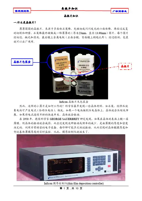
晶振片知识一﹑什么是晶振片?薄薄圆圆的晶振片,来源于多面体石英棒,先被切成闪闪发光的六面体棒,再经过反复的切割和研磨,石英棒最终被做成一堆薄薄的(厚0.23mm ,直径13.98mm )圆片,每个圆片经切边,抛光和清洗,最后镀上金属电极(正面全镀,背面镀上钥匙孔形),经过检测,包装就可以出厂使用。
Inficon 晶振片及包装盒然而,这样的小薄片是如何工作的?科学家最早发现一些晶体材料,如石英,经挤压就象电池可产生电流(俗称压电性),相反,如果一个电池接到压电晶体上,晶体就会压缩或伸展,如果将电流连续不断的快速开关,晶体就会振动。
在1950年,德国科学家GEORGE SAUERBREY 研究发现,如果在晶体的表面上镀一层薄膜,则晶体的振动就会减弱,而且还发现这种振动或频率的减少,是由薄膜的厚度和密度决定的,利用非常精密的电子设备,每秒钟可能多次测试振动,从而实现对晶体镀膜厚度和邻近基体薄膜厚度的实时监控。
从此,膜厚控制仪就诞生了。
Inficon 膜厚控制仪(thin film deposition controller)二﹑膜厚控制仪是如何测试厚度的?一台镀膜设备往往同时配有石英晶体振荡监控法和光学膜厚监控法两套监控系统,两者相互补充以实现薄膜生产过程中工艺参数的准确性和重复性,提高产品的合格率。
原理和精度﹕石英晶体法监控膜厚,主要是利用了石英晶体的两个效应,即压电效应和质量负荷效应。
石英晶体是离子型的晶体,由于结晶点阵的有规则分布,当发生机械变形时,例如拉伸或压缩时能产生电极化现象,称为压电现象。
石英晶体在9.8×10⁴Pa 的压强下,承受压力的两个表面上出现正负电荷,产生约0.5V 的电位差。
压电现象有逆现象,即石英晶体在电场中晶体的大小会发生变化,伸长或缩短,这种现象称为电致伸缩。
石英晶体压电效应的固有频率不仅取决于其几何尺寸,切割类型,而且还取决于芯片的厚度。
当芯片上镀了某种膜层,使芯片的厚度增大,则芯片的固有频率会相应的衰减。
晶振基础知识介绍晶振:即所谓石英晶体谐振器(无源)和石英晶体振荡器(有源)的统称。
无源和有源的区别:无源晶振为crystal(晶体),而有源晶振则叫做oscillator(振荡器)。
无源晶振需要借助于时钟电路才能产生振荡信号,自身无法振荡起来,所以“无源晶振”这个说法并不准确;有源晶振是一个完整的谐振振荡器。
石英晶体振荡器与石英晶体谐振器都是提供稳定电路频率的一种电子器件。
石英晶体振荡器是利用石英晶体的压电效应来起振,而石英晶体谐振器是利用石英晶体和内置IC共同作用来工作的。
振荡器直接应用于电路中,谐振器工作时一般需要提供3.3V电压来维持工作。
振荡器比谐振器多了一个重要技术参数:谐振电阻(RR),谐振器没有电阻要求。
RR的大小直接影响电路的性能,因此这是各商家竞争的一个重要参数。
晶振的原理:压电效应(物理特性):在水晶片上施以机械应力时,,会产生电荷的偏移,即为压电效应。
逆压电效应:相对在水晶片上印加电场会造成水晶片的变形即产生逆压电效应,利用这种特性产生机械振荡,变换成电气信号。
晶振的作用:一、为频率合成电路提供基准时钟,产生原始的时钟频率。
二、为电路产生震荡电流,发出时钟信号晶振的分类:一、按材质封装(1).金属封装-SEAMTYPE (2).陶瓷封装-GLASSTYPE二、贴装方式(1).直插封装-DIP (2).贴片封装-SMD三、按产品类型(1).crystal resonator—晶体谐振器(无源晶体)(2).crystal oscillator—晶体振荡器(有源晶振)---SPXO 普通有源晶体振荡器---VCXO电压控制晶体振荡器---TCXO 温度补偿晶体振荡器---VC-TCXO压控温补晶体振荡器(3).crystal filter—晶体滤波器(4).tuning fork x’tal (khz)-水晶振动子部分 KDS晶振图例:DT-14/DT-26/DT-38 DMX-26S DSX220G DSO321SR/221SR HC-49S/AT-49DSX321G/221 G SM-14J DSV531SV DSX530G/840GDSA/B321SDA晶振的名词术语:SMT :Surface Mount Technology 表面贴装技术SMD :Surface Mount Device 表面贴装元件OSC :Oscillator Crystal 晶体振荡器TCXO :Temperature Compensate X‘tal Oscillator 温度补偿晶体振荡器VC-TCXO :Voltage Controlled, Temperature Compensated Crystal Oscillator 压控温度补偿晶体振动器 VCXO :Voltage Control Oscillator 压控晶体振动器 DST410S/310S/210A DSX320G DSA/B321SCL HC-49SMD/SMD-49晶振的重要参数:1、标称频率F:晶体元件规范(或合同)指定的频率。
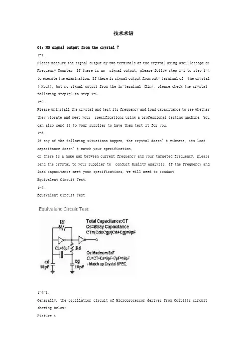
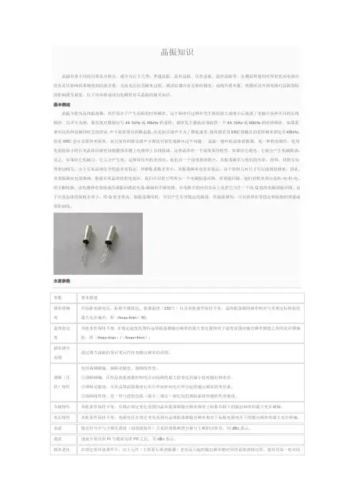
技术术语01:NO signal output from the crystal ?1-1.Please measure the signal output by two terminals of the crystal using Oscilloscope or Frequency Counter. If there is no signal output, please follow step 1-1 to step 1-4 to execute the examination. If there is signal output from out- terminal of the crystal ( Xout), but no signal output from the in-terminal (Xin), please check the crystal following step1-5 to step 1-6.1-2.Please uninstall the crystal and test its frequency and load capacitance to see whether they vibrate and meet your specifications using a professional testing machine. You can also send it to your supplier to have them test it for you.1-3.If any of the following situations happen, the crystal doesn’t vibrate, its load capacitance doesn’t match your specification,or there is a huge gap between current frequency and your targeted frequency, please send the crystal to your supplier to conduct Quality Analysis. If the frequency and load capacitance meet your specifications, we will need to conductEquivalent Circuit Test.1-4.Equivalent Circuit Test1-4-1.Generally, the oscillation circuit of Microprocessor derives from Colpitts circuit showing below:Picture 1Cd and Cg are external load capacitances, which have been built in the chip set. (Please refer to the Specifications of thechip set)Rf is the feedback resistance with200KΩ~1MΩ. It’s built in the chip set generally. Rd is the Limit Resistor with 470Ω~1KΩ. This resistance is not necessary for common circuit but only for circuits havinghigh power supply.1-4-2.A stable oscillation circuit requires a negative resistance and its value should be at least five times of the crystalresistance. It can be written as |-R| > 5 Rr.For example, to acquire a stable oscillation circuit, the value of negative resistance of the IC must be under –200Ω whenthe value of the crystal resistance is 40Ω.1-4-3.“Negative resistance” is the yardstick to evaluate the quality of an oscillation circuit. Under some circumstances such asaging, thermal change, voltage change, and etc., the circuit might not oscillate if the value of “ Q” is low. Thus, it’s veryimportant to measure the negative resistance (-R )following the instructions below:(1) Connect the resistance (R) with the crystal in series(2) Adjust the value of R from the start point to the stop point of the oscillation.(3) Measure the value of R during oscillating.(4) You will be able to obtain the value of negative resistance, |–R| = R + Rr, and Rr = crystal resistance.P.S. the stray capacitance of the connected circuit might affect measured values.1-4-4.If the parameters of the crystal are normal but it’s not working steadily within theoscillation circuit, we will have to findout whether the resistance valu e of the IC is too low to drive the circuit. If that’s the case, we have three methods toimprove such situation:Lower the value of external capacitance(Cd and Cg), and adopt other crystal with lower load capacitance (CL).Adopt a crystal with lower resistance (Rr).Use the design of unequal values of Cd and Cg. We can increase the load capacitance of Cd (Xout) and decrease theload capacitance of Cg(Xin) to raise the output of waveform amplitude from Xin which will be used in its back-endcircuit.1-5.When there is signal output from Xout but not Xin, it represents the case that the power consumption of the rear -electrode Backend Circuit is extremely huge. We can add a buffer between the output of the circuit and its rear electrodeto drive the back-end Circuit.1-6.Except the method of 1-5 mentioned above, you can also follow the three methods in step 1-4-4. Pleasecontact the field application engineers of crystal or IC manufacturers for further assistance, if your problem can’t besolved.02. System is not functioning because of no adequate output waveform amplitude from the crystal ?2-1.Please measure the signals from the two terminals of the crystal using Oscilloscope or Frequency Counter, if the Frequencyis not within the specification and it’s output waveform amplitude is not adequate (for example, over+/- 200ppm), pleasefollow step 2-3 to step 2-5.2-2.The formula for Capacitances versus Frequency is as following:FL = FR * ( 1 + C1 / 2 * ( C0 + CL) ) whereThe curve represents the variation of capacitance changes versus variation of frequency changes ( Frequency pullability):If the frequency measured by Frequency Counter is higher than the targeted frequency, we should increase the value ofcapacitances (CL, or Cd & Cg ) to lower the frequency to the targeted frequency, vice versa.Please check whether the waveform amplitude is improved or not after we adjust the frequency. If it’s improved, thatindicates the case that the original design of the circuit is not tuned to the best resonant point for the crystal. The crystalshould function normally after the resonant point is adjusted.2-3.If the waveform amplitude is not improved even the frequency is pretty much close to the targeted frequency, we canimprove it using three methods below:Method 1: Lower the value of external capacitance (Cd, and Cg) , and adopt crystal with lower loadapacitance (CL).Method 2: Adopt the crystal with lower resistance(Rr).Method 3: Use the design of unequal values of Cd and Cg.We can increase the load capacitance of Cd (Xout) and decrease the load capacitance of Cg(Xin) to raise the output ofwaveform amplitude from Xin which will be used in its back-end Circuit.We suggest that you use above methods to save costs and assure safety2-4.Please use the Frequency Counter to measuring the crystal to ensure that the adjusted frequency still meets originalspecification after the waveform amplitude has been improved. If the frequency doesn’t meet the specification, pleaseadopt a crystal with suitable CL value according to your targeted frequency.2-5.Please adopt a crystal with lower CL if the frequency is much higher than the targeted frequency, vice versa.03. System is not functioning due to high deviation of output frequency ?3-1.We can improve the problem that deviation of frequency output is over the limit by following methods:Adjust the values of external capacitance, Cd & Cg.If the frequency measured by Frequency Counter is higher than targeted frequency, we should increase the externalcapacitance, CL ( or the values of Cd & Cg ), to lower the frequency to our targeted frequency, vice versa.Adopt a crystal with different value of capacitance(CL).Adopt a crystal with lower capacitance if the frequency is much higher than the targeted frequency, vice versa.3-2.Please check whether the waveform amplitude is normal or not using Oscilloscope, after the correct capacitance is adoptedand the frequency is adjusted to target. Under the situation that the waveform amplitude is shrunk due to adding externalcapacitances, please use method 2 to adjust the frequency ( lower external capacitances and adopt a crystal with lowercapacitance).石英晶体基础理论•石英晶体特性石英是一种压电材料,被发觉是自然界所产生的透明结晶物,它所展现的是非常稳定的压电效应,从化学与机械上的特性在早期的电子实验引起了极大的关注。
晶振重要基础知识点晶振(Crystal Oscillator)是一种电子元件,作为电路中的重要组成部分,主要用于产生稳定的电信号。
在电子技术领域中,晶振是一项重要的基础知识点,对于电路的设计和工作原理具有关键性的影响。
以下是有关晶振的几个重要基础知识点。
1. 晶体的特性:晶振的核心部件是晶体,通常采用石英晶体。
晶体具有特殊的物理特性,能够产生稳定的振荡频率。
这是由于晶体的晶格结构和内部电荷特性决定的。
因此,晶体的选择对于晶振的性能和稳定性至关重要。
2. 振荡电路的构成:晶振一般包含振荡电路,该电路由晶体振荡器、放大电路和输出电路组成。
晶体振荡器是整个晶振的核心部件,用于产生基准频率信号。
放大电路用于放大振荡器输出的信号,以便提供足够的幅度和驱动能力。
输出电路则将放大后的信号输出给其他电路或系统。
3. 振荡频率和精度:晶振的一个关键参数是振荡频率,即晶体的振荡周期。
该频率取决于晶体的物理特性和电路参数。
晶振的精度取决于晶体的制作工艺和电路设计。
通常情况下,晶振的频率精度可以达到百万分之一甚至更高的水平。
4. 温度特性:晶振的频率通常会随着温度的变化而发生微小的变化,这是由晶体的温度特性决定的。
为了确保晶振在不同温度下的稳定性,通常会采取一些温度补偿措施,例如使用温度补偿电路或选择温度稳定性较好的晶体材料。
5. 应用领域:晶振在电子领域有广泛的应用。
最常见的应用是在时钟电路中,用于提供计时信号。
此外,晶振还用于无线通信设备、计算机系统、自动化控制系统等领域,为这些系统提供稳定的基准时钟信号。
综上所述,晶振作为电子领域的重要基础知识点,涉及晶体的特性、振荡电路的构成、振荡频率和精度、温度特性以及应用领域等方面。
深入理解和熟悉晶振的相关知识,对于电子工程师和电路设计师来说至关重要,能够帮助他们设计出稳定性高、性能优越的电子系统。
晶振知识介绍
1晶振在线路中的符号是"X”,"Y”
2晶振的名词解释:能产生具有一定幅度及频率波形的振荡器.
3晶振在线路图中的表示符号:
4晶振的测量方法:
测量电阻方法:用万用表RX10K档测量石英晶体振荡器的正,反向电阻值.正常时应为无穷大.若测得石英晶体振荡器有一定的阻值或为零,则说明该石英晶体振荡器已漏电或击穿损坏.
动态测量方法:用是波器在电路工作时测量它的实际振荡频是否符合该晶体的额定振荡频率,如果是,说明该晶振是正常的,如果该晶体的额定振荡频率偏低,偏高或根本不起振,表明该晶振已漏电或击穿损坏。
晶振mhz晶振MHz是指晶体振荡器的频率单位,其意义在于帮助电子设备精准计时,达到更高的稳定性和精度。
如何选择和使用晶振MHz,是电子设备开发者必须掌握的重要知识。
一、什么是晶振晶振是一种集成电路,用来产生基准频率的方波信号。
它由一块晶片和两个引脚组成,一端连接电路器件,另一端连接外部电源。
晶振的基本原理是通过晶片的正反面接上压电陶瓷晶片,当外加直流电源后,晶片受到电磁力的作用使得晶片开始振荡。
输出的信号可以通过校准和滤波后接入某些电子设备中。
二、晶振MHz的作用晶振MHz的作用在电子设备中类似于机械表中的发条,能够产生精准的基准频率输入,从而支持设备的运转、同步和计量功能。
不同种类的晶振MHz有不同的工作范围和精度要求,下面是一些常见的晶振MHz值及其使用范围:1. 4MHz, 8MHz, 12MHz, 16MHz:用于单片机控制电路、据点VGA 信号输入,常见的ARM、AVR、51系单片机.2. 20MHz, 24MHz, 25MHz: 用于USB、ETH、SATA及高速ADC等低功耗电路,常见的STM32系列单片机。
3. 32.768kHz:用于计时计量电路,如时钟,石英表,定时开关等。
三、晶振MHz的选择晶振MHz的选择需要考虑贴片(SMD)或者插针(DIP)的形态、工作环境的温度和湿度、需要的频率值和精度要求等因素。
1.形态选择:如果计划使用超小型电子设备,则需要选择体积小巧且便于贴片的SMD形态结构。
如果需要进行调整和更换,则需要选择带有引脚的DIP形态。
2.温湿度要求:如果电子设备需要在高温或者潮湿的环境中工作,需要选择有防潮和抗高温能力的晶振MHz。
如果在低温或者高海拔领域使用,需要有较高的稳定性和精度。
3.要求精度:一些需要计量精确时间或频率的应用,比如雷达的刹车和跟踪之间的计时、计算机内部总线时钟、数字电路等,则可选择精度较高的晶振MHz。
而像转换低频信号的晶振MHz则不需要那么高的精度。
晶振知识晶振有着不同使用要求及特点,通分为以下几类:普通晶振、温补晶振、压控晶振、温控晶振等。
在测试和使用时所供直流电源应没有足以影响其准确度的纹波含量,交流电压应无瞬变过程。
测试仪器应有足够的精度,连线合理布置,将测试及外围电路对晶振指标的影响降至最低。
以下内容将逐项为您解答有关晶振的相关知识。
基本概述晶振全称为晶体振荡器,其作用在于产生原始的时钟频率,这个频率经过频率发生器的放大或缩小后就成了电脑中各种不同的总线频率。
以声卡为例,要实现对模拟信号44.1kHz或48kHz的采样,频率发生器就必须提供一个44.1kHz或48kHz的时钟频率。
如果需要对这两种音频同时支持的话,声卡就需要有两颗晶振。
但是娱乐级声卡为了降低成本,通常都采用SRC将输出的采样频率固定在48kHz,但是SRC会对音质带来损害,而且现在的娱乐级声卡都没有很好地解决这个问题。
晶振一般叫做晶体谐振器,是一种机电器件,是用电损耗很小的石英晶体经精密切割磨削并镀上电极焊上引线做成。
这种晶体有一个很重要的特性,如果给它通电,它就会产生机械振荡,反之,如果给它机械力,它又会产生电,这种特性叫机电效应。
他们有一个很重要的特点,其振荡频率与他们的形状,材料,切割方向等密切相关。
由于石英晶体化学性能非常稳定,热膨胀系数非常小,其振荡频率也非常稳定,由于控制几何尺寸可以做到很精密,因此,其谐振频率也很准确。
根据石英晶体的机电效应,我们可以把它等效为一个电磁振荡回路,即谐振回路。
他们的机电效应是机-电-机-电..的不断转换,由电感和电容组成的谐振回路是电场-磁场的不断转换。
在电路中的应用实际上是把它当作一个高Q值的电磁谐振回路。
由于石英晶体的损耗非常小,即Q值非常高,做振荡器用时,可以产生非常稳定的振荡,作滤波器用,可以获得非常稳定和陡削的带通或带阻曲线。
主要参数晶体振荡器也分为无源晶振和有源晶振两种类型。
无源晶振与有源晶振(谐振)的英文名称不同,无源晶振为crystal(晶体),而有源晶振则叫做oscillator(振荡器)。
无源晶振无源晶振与与有源晶振无源晶振无源晶振((Crystal :):内只有一片按一定轴向切割的石英晶体薄片内只有一片按一定轴向切割的石英晶体薄片内只有一片按一定轴向切割的石英晶体薄片,,供接入运放供接入运放((或微处理器的Xtal 端)以形成振荡以形成振荡。
((依靠配合其他依靠配合其他IC 内部振荡电路工作内部振荡电路工作))有源晶振有源晶振((Oscillator )::内带运放内带运放内带运放,,工作在最佳状态工作在最佳状态,,送入电源后送入电源后,,可直接输出一定频率的等可直接输出一定频率的等幅幅正弦波(。
(晶振晶振+振动电路振动电路,,封装在一起封装在一起,,加上电源加上电源,,就有波形输出就有波形输出))※无源晶振是有2个引脚的无极性元件,需要借助于时钟电路才能产生振荡信号,自身无法振荡起来无源晶振需要用微处理器片内的振荡器,在datasheet 上有建议的连接方法。
无源晶振没有电压的问题,信号电平是可变的,也就是说是根据起振电路来决定的,同样的晶振可以适用于多种电压,可用于多种不同时钟信号电压要求的微处理器,而且价格通常也较低,因此对于一般的应用如果条件许可建议用晶体,这尤其适合于产品线丰富批量大的生产者。
无源晶振相对于晶振而言其缺陷是信号质量较差,通常需要精确匹配外围电路(用于信号匹配的电容、电感、电阻等),更换不同频率的晶体时周边配置电路需要做相应的调整。
使用时建议采用精度较高的石英晶体,尽可能不要采用精度低的陶瓷晶体。
※有源晶振有4只引脚,是一个完整的振荡器,里面除了石英晶体外,还有晶体管和阻容元件 。
有源晶振不需要微处理器的内部振荡器,信号质量好,比较稳定,而且连接方式相对简单(主要是做好电源滤波,通常使用一个电容和电感构成的PI 型滤波网络,输出端用一个小阻值的电阻过滤信号即可),不需要复杂的配置电路。
相对于无源晶体,有源晶振的缺陷是其信号电平是固定的,需要选择好合适输出电平,灵活性较差,价格相对较高。
关于晶振的一些知识2010-10-22 08:42:19| 分类:资料 | 标签:晶振|举报|字号订阅有源晶振有很多种供电电压的,2.5V 2.8V 3V 3.3V 5V 9V 12V 等3.3V晶振用在5V电路上有可能会烧坏晶振,晶振如果是5V供电,根据设计有的是可以使用3.3V供电,有的不可以另外一般3.3V供电的晶振有一个电压允许范围,比如3.3V供电的晶振,3V供电也是可以使用的,但不能低到2.8V,这些都是根据晶振特性来确定的,高端晶振最好是在使用的时候电压与要求电压相符合我发现在使用晶振时会和它并一个电阻,一般1M以上,我把它去掉,板子仍可正常工作,请问这个电阻有什么用?可以不用吗?这个电阻是反馈电阻,是为了保证反相器输入端的工作点电压在VDD/2 ,这样在振荡信号反馈在输入端时,能保证反相器工作在适当的工作区。
虽然你去掉该电阻时,振荡电路仍工作了。
但是如果从示波器看振荡波形就会不一致了,而且可能会造成振荡电路工作点不合适而停振。
所以千万不要省略此电阻。
今天更换陶瓷晶振,但是不起振,经过测试,将晶振并联一个1M电阻,晶振能够正常起振。
原因:这个电阻是为了使本来为逻辑反相器的器件工作在线性区, 以获得增益, 在饱和区是没有增益的,而没有增益是无法振荡的. 如果用芯片中的反相器来作振荡, 必须外接这个电阻, 对于CMOS而言可以是1M以上, 对于TTL则比较复杂, 视不同类型(S,LS...)而定. 如果是芯片指定的晶振引脚, 如在某些微处理器中, 常常可以不加, 为芯片内部已经制作了, 要仔细阅读DATA SHEET的有关说明.附:电阻的作用是将电路内部的反向器加一个反馈回路,形成放大器,当晶体并在其中会使反馈回路的交流等效按照晶体频率谐振,由于晶体的Q值非常,因此电阻在很大的范围变化都不会影响输出频率。
过去,曾经试验此电路的稳定性时,试过从100K ~20M都可以正常启振,但会影响脉宽比的。
晶振术语解释1、晶振:即所谓石英晶体谐振器和石英晶体时钟振荡器的统称。
不过由于在消费类电子产品中,谐振器用的更多,所以一般的概念中把晶振就等同于谐振器理解了。
后者就是通常所指钟振。
2、分类。
首先说一下谐振器。
谐振器一般分为插件(Dip)和贴片(SMD)。
插件中又分为HC-49U、HC-49U/S、音叉型(圆柱)。
HC-49U一般称49U,有些采购俗称“高型”,而HC-49U/S一般称49S,俗称“矮型”。
音叉型按照体积分可分为3*8,2*6,1*5,1*4等等。
贴片型是按大小和脚位来分类。
例如7*5(0705)、6*3.5(0603),5*3.2(5032)等等。
脚位有4pin和2pin之分。
而振荡器也是可以分为插件和贴片。
插件的可以按大小和脚位来分。
例如所谓全尺寸的,又称长方形或者14pin,半尺寸的又称为正方形或者8pin。
不过要注意的是,这里的14pin和8pin都是指振荡器内部核心IC的脚位数,振荡器本身是4pin。
而从不同的应用层面来分,又可分为OSC(普通钟振),TCXO(温度补偿),VCXO(压控),OCXO(恒温)等等。
3、基本术语。
我想这也是很多采购同学比较模糊的地方。
这里我选了一些常用的谐振器术语拿来做一下解释。
Frequency Tolerance(调整频差):在规定条件下,在基准温度(25±2℃)与标称频率允许的偏差。
一般用PPm(百万分之)表示。
Frequency Stability(温度频差):指在规定的工作温度范围内,与标称频率允许的偏差。
用PPm 表示。
Aging(年老化率):在规定条件下,晶体工作频率随时间而允许的相对变化。
以年为时间单位衡量时称为年老化率。
Shunt Capacitance(静电容):等效电路中与串联臂并接的电容,也叫并电容,通常用C0表示。
Load Capacitance(负载电容):与晶体一起决定负载谐振频率fL的有效外界电容,通常用CL表示。
一、什么是晶振?晶振是石英振荡器的简称,英文名为Crystal,它是时钟电路中最重要的部件,它的主要作用是向显卡、网卡、主板等配件的各部分提供基准频率,它就像个标尺,工作频率不稳定会造成相关设备工作频率不稳定,自然容易出现问题。
晶振还有个作用是在电路产生震荡电流,发出时钟信号.晶振是晶体振荡器的简称。
它用一种能把电能和机械能相互转化的晶体在共振的状态下工作,以提供稳定,精确的单频振荡。
在通常工作条件下,普通的晶振频率绝对精度可达百万分之五十。
高级的精度更高。
有些晶振还可以由外加电压在一定范围内调整频率,称为压控振荡器(VCO)。
晶振在数字电路的基本作用是提供一个时序控制的标准时刻。
数字电路的工作是根据电路设计,在某个时刻专门完成特定的任务,如果没有一个时序控制的标准时刻,整个数字电路就会成为“聋子”,不知道什么时刻该做什么事情了。
晶振的作用是为系统提供基本的时钟信号。
通常一个系统共用一个晶振,便于各部分保持同步。
有些通讯系统的基频和射频使用不同的晶振,而通过电子调整频率的方法保持同步。
晶振通常与锁相环电路配合使用,以提供系统所需的时钟频率。
如果不同子系统需要不同频率的时钟信号,可以用与同一个晶振相连的不同锁相环来提供。
电路中,为了得到交流信号,可以用RC、LC谐振电路取得,但这些电路的振荡频率并不稳定。
在要求得到高稳定频率的电路中,必须使用石英晶体振荡电路。
石英晶体具有高品质因数,振荡电路采用了恒温、稳压等方式以后,振荡频率稳定度可以达到10^(-9)至10^(-11)。
广泛应用在通讯、时钟、手表、计算机……需要高稳定信号的场合。
石英晶振不分正负极, 外壳是地线,其两条不分正负二、晶振的使用晶振(石英晶体),在电气上它可以等效成一个电容和一个电阻并联再串联一个电容的二端网络,电工学上这个网络有两个谐振点,以频率的高低分其中较低的频率是串联谐振,较高的频率是并联谐振。
由于晶体自身的特性致使这两个频率的距离相当的接近,在这个极窄的频率范围内,晶振等效为一个电感,所以只要晶振的两端并联上合适的电容它就会组成并联谐振电路。
晶振的一般知识和质量控制[2008-12-8 11:00:37]晶振的一般知识和质量控制1. 晶振的作用是产生时钟信号,晶体谐振器与其它器件共同组成晶体振荡器。
2.晶体谐振器,要达到稳定性好,要求串联谐振电阻既要小又要一致性好,同时激励功率变化带来的阻抗变量越小,晶体的谐振点容易一致,这样外围电路调试比较容易,使产品更稳定,那么具体如何实现呢?第一,用Q值(Q值是等效电路中动态臂谐振时的品质因数,振荡电路所能获得的最大稳定性直接与电路中晶体的Q值相关。
Q值越高,晶体带宽越小,电抗值变化越陡,外部电抗对晶体影响越小)高的水晶材料,能降低串联电阻,同时控制胶量的匀称性;第二,要求生产车间净化程度很高,能减少本体之外的灰尘附着物带来的干扰,降低阻抗变量;第三,成品测试将并联谐振电阻和DLD值(功率改变引起的阻抗变量)控制在相对更小的范围内。
3.根据经验及晶体本身的特性总结出:第一,在使用过程中,外围匹配电容(包括杂散电容)愈接近晶体标称电容,电路形成的振荡频率愈接近标称频率。
电路的稳定性由晶体本身和外围电路共同决定,最佳电路应让工作频率高与标准频率8PPM左右,因为频率每年都要下降3PPM左右即年老化率,这样才能保证电路中振荡频率在5年内准确度很高;第二,晶体在使用中还要具有一定的温度稳定性和抗震性及可焊性,如何实现?1)提高晶片加工精度,降低晶体封闭壳中氮气的露点,通过高低温测试试验;2)生产上,用优质胶,点匀和及时烤胶,检查剔除有崩边的晶片,通过跌落和机械振动测试(100-20000G)试验,提高包装保护;3)同时增加240±10℃和5S条件下的耐高温测试。
4.晶体振荡器分直插(DIP-14,DIP-8)和SMD贴片。
直插式的一般为非三态线路,有需求可选三态规格,SMD 式的为三态线路输出。
在使用中DIP系列1#角在无特殊说明时为断开的,静电对DIP破坏性较小。
SMD系列1#角内部相连,外接时需断开,静电对其破坏最大,容易击穿IC,须作静电保护;另外,SMD系列晶振在焊接过程中不要温度过高,时间过长,一般控制在260℃±5℃,少于5秒。
晶振的定义: 晶振的英文名称为crystal. 石英晶体经精密切割磨削并镀上电极焊上引线做成,主要是为电路提供频率基准的元器件。
晶振的分类:1.按制作材料,分为石英晶振和陶瓷晶振。
低,陶瓷,而有工作,精度比晶振要低,但它不需要电源供电,有起振电路即可起振,一般有两个引脚,价格较低。
有源晶振内部含有石英晶体和匹配电容等外围电路,精度高、输出信号稳定,不需要设计外围电路、使用方便,但需要电源供电,有源晶振一般是四管脚封状,有电源、地线、振荡输出和一个空置端。
使用有源晶振时要特别注意,电源必须是稳压的且电源引线尽量短,并尽量与系统中使用晶振信号的芯片共地。
3、从封装形式上分有直插型(DIP)和贴片型(SMD)。
4、按谐振频率精度,分为高精度型、中精度型和普通型晶振。
5、按应用特性,分为串联谐振型晶振和并联谐振型晶振。
,是成正比。
这种现象就称“正压电效应”。
反之,在电场作用下,晶体产生形变,其形变大小与电场强度成正比,这种现象称“逆压电效应”。
利用压电效应,当极板外加交变电压时,产生机械形变;机械形变反过来产生交变电场。
机械形变振幅较小,晶体振动的频率比较稳定。
当外加交变电压的频率和晶体的固有频率相等时,机械振动的振幅急剧增加。
石英晶片的切型:在制造工艺中,首先要对石英晶体原材料进行切割研磨处理,其中一道很重要的工序是定角。
由于石英片的取向不同,其压电特性、弹性特性和强度特性就不同,用它来制造的谐振器的性能也不一样,经过大量研究,已发现了几十种有用的切割方式。
切型的习惯表示方法:AT, BT,CT,DT,ET,FC, SC,LC等。
石英晶体的振动模式:石英晶体常规技术指标:1/106)ppm晶体元件在串联谐振频率Fr时的电阻值。
•负载电容(CL )CL≈(C1C2/(C1+C2))+C杂散与晶体元件一起决定负载谐振频率FL的有效外界电容。
这里C杂散指晶体元件周边电路的分布电容。
资料介绍PCB电路板的分布电容多为5-6pF 。