MT7968规格书-中文_Rev1.40
- 格式:pdf
- 大小:519.52 KB
- 文档页数:8


PRECHARGE OperationInput A10 determines whether one bank or all banks are to be precharged and, in thecase where only one bank is to be precharged, inputs BA[2:0] select the bank.When all banks are to be precharged, inputs BA[2:0] are treated as “Don’t Care.” After abank is precharged, it is in the idle state and must be activated prior to any READ orWRITE commands being issued.SELF REFRESH OperationThe SELF REFRESH operation is initiated like a REFRESH command except CKE is LOW.The DLL is automatically disabled upon entering SELF REFRESH and is automaticallyenabled and reset upon exiting SELF REFRESH.All power supply inputs (including V REFCA and V REFDQ) must be maintained at valid lev-els upon entry/exit and during self refresh mode operation. V REFDQ may float or notdrive V DDQ/2 while in self refresh mode under certain conditions:•V SS < V REFDQ < V DD is maintained.•V REFDQ is valid and stable prior to CKE going back HIGH.•The first WRITE operation may not occur earlier than 512 clocks after V REFDQ is valid.•All other self refresh mode exit timing requirements are met.The DRAM must be idle with all banks in the precharge state (t RP is satisfied and nobursts are in progress) before a self refresh entry command can be issued. ODT mustalso be turned off before self refresh entry by registering the ODT ball LOW prior to theself refresh entry command (see On-Die Termination (ODT) ( for timing requirements).If R TT,nom and R TT(WR) are disabled in the mode registers, ODT can be a “Don’t Care.”After the self refresh entry command is registered, CKE must be held LOW to keep theDRAM in self refresh mode.After the DRAM has entered self refresh mode, all external control signals, except CKEand RESET#, are “Don’t Care.” The DRAM initiates a minimum of one REFRESH com-mand internally within the t CKE period when it enters self refresh mode.The requirements for entering and exiting self refresh mode depend on the state of theclock during self refresh mode. First and foremost, the clock must be stable (meetingt CK specifications) when self refresh mode is entered. If the clock remains stable andthe frequency is not altered while in self refresh mode, then the DRAM is allowed to exitself refresh mode after t CKESR is satisfied (CKE is allowed to transition HIGH t CKESRlater than when CKE was registered LOW). Since the clock remains stable in self refreshmode (no frequency change), t CKSRE and t CKSRX are not required. However, if theclock is altered during self refresh mode (if it is turned-off or its frequency changes),then t CKSRE and t CKSRX must be satisfied. When entering self refresh mode, t CKSREmust be satisfied prior to altering the clock's frequency. Prior to exiting self refreshmode, t CKSRX must be satisfied prior to registering CKE HIGH.When CKE is HIGH during self refresh exit, NOP or DES must be issued for t XS time. t XSis required for the completion of any internal refresh already in progress and must besatisfied before a valid command not requiring a locked DLL can be issued to the de-vice. t XS is also the earliest time self refresh re-entry may occur. Before a command re-quiring a locked DLL can be applied, a ZQCL command must be issued, t ZQOPER tim-ing must be met, and t XSDLL must be satisfied. ODT must be off during t XSDLL.Figure 93: Self Refresh Entry/Exit TimingCKCK#CommandAddressCKEODT 2RESET#2Exit self refresh mode (asynchronous)Don’t CareIndicates breakin time scale Notes: 1.The clock must be valid and stable, meeting t CK specifications at least t CKSRE after en-tering self refresh mode, and at least t CKSRX prior to exiting self refresh mode, if the clock is stopped or altered between states Ta0 and Tb0. If the clock remains valid and unchanged from entry and during self refresh mode, then t CKSRE and t CKSRX do not apply; however, t CKESR must be satisfied prior to exiting at SRX.2.ODT must be disabled and R TT off prior to entering self refresh at state T1. If both R TT,nom and R TT(WR) are disabled in the mode registers, ODT can be a “Don’t Care.”3.Self refresh entry (SRE) is synchronous via a REFRESH command with CKE LOW.4. A NOP or DES command is required at T2 after the SRE command is issued prior to the inputs becoming “Don’t Care.”5.NOP or DES commands are required prior to exiting self refresh mode until state Te0.6.t XS is required before any commands not requiring a locked DLL.7.t XSDLL is required before any commands requiring a locked DLL.8.The device must be in the all banks idle state prior to entering self refresh mode. For example, all banks must be precharged, t RP must be met, and no data bursts can be in progress.9.Self refresh exit is asynchronous; however, t XS and t XSDLL timings start at the first rising clock edge where CKE HIGH satisfies t ISXR at Tc1. t CKSRX timing is also measured so that t ISXR is satisfied at Tc1.Extended Temperature UsageMicron’s DDR3 SDRAM support the optional extended case temperature (T C) range of0°C to 95°C. Thus, the SRT and ASR options must be used at a minimum.The extended temperature range DRAM must be refreshed externally at 2x (double re-fresh) anytime the case temperature is above 85°C (and does not exceed 95°C). The ex-ternal refresh requirement is accomplished by reducing the refresh period from 64ms to32ms. However, self refresh mode requires either ASR or SRT to support the extendedtemperature. Thus, either ASR or SRT must be enabled when T C is above 85°C or selfrefresh cannot be used until T C is at or below 85°C. Table 75 summarizes the two exten-ded temperature options and Table 76 summarizes how the two extended temperatureoptions relate to one another.Table 75: Self Refresh Temperature and Auto Self Refresh DescriptionTable 76: Self Refresh Mode SummaryPower-Down ModePower-down is synchronously entered when CKE is registered LOW coincident with aNOP or DES command. CKE is not allowed to go LOW while an MRS, MPR, ZQCAL,READ, or WRITE operation is in progress. CKE is allowed to go LOW while any of theother legal operations (such as ROW ACTIVATION, PRECHARGE, auto precharge, or RE-FRESH) are in progress. However, the power-down I DD specifications are not applicableuntil such operations have completed. Depending on the previous DRAM state and thecommand issued prior to CKE going LOW, certain timing constraints must be satisfied(as noted in Table 77). Timing diagrams detailing the different power-down mode entryand exits are shown in Figure 94 (page 176) through Figure 103 (page 180).Table 77: Command to Power-Down Entry ParametersNote: 1.If slow-exit mode precharge power-down is enabled and entered, ODT becomes asyn-chronous t ANPD prior to CKE going LOW and remains asynchronous until t ANPD +t XPDLL after CKE goes HIGH.Entering power-down disables the input and output buffers, excluding CK, CK#, ODT,CKE, and RESET#. NOP or DES commands are required until t CPDED has been satis-fied, at which time all specified input/output buffers are disabled. The DLL should be ina locked state when power-down is entered for the fastest power-down exit timing. Ifthe DLL is not locked during power-down entry, the DLL must be reset after exitingpower-down mode for proper READ operation as well as synchronous ODT operation.During power-down entry, if any bank remains open after all in-progress commands arecomplete, the DRAM will be in active power-down mode. If all banks are closed after allin-progress commands are complete, the DRAM will be in precharge power-downmode. Precharge power-down mode must be programmed to exit with either a slow exitmode or a fast exit mode. When entering precharge power-down mode, the DLL isturned off in slow exit mode or kept on in fast exit mode.The DLL also remains on when entering active power-down. ODT has special timingconstraints when slow exit mode precharge power-down is enabled and entered. Referto Asynchronous ODT Mode (page 197) for detailed ODT usage requirements in slowexit mode precharge power-down. A summary of the two power-down modes is listed inTable 78 (page 175).While in either power-down state, CKE is held LOW, RESET# is held HIGH, and a stableclock signal must be maintained. ODT must be in a valid state but all other input signalsare “Don’t Care.” If RESET# goes LOW during power-down, the DRAM will switch out ofpower-down mode and go into the reset state. After CKE is registered LOW, CKE mustremain LOW until t PD (MIN) has been satisfied. The maximum time allowed for power-down duration is t PD (MAX) (9 × t REFI).The power-down states are synchronously exited when CKE is registered HIGH (with arequired NOP or DES command). CKE must be maintained HIGH until t CKE has beensatisfied. A valid, executable command may be applied after power-down exit latency,t XP, and t XPDLL have been satisfied. A summary of the power-down modes is listed be-low.For specific CKE-intensive operations, such as repeating a power-down-exit-to-refresh-to-power-down-entry sequence, the number of clock cycles between power-down exitand power-down entry may not be sufficient to keep the DLL properly updated. In addi-tion to meeting t PD when the REFRESH command is used between power-down exitand power-down entry, two other conditions must be met. First, t XP must be satisfiedbefore issuing the REFRESH command. Second, t XPDLL must be satisfied before thenext power-down may be entered. An example is shown in Figure 104 (page 181).Table 78: Power-Down Modes。
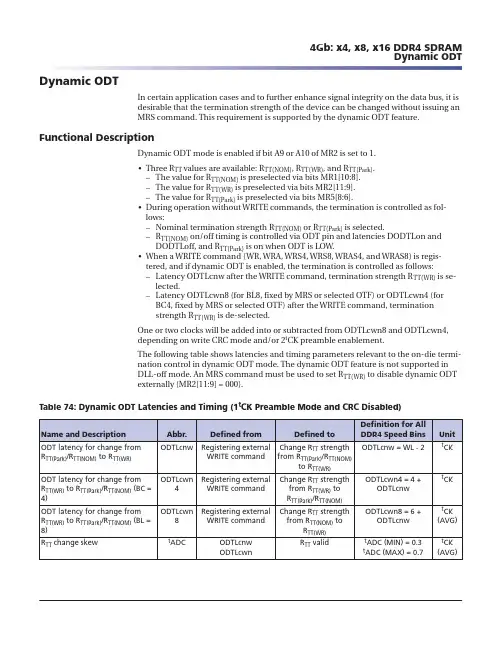
Dynamic ODTIn certain application cases and to further enhance signal integrity on the data bus, it isdesirable that the termination strength of the device can be changed without issuing anMRS command. This requirement is supported by the dynamic ODT feature.Functional DescriptionDynamic ODT mode is enabled if bit A9 or A10 of MR2 is set to 1.•Three R TT values are available: R TT(NOM), R TT(WR), and R TT(Park).–The value for R TT(NOM) is preselected via bits MR1[10:8].–The value for R TT(WR) is preselected via bits MR2[11:9].–The value for R TT(Park) is preselected via bits MR5[8:6].•During operation without WRITE commands, the termination is controlled as fol-lows:–Nominal termination strength R TT(NOM) or R TT(Park) is selected.–R TT(NOM) on/off timing is controlled via ODT pin and latencies DODTLon andDODTLoff, and R TT(Park) is on when ODT is LOW.•When a WRITE command (WR, WRA, WRS4, WRS8, WRAS4, and WRAS8) is regis-tered, and if dynamic ODT is enabled, the termination is controlled as follows:–Latency ODTLcnw after the WRITE command, termination strength R TT(WR) is se-lected.–Latency ODTLcwn8 (for BL8, fixed by MRS or selected OTF) or ODTLcwn4 (forBC4, fixed by MRS or selected OTF) after the WRITE command, terminationstrength R TT(WR) is de-selected.One or two clocks will be added into or subtracted from ODTLcwn8 and ODTLcwn4,depending on write CRC mode and/or 2t CK preamble enablement.The following table shows latencies and timing parameters relevant to the on-die termi-nation control in dynamic ODT mode. The dynamic ODT feature is not supported inDLL-off mode. An MRS command must be used to set R TT(WR) to disable dynamic ODTexternally (MR2[11:9] = 000).Table 74: Dynamic ODT Latencies and Timing (1t CK Preamble Mode and CRC Disabled)4Gb: x4, x8, x16 DDR4 SDRAM Dynamic ODTFigure 161: READ (BC4: Fixed) to WRITE (BC4: Fixed) with 1t CK Preamble and Write CRC in Same or Different Bank GroupCommand DQ x4,BC = 4 (Fixed)CK_t CK_cDQS_t,DQS_cBank GroupAddress AddressDQ x8/X16,BC = 4 (Fixed)Notes: 1.BC = 4 (Fixed), RL = 11 (CL = 11, AL = 0), READ preamble = 1t CK, WL = 9 (CWL = 9, AL =0), WRITE preamble = 1t CK.2.DO n = data-out from column n , DI b = data-in from column b .3.DES commands are shown for ease of illustration; other commands may be valid atthese times.4.BC4 setting activated by MR0[1:0] = 10.5.CA parity = Disable, CS to CA latency = Disable, Read DBI = Disable, Write DBI = Disable,Write CRC = Enable.READ Operation with Command/Address Latency (CAL) EnabledFigure 162: Consecutive READ (BL8) with CAL (3t CK) and 1t CK Preamble in Different Bank GroupCommandw/o CS_nDQCK_tCK_cDQS_t,DQS_cBank GroupAddress Address CS_n Notes: 1.BL = 8, RL = 11 (CL = 11, AL = 0), READ preamble = 1t CK.4Gb: x4, x8, x16 DDR4 SDRAM READ Operation。
HK NATER TECH LIMITEDMT7688核心模块Specification Customer:Description:LH7688EVB-MCustomer P/N:______________________________________ Date:Customer: Provider:HK NATER TECH LIMITEDAdd: Add: 2F,NO.27,2 Baomin Rd.,Baoan Dist.SZ City,China Tel: Tel:0086-755-61522172/135****0050Fax: Fax:0086-755-61522171Attn: Attn:LingoE-mail: E-mail:***************基于MT7688A的Wi-Fi路由模块文档版本:Rev 0.4版本历史:版本日期说明作者备注0.1 2014-Sep-18 初次紧急发布。
T om0.2 2014-Sep-19 增加电气特性部分。
T om0.3 2014-Sep-25 增加SD卡典型电路T om0.4 2014-Oct-09 增加RF典型特性T om1. 模块简介LH-7688-M是一款通用2.4G Wi-Fi路由模块,配合一个Ethernet接口,一个USB口,若干GPIO,它可以适用于很多场合。
比如有线转无线,3G/4G转WiFi,,硬AP,便携式路由器,无线音箱,无线存储等等。
模块大小为56mm*39mm,采用邮票接口(半孔工艺)与母板连接。
WiFi可以使用板载的片状天线,简化客户的整机装配;或者使用I-PEX引出。
模块基于台湾MTK的MT7688A方案,主要特点如下:◆ 无线+有线路由器方案◆ 无线支持802.11b/g/n,最高速率150Mbps◆ 有线支持1WAN或1LAN,10M/100M自适应◆ 适中的RF功率消耗◆ 支持64MB/128MB/256MB DDR2 memory◆ 480Mbps的高速USB接口◆ 3路UART(推荐UART0专用于系统Debug)◆ I2S数字音频接口◆ I2C通信接口◆ 4位/8位SD卡存储接口◆ 丰富的GPIO2. 信 号Pin说明3 @I2S_DO 输出 I2S 数据输出 内部下拉4 I2S_WS 输出 I2S 左右声道对齐5 I2S_CLK输出 I2S 位时钟 6 I2C_SCLK 双向 I2C 时钟线 7 I2C_SD 双向 I2C 数据线 8 SPI_MISO 输入 SPI 主入从出9 *SPI_CS0 输出 SPI 片选0,应悬空 仅供调试10 @SPI_CS1 输出 SPI 片选1 内部下拉,与Flash 型号/容量有关 11 GND地12 @SPI_CLK 输出 SPI 时钟 内部上拉 13 @SPI_MOSI 输出 SPI 主出从入 内部下拉 14 GPIO_0 双向 GPIO_015 @UART_TXD0 输出 UART0发送线 Debug,内部下拉 16 UART_RXD0 输入 UART0接收线 Debug 17 RXIP0 模拟 Ethernet 接收线正 18 RXIN0 模拟 Ethernet 接收线负 19 TXOP0 模拟 Ethernet 发送线正 20 TXON0模拟 Ethernet 发送线负 21 PWM_CH0/SPIS_CS 双向 PWM 通道0/从SPI 片选 22 PWM_CH1/SPIS_CLK 双向 PWM 通道1/从SPI 时钟 23 UART_TXD2/SPIS_MISO 双向 UART2发送线/从SPI 主入从出 24 UART_RXD2/SPIS_MOSI 双向 UART2接收线/从SPI 主出从入 25 GND地26 SD_D7/GPIO18 双向 SD Data7/GPIO18 27 SD_D6/GPIO19 双向 SD Data6/GPIO19 28 SD_D5/GPIO20 双向 SD Data5/GPIO20 29 SD_D4/GPIO21 双向 SD Data4/GPIO21 30 SD_WP_N 输入 SD 写保护检测 31 SD_CD_N 输入 SD 插入检测 引脚 名称 方向 描述备注1 GND地2 I2S_DI 输入 I2S 数据输入33 SD_D0 双向 SD Data034 SD_CLK 输出 SD时钟线35 SD_CMD 双向 SD命令线36 SD_D1 双向 SD Data137 SD_D0 双向 SD Data038 GND 地39 USB_DP 双向 USB 2.0 D+40 USB_DM 双向 USB 2.0 D-41 GND 地42 VIN 电源 3.3V-5.3V直流输入43 VIN 电源 同上44 GND 地45 GND 地46 VOUT 电源 3.3V电源输出47 VOUT 电源 3.3V电源输出48 @PERST_N 输出 GPO 内部上拉49 REF_CLKO 输出 系统时钟输出/GPIO50 WDT_RST_N 双向 WatchDog复位/GPIO 默认恢复出厂设置51 CPURST_N 双向 MT7688A Reset信号 内部RC52 JTRST_N/LINK4 双向 GPIO53 JTCLK/LINK3 双向 GPIO54 JTMS/LINK2 双向 GPIO55 JTDI/LINK1 双向 GPIO56 JTDO/LINK0 输出 GPIO 推荐Ethernet指示57 WLED_N 输出 Wi-Fi状态指示58 @UART_TXD1 输出 UART1发送线 内部上拉59 UART_RXD1 输入 UART1接收线60 GND 地61 GND 地注意:1. 带有“@”前缀的信号,MT7688A启动时用于系统配置,外部切不可驱动,也不可增加上/下拉电阻(防碍内部上/下拉电阻)。
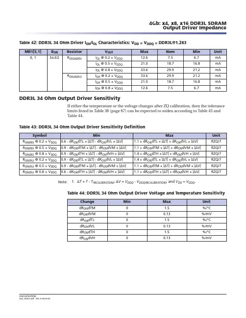
Table 42: DDR3L 34 Ohm Driver I OH/I OL Characteristics: V DD = V DDQ = DDR3L@1.283DDR3L 34 Ohm Output Driver SensitivityIf either the temperature or the voltage changes after ZQ calibration, then the tolerancelimits listed in Table 38 (page 67) can be expected to widen according to Table 43 andTable 44.Table 43: DDR3L 34 Ohm Output Driver Sensitivity DefinitionNote: 1.˂T = T - T(@CALIBRATION); ˂V = V DDQ - V DDQ(@CALIBRATION); and V DD = V DDQ.Table 44: DDR3L 34 Ohm Output Driver Voltage and Temperature SensitivityDDR3L Alternative 40 Ohm DriverTable 45: DDR3L 40 Ohm Driver Impedance CharacteristicsNotes: 1.Tolerance limits assume RZQ of 240˖ ±1% and are applicable after proper ZQ calibra-tion has been performed at a stable temperature and voltage (V DDQ = V DD ; V SSQ = V SS ).Refer to DDR3L 40 Ohm Output Driver Sensitivity (page 70) if either the temperature or the voltage changes after calibration.2.Measurement definition for mismatch between pull-up and pull-down (MM PUPD ). Meas-ure both R ON(PU) and R ON(PD) at 0.5 × V DDQ :MM PUPD = ×100R ON(PU) - R ON(PD)R ON,nom3.For IT and AT devices, the minimum values are derated by 6% when the device operates between –40°C and 0°C (T C ).A larger maximum limit will result in slightly lower minimum currents.DDR3L 40 Ohm Output Driver SensitivityIf either the temperature or the voltage changes after I/O calibration, then the tolerance limits listed in Table 45 can be expected to widen according to Table 46 and Table 47(page 71).Table 46: DDR3L 40 Ohm Output Driver Sensitivity DefinitionNote: 1.˂T = T - T (@CALIBRATION), ˂V = V DDQ - V DDQ(@CALIBRATION); and V DD = V DDQ .Output Characteristics and Operating Conditions Table 48: DDR3L Single-Ended Output Driver CharacteristicsNotes: 1.RZQ of 240˖ ±1% with RZQ/7 enabled (default 34˖ driver) and is applicable after prop-er ZQ calibration has been performed at a stable temperature and voltage (V DDQ = V DD ;V SSQ = V SS ).2.V TT = V DDQ /2.3.See Figure 31 (page 75) for the test load configuration.4.The 6 V/ns maximum is applicable for a single DQ signal when it is switching either from HIGH to LOW or LOW to HIGH while the remaining DQ signals in the same byte lane are either all static or all switching in the opposite direction. For all other DQ signal switch-ing combinations, the maximum limit of 6 V/ns is reduced to 5 V/ns.5.See Figure 28 (page 66) for IV curve linearity. Do not use AC test load.6.See Slew Rate Definitions for Single-Ended Output Signals (page 75) for output slew rate.7.See Figure 28 (page 66) for additional information.8.See Figure 29 (page 73) for an example of a single-ended output signal.4Gb: x4, x8, x16 DDR3L SDRAM Output Characteristics and Operating Conditions。
MT-GSM168无线转发器产品说明书一、无线转发器介绍1.1产品简介令MT-GSMl68无线转发器是一款在工业环境下使用的GSM无线通讯产品,内置高性能GSM模块。
可以广泛应用于电力监控,水利、气象监测,勘探测控等行业和工业领域;本产品采用成熟的GSM无线通讯技术,可使防盗报警主机与接警中心通过GSM无线通讯方式联网。
令由于无线转发器采用工业集成设计,在温度范围、震动、电磁兼容性和接口多样性等方面均采用特殊设计,保证了恶劣环境下的工作稳定性,为您的设备提供高质量保证。
1.2功能特点:令基于德国原装进口模块,工业级设计,EMC设计,具有极高的接收灵敏度和强抗干扰能力,适合长期连续工作。
令可直接匹配任何品牌的报警主机、接警中心、电话机、程控交换机等用户终端设备。
◊安装、设置简单,无需调试,十分适用于野外电塔、水泵站、通信机房、微波发射塔等户外设备的数据通讯,具有高稳定的通讯效果,确保通信畅通无阻。
令实时监控PSTN电话线状态,当电话线发生故障或被剪断时,转发器立即自动切换到GSM工作模式取代电话线,负责通讯、发送报警讯息。
令优美外形配合多功能指示灯,实时反映转发器工作状态,使产品直观易用。
1.3组网应用二、无线转发器使用指南2.1外观结构如右图168(长)Xl12(宽)×28(∣⅛)mm2.2接口说明令电源接口:采用直插式电源座,中芯为中2.5mm AG/X电源功率:29W令天线接口:采用SMA(FEMALE)接口馈入线,外接棒状或吸盘天线。
◊SIM卡插槽:采用抽屉式SIM卡卡座,用户只需用小螺丝刀挤压SIM卡抽屉旁边黄色按纽,SIM卡抽屉即可弹出.将SIM卡对上缺口嵌入抽屉中装回卡座上。
令电话线输入:外接PSTN电话线。
令电话线输出:连接到用户报警主机的电话线输入端,而报警主机的电话线输出端接上用户电话机。
2.3指示灯说明注:3S灭2.4使用说明令正确安装后通上电源,待LED灯自检结束后,GSM状态灯慢闪,转发器已取得网络信号,可以正常工作。
x4 and x8 configurations. The DDR4 SDRAM uses an 8n -prefetch architecture to ach-ieve high-speed operation. The 8n -prefetch architecture is combined with an interface designed to transfer two data words per clock cycle at the I/O pins.A single READ or WRITE operation for the DDR4 SDRAM consists of a single 8n -bit wide, four-clock data transfer at the internal DRAM core and two corresponding n -bit wide, one-half-clock-cycle data transfers at the I/O pins.Industrial TemperatureAn industrial temperature (IT) device option requires that the case temperature not ex-ceed below –40°C or above 95°C. JEDEC specifications require the refresh rate to double when T C exceeds 85°C; this also requires use of the high-temperature self refresh option.Additionally, ODT resistance and the input/output impedance must be derated when operating outside of the commercial temperature range, when T C is between –40°C and 0°C.General Notes•The functionality and the timing specifications discussed in this data sheet are for the DLL enable mode of operation (normal operation), unless specifically stated other-wise.•Throughout the data sheet, the various figures and text refer to DQs as "DQ." The DQ term is to be interpreted as any and all DQ collectively, unless specifically stated oth-erwise.•The terms "_t" and "_c" are used to represent the true and complement of a differen-tial signal pair. These terms replace the previously used notation of "#" and/or over-bar characters. For example, differential data strobe pair DQS, DQS# is now referred to as DQS_t, DQS_c.•The term "_n" is used to represent a signal that is active LOW and replaces the previ-ously used "#" and/or overbar characters. For example: CS# is now referred to as CS_n.•The terms "DQS" and "CK" found throughout the data sheet are to be interpreted as DQS_t, DQS_c and CK_t, CK_c respectively, unless specifically stated otherwise.•Complete functionality may be described throughout the entire document; any page or diagram may have been simplified to convey a topic and may not be inclusive of all requirements.•Any specific requirement takes precedence over a general statement.•Any functionality not specifically stated here within is considered undefined, illegal,and not supported, and can result in unknown operation.•Addressing is denoted as BG[n ] for bank group, BA[n ] for bank address, and A[n ] for row/col address.•The NOP command is not allowed, except when exiting maximum power savings mode or when entering gear-down mode, and only a DES command should be used.•Not all features described within this document may be available on the Rev. A (first)version.•Not all specifications listed are finalized industry standards; best conservative esti-mates have been provided when an industry standard has not been finalized.•Although it is implied throughout the specification, the DRAM must be used after V DD has reached the stable power-on level, which is achieved by toggling CKE at least once every 8192 × t REFI. However, in the event CKE is fixed HIGH, toggling CS_n at least4Gb: x4, x8, x16 DDR4 SDRAM General Notes and DescriptionFigure 108: CRC Error ReportingCK_t CK_cDQ IN ALERT_n Don’t CareTransition Data Notes: 1.D[71:1] CRC computed by DRAM did not match CRC[7:0] at T5 and started error generat-ing process at T6.2.CRC ALERT_PW is specified from the point where the DRAM starts to drive the signal LOW to the point where the DRAM driver releases and the controller starts to pull the signal up.3.Timing diagram applies to x4, x8, and x16 devices.4Gb: x4, x8, x16 DDR4 SDRAM CRC Write Data Feature。
MRW ZQ Calibration CommandsThe MRW command is used to initiate a ZQ calibration command that calibrates output driver impedance across process, temperature, and voltage. LPDDR2-S4 devices sup-port ZQ calibration. To achieve tighter tolerances, proper ZQ calibration must be per-formed.There are four ZQ calibration commands and related timings: t ZQINIT, t ZQRESET,t ZQCL, and t ZQCS. t ZQINIT is used for initialization calibration; t ZQRESET is used for resetting ZQ to the default output impedance; t ZQCL is used for long calibration(s); and t ZQCS is used for short calibration(s). See the MR10 Calibration (MA[7:0] = 0Ah) table for ZQ calibration command code definitions.ZQINIT must be performed for LPDDR2 devices. ZQINIT provides an output impe-dance accuracy of ±15%. After initialization, the ZQ calibration long (ZQCL) can be used to recalibrate the system to an output impedance accuracy of ±15%. A ZQ calibration short (ZQCS) can be used periodically to compensate for temperature and voltage drift in the system.ZQRESET resets the output impedance calibration to a default accuracy of ±30% across process, voltage, and temperature. This command is used to ensure output impedance accuracy to ±30% when ZQCS and ZQCL commands are not used.One ZQCS command can effectively correct at least 1.5% (ZQ correction) of output im-pedance errors within t ZQCS for all speed bins, assuming the maximum sensitivities specified in Table 79 and Table 80 (page 114) are met. The appropriate interval between ZQCS commands can be determined using these tables and system-specific parame-ters.Mobile LPDDR2 devices are subject to temperature drift rate (T driftrate ) and voltage drift rate (V driftrate ) in various applications. To accommodate drift rates and calculate the necessary interval between ZQCS commands, apply the following formula:ZQ correction(T sens × T driftrate ) + (V sens × V driftrate )Where T sens = MAX (dR ON dT) and V sens = MAX (dR ON dV) define temperature and volt-age sensitivities.For example, if T sens = 0.75%/˚C, V sens = 0.20%/mV , T driftrate = 1˚C/sec, and V driftrate =15 mV/sec, then the interval between ZQCS commands is calculated as:1.5(0.75 × 1) + (0.20 × 15) = 0.4s A ZQ calibration command can only be issued when the device is in the idle state with all banks precharged.No other activities can be performed on the data bus during calibration periods(t ZQINIT, t ZQCL, or t ZQCS). The quiet time on the data bus helps to accurately calibrate output impedance. There is no required quiet time after the ZQRESET command. Ifmultiple devices share a single ZQ resistor, only one device can be calibrating at any giv-en time. After calibration is complete, the ZQ ball circuitry is disabled to reduce power consumption.1Gb: x16, x32 Automotive Mobile LPDDR2 SDRAM MODE REGISTER WRITE Commanderation to the entire bank is blocked and bank data retention is not guaranteed in self refresh mode. To enable a REFRESH operation to a bank, the corresponding bank mask bit must be programmed as “unmasked.” When a bank mask bit is unmasked, the array space being refreshed within that bank is determined by the programmed status of the segment mask bits.Partial-Array Self Refresh – Segment MaskingProgramming segment mask bits is similar to programming bank mask bits. For densi-ties 1Gb and higher, eight segments are used for masking (see the MR17 PASR Segment Mask (MA[7:0] = 011h) and MR17 PASR Segment Mask Definitions tables). A mode reg-ister is used for programming segment mask bits up to eight bits. For densities less than 1Gb, segment masking is not supported.When the mask bit to an address range (represented as a segment) is programmed as “masked,” a REFRESH operation to that segment is blocked. Conversely, when a seg-ment mask bit to an address range is unmasked, refresh to that segment is enabled.A segment masking scheme can be used in place of or in combination with a bank masking scheme. Each segment mask bit setting is applied across all banks. For seg-ment masking bit assignments, see the tables noted above.Table 45: Bank and Segment Masking ExampleNote: 1.This table provides values for an 8-bank device with REFRESH operations masked tobanks 1 and 7, and segments 2 and 7.1Gb: x16, x32 Automotive Mobile LPDDR2 SDRAM SELF REFRESH OperationTable 46: Temperature Sensor Definitions and Operating ConditionsMobile LPDDR2 devices accommodate the temperature margin between the point at which the device temperature enters the extended temperature range and the point at which the controller reconfigures the system accordingly. To determine the required MR4 polling frequency, the system must use the maximum TempGradient and the max-imum response time of the system according to the following equation:TempGradient × (ReadInterval + t TSI + SysResp Delay) ≤ 2°CFor example, if TempGradient is 10˚C/s and the SysRespDelay is 1ms:10°C s× (ReadInterval + 32ms + 1ms) ≤ 2°C In this case, ReadInterval must not exceed 167ms.1Gb: x16, x32 Automotive Mobile LPDDR2 SDRAM MODE REGISTER READ。
Programmable Preamble Modes and DQS PostamblesThe device supports programmable WRITE and READ preamble modes, either the nor-mal 1t CK preamble mode or special 2t CK preamble mode. The 2t CK preamble modeplaces special timing constraints on many operational features as well as being suppor-ted for data rates of DDR4-2400 and faster. The WRITE preamble 1t CK or 2t CK modecan be selected independently from READ preamble 1t CK or 2t CK mode.READ preamble training is also supported; this mode can be used by the DRAM con-troller to train or "read level" the DQS receivers.There are t CCD restrictions under some circumstances:•When 2t CK READ preamble mode is enabled, a t CCD_S or t CCD_L of 5 clocks is notallowed.•When 2t CK WRITE preamble mode is enabled and write CRC is not enabled, a t CCD_Sor t CCD_L of 5 clocks is not allowed.•When 2t CK WRITE preamble mode is enabled and write CRC is enabled, a t CCD_S or t CCD_L of 6 clocks is not allowed.WRITE Preamble ModeMR4[12] = 0 selects 1t CK WRITE preamble mode while MR4[12] = 1 selects 2t CK WRITEpreamble mode. Examples are shown in the figures below.Figure 111: 1t CK vs. 2t CK WRITE Preamble Mode2t CK Mode1t CK Mode8Gb: x4, x8, x16 DDR4 SDRAM Programmable Preamble Modes and DQS PostamblesFigure 198: Consecutive WRITE (BC4-Fixed) with 1t CK Preamble and Write CRC in Same or DifferentBank GroupCommand CK_t CK_cDQS_t,DQS_c Don’t CareTransitioning Data Bank Group Address Address DQ x4,BC = 4 (Fixed)DQ x8/X16,BC = 4 (Fixed)Notes: 1.BC4-fixed, AL = 0, CWL = 9, Preamble = 1t CK, t CCD_S/L = 5t CK.2.DI n (or b ) = data-in from column n (or column b ).3.DES commands are shown for ease of illustration; other commands may be valid atthese times.4.BC4 setting activated by MR0[1:0] = 10 during WRITE commands at T0 and T5.5.CA parity = Disable, CS to CA latency = Disable, Read DBI = Disable, Write CRC = Enable,DM = Disable.6.The write recovery time (t WR) and write timing parameter (t WTR) are referenced fromthe first rising clock edge after the last write data shown at T16.8Gb: x4, x8, x16 DDR4 SDRAM WRITE Operation。