ADS8634数据手册
- 格式:pdf
- 大小:1.61 MB
- 文档页数:73

ST ANDARD TVS COMPONENTSAPPLICA TIONS✔ Laptop Computers✔Cellular Phones ✔ Digital Cameras✔ Personal Digital Assistants (PDAs)IEC COMP A TIBILITY(EN61000-4)✔ 61000-4-2 (ESD): Air - 15kV , Contact - 8kV ✔ 61000-4-4 (EFT): 40A - 5/50ns✔ 61000-4-5 (Surge): 24A, 8/20µs - Level 2(Line-Gnd) & Level 3(Line-Line)FEA TURES✔ 500 Watts Peak Pulse Power per Line(td= 8/20µs)✔ Unidirectional & Bidirectional Configurations ✔ Replacement for MLV (0805)✔ Protects One Power or I/O Port✔ Available in Multiple Voltages Ranging From 3.0V to 24.0V ✔ ESD Protection > 40 kilovolts ✔ Low Clamping VoltageMECHANICAL CHARACTERISTICS✔ Molded JEDEC SOD-323✔ Weight 10 milligrams (Approximate)CIRCUIT DIAGRAMSSOD-323UNIDIRECTIONALBIDIRECTIONAL. . . engineered solutions for the transient environment™05118查询PSD03供应商PSD24CDEVICE CHARACTERISTICSNote 1: Part numbers with an additional “C” suffix are bidirectional devices, i.e., PSD05C.Note 2: For Bidirectional Devices Only: Electrical characteristics apply in both directions.ELECTRICAL CHARACTERISTICS PER LINE @ 25°C Unless Otherwise SpecifiedPART NUMBER (See Notes 1-2)DEVICE MARKINGMINIMUM BREAKDOWN VOLTAGE@ 1mA V (BR)VOLTS MAXIMUM CLAMPING VOLTAGE (See Fig. 2)@ I P = 1AV C VOLTS MAXIMUM CLAMPING VOLTAGE (See Fig. 2)@8/20µs V C @ I PP TYPICAL CAPACITANCE0V @ 1 MHzC pFPSD03PSD03C PSD05PSD05C PSD08PSD08C PSD12PSD12C PSD15PSD15C PSD24PSD24CA GB HC JD KE LF M4.04.06.06.08.58.513.313.316.716.726.726.76.57.09.89.813.413.419.019.024.024.043.043.0***********************************************************************************************************************************50020035017525015015050100408840MAXIMUM LEAKAGE CURRENT@VWMI D µA 12512510101010111111RATED ST AND-OFF VOLTAGEV WM VOLTS3.33.35.05.08.08.012.012.015.015.024.024.0MAXIMUM RATINGS @ 25°C Unless Otherwise SpecifiedPeak Pulse Power (td = 8/20µs) - See Figure 1Operating T emperature SYMBOL VALUE -55°C to 150°C°C°C -55°C to 150°C Watts UNITS 500T J P PP T STGPARAMETERStorage T emperature0.01 1 10 100 1,000 10,000t d - Pulse Duration - µs************t - Time - µs20406080100120I P P - P e a k P u l s e C u r r e n t - % o f I P PFIGURE 2101001,00010,000P P P - P e a k P u l s e C u r r e n t - W a t t sFIGURE 1PEAK PULSE POWER VS PULSE TIMEPSD24CT L - Lead T emperature - °C20406080100% O f R a t e d P o w e rFIGURE 3FIGURE 4OVERSHOOT & CLAMPING VOLTAGE FOR PSD05ESD Test Pulse: 5 kilovolt, 1/30ns (waveform)5 V o l t sp e r D i v i s i o n-15-551525FIGURE 50 1 2 3 4 5 6V R - Reverse Voltage - VoltsC - C a p a c i t a n c e - p F100200300400GRAPHSPSD24C P ACKAGE OUTLINE & DIMENSIONSACKAGE DIMENSIONSMILLIMETERSMAX1.901.452.70TAPE & REEL PACKAGING:Surface mount product is taped and reeled in accordance with EIA-481, reel quantites and sizes are as follows:7 Inch Reel - 3,000 pieces per reel; 13 Inch Reel - Not AvailableProTek Devices2929 South Fair Lane, Tempe, AZ 85282T el: 602-431-8101 Fax: 602-431-2288E-Mail:***********************Web Site: COPYRIGHT © ProTek Devices 2001SPECIFICA TIONS: ProT ek reserves the right to change the electrical and or mechanical characteristics described herein without notice (except JEDEC).DESIGN CHANGES: ProT ek reserves the right to discontinue product lines without notice, and that the final judgement concerning selection and specifications is the buyer’s and that in furnishing engineering and technical assistance, ProTek assumes no responsibility with respect to the selection or specifications of such products.。
电力系统配网自动化是一个庞大、复杂、综合性的系统工程,如何将配电网在正常及事故情况下的监测、保护、控制有机地融合在一起,提高供电质量,是电力系统微机保护的一个重要课题;而对配电网的电压、电流参数进行快速、准确地采集,及时反映配电网的故障状态并进行相应处理,是配电系统微机保护的首要任务。
使用美国德州仪器公司(TI)推出的ADS8364 A/D芯片与TMS320LF2407DSP芯片构成控制系统是一个较好的解决方案,现已将其成功应用到配电网中。
本文在简介ADS8364和TMS320LF2407的功能、性能和特点的基础上,介绍ADS83 64与TMS320LF2407的硬件接口电路和软件编程方法。
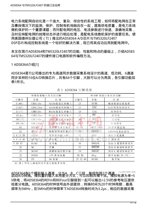
1 ADS8364介绍[1]ADS8364是TI公司推出的专为高速同步数据采集系统设计的高速、低功耗、6通道同步采样的16位A/D转换芯片,共有64个引脚,大致可以分为两类,各引脚功能如表1所示。
ADS8364有6个模拟输入通道,分为A、B、C三组,每组包括2个通道,启动A/D转换。
模拟量的输入采用差分方式,可以抑制共模干扰。
模拟电源为单+5 V供电,将ADS8364的REFin和REFout引脚接到一起可以输出+2.5V的参考电压提供给差分电路。
ADS8364的时钟信号由外部提供,转换时间为20个时钟周期,最高频率为5MHz,在5MHz的时钟频率下ADS8364转换时间为3.2μs,相应的数据采集时间为0.8μs,每个通道的总的转换时间为4μs,A/D转换完成后产生转换结束信号数字电源供电电压为3V~5V,即可以与3.3V供电的微控制器接口,也可以与5V供电的微控制器接口。
A/D转换结果为16位,最高位为符号位,数据输出方式很灵活,分别由BYTE、ADD与地址线A2A1A0的组合控制,如表2所示。
从表2中可以看出,转换结果的读取方式有三种:直接读取、循环读取和FIFO方式。
根据BYTE为0或者为1可确定每次读取时得到的数据位数,根据ADD为0或者为1可确定第一次读取的是通道地址信息还是通道A/D转换结果。

Agilent EEsof EDAAdvanced Design SystemFor Designs that Live Up to Your Dreams“We were pleasantly surprised to learn that Agilent EEsof EDA offers affordable choic-es for growing compa-nies like us. They set the standard for high-frequency design soft-ware and have the broadest range of simu-lation capabilities. I'm confident that we have chosen a toolset that can expand with us as we grow.” Steven J. Bennett Vice President of Research andDevelopment, UnityWireless SystemsIn Gary Smith EDA’s 2009 market share report, Agilent EEsof wasrecognized as the leading provider of RF Design and Simulation tools.For designs that live up to your dreams,choose software that lives up to your designsAs technology and competition acceler-ate, so do the challenges of getting to market first, with better, smaller, and fast-er products. Today, it is critical for engi-neers to be productive and effective. Efficiently exploring different design pos-sibilities requires powerful tools and meth-odologies.Agilent understands these challenges first-hand. Our diverse electronic products and test and measurement businesses include designers of RF and microwave semiconductor products such as duplex-ers, filters, mixers, and RFICs. Our own fabrication facilities include Si and GaAs processes for manufacturing circuits and components such as mixers, attenuators, prescalers, switches, and power amplifier ICs – all used extensively in today’s sophisticated communications products. Our EDA business grew out of an internal need to improve the design process for RF and microwave test instrumentation. The business quickly grew to division sta-tus, with a long history of innovation that continues today, including many patented technologies and current patents pending. With the introduction of the Touchstone linear simulator more than 20 years ago, Agilent EEsof EDA has led the develop-ment of new high-frequency EDA technol-ogies such as Harmonic Balance and Circuit Envelope simulators, RF/analog/baseband co-simulation and behavioralMost popular high-frequency design softwareAdvanced Design System (ADS) is the industry leader in high-frequency design. It supports system and RF design engineers developing all types of RF designs, from simple to the most complex, from RF/microwave modules to integrated MMICs for communications and aerospace/defense applications. With a complete set of simulation technologies ranging from frequencyand time-domain circuit simulation to electromagnetic field simulation, ADS lets designers fully characterize and optimizedesigns. The single, integrated design environment provides system and circuit simulators, along with schematic capture, layout, and verification capability – elimi-nating the stops and starts associated with changing design tools mid-cycle. Agilent EEsof EDA offers a wide variety of flexible plans to work within your budget. Time-based licenses and limited-term packages are available to get you the tools you need today. As your design needs grow, you can add simulators,models, and libraries as you require them.models. It is technology that has proven its robustness and lasting value over time.More focus on design – less on learningTime-to-market pressures often don’t accommodate learning a new software package. To help designers get to first-cut design results, ADS supplies over 300 examples or start from templates. ADS supplies over 300 examples, accessed through a powerful search engine. Each example gives instructions for using ADS, enabling you to focus on the design, and not on the design tool.Data display for the big pictureIf your simulation results do not allow you to see at a glance how your design is performing, you’re losing productivity. The strong data analysis and display technology in ADS lets you view results in the many ways you may want tosee them. Post processing capabilitiesDesignGuides for expert helpAgilent EEsof EDA has more than a dozen industry experts using theirexperience and best practices to create application-oriented ADS DesignGuides. DesignGuides make the job of circuit design easier, faster, and more consistent with wizards, pre-configured set-ups and displays, and step-by-step instructions. Complete design applications such as amplifiers, filters, mixers, microstripcircuits, RF systems, Bluetooth, and ultra-wideband designs, to name just a few, give you easy access to the power of ADSwithout taking time to learn from scratch.“I collaborate with Agilent EEsof EDA because they have the largest customer base to potentially benefit from my expertise. The open architecture of the ADS platform makes it easy for application specialists like me to develop DesignGuides. The time I put into a DesignGuide is time saved in engineering cycles.”Dr. Michael Jensen Professor of Electrical Engineering, Brigham Young University and Vice President of AJ Design GroupDesignGuides and templates in ADS make displaying simulation results easy.The ADS optimization cockpit provides an interactive environment with multiple optimization variables, interactive tuning and progress controls. Achieve the best performance while gaining design insight of the optimized variables versus the goals.let you manipulate data using custom expressions, view data on different plots, and change specifications, all without re-simulating.Design Libraries for easier wireless designFor cutting-edge wireless design, ADS Design Libraries help get emerging wire-less products to market faster. By building the latest signal formats into ADS, you can spend your time on new design ideas, not on researching the standards. Design Libraries contain pre-configured schemat-ics, data displays, and test benches to help you verify designs against measure-ments defined in the wireless standards specifications.The widest choice in models– from Process Design Kits to custom extractionDesign kits for foundry process compatibilityAgilent works with top foundries around the world to develop and support process design kits for RFIC and MMIC design in ADS. Kits are maintained by the foundry,so you can be sure they provide the most accurate and up-to-date models for their latest process, as well as the most com-prehensive design automation features.High-quality models for accuracyAccurate models are a prerequisite for any successful design flow. Without good models, designers can’t make progress or have confidence in their simulation results.ADS has models for every microwave and RF design application:• RF System models provide gain blocks, mixers, filters, modulators and demodu-lators, PLL components, and passive elements for accurate and easy system design.• All the major component vendorsprovide up-to-date component libraries specifically for ADS.• Component libraries have over 100,000 parts. Many contain auto-layout capa-bilities for creating a layout directly from schematic for design rule check-ing or planar EM simulation.• Design Libraries contain models for the latest communication standard modu-lation formats, including 3GPP LTE, HSPA, Mobile/Fixed WiMAX™, DTMB, CMMB, WVAN, CDMA, GSM, DTV, 802.11n, TD-SCDMA, WLAN, W-CDMA, CDMA2000/1xEV, EDGE, WiMedia.Several options allow you to develop cus-tomized models that meet your specific device and product requirements:• Advanced Model Composer, based on a patented technology, uses EM simulation to create accurate passive models that have the simulation speed advantages of analytical models.• Verification Model Extractor creates system-level behavioral models from device-level circuit designs for faster system-level verification.• Analog Model Development Kit gener-ates user-defined circuit and system models for integrating proprietary behavioral models.• Verilog-A compiler allows the simula-tion of custom device models and behavioral models in Verilog-A format.Agilent also provides modeling systems to develop accurate device model extrac-tions.“ADS is an important toolset to support. It has the widest usage among our customer base and within TriQuint.”Eli Reese Director ofDesign Engineering at TriQuint Semiconductorin Richardson, Texas.AC/S-Parameters High Speed Interconnect LibraryHarmonic BalanceCo-Simulation with 3rd Party Simulators Agilent Ptolemy Timed Synchronous DataflowCircuit EnvelopeTransient ConvolutionMomentumP h y s i c a lN u m e r i cT i m eF r e q u e n c yAdvanced Model ComposerFinite ElementADS Simulation TechnologyAdvancing TechnologyD o m a i nIndustry-leading simulation technology – circuit to system, simple to complexSimulator technology handles size, complexity, with easeDesigning circuits for different functional blocks often requires an array of simula-tion technologies. ADS offers the most complete set of simulation technologies available today in a single software pack-age. Combined, they enable you to fully characterize and optimize designs under varied conditions without simulator-imposed limitations on accuracy, depth, or detail. The result is a design that can exceed performance requirements and be manufactured at high volumes.Simulator highlights:• For system-level simulation, Agilent Ptolemy is the only commercially available timed synchronous data flow co-simulate with the analog and RF simulators, allowing you to see the effects that circuit-level blocks have on system-level results, for a true mixed-signal analysis.• When it was introduced in the early 1980s, Harmonic Balance was the first commercially available simulator of its kind. Over time, it has developed into the most advanced frequency-domain simulator for fast analysis of nonlinear circuits. Today, it can handle large-scale ICs with thousands of transistors. It also simulates digital frequency-divider circuits using the Transient Assisted Harmonic Balance capability.• C ircuit Envelope is a patented ADS innovation that enables accurate analy-sis of time-varying carriers directly in the frequency domain. Only Circuit Envelope simulates time-varying signal response at the system level, allowingdirect and easy optimization of circuit performance. Key applications include modulator/ demodulator response, synthesizer hopping analysis, phase-lock-loop-based automatic frequency control response, oscillator stability and warm up, and automatic gain control/phase-lock-loop response to complex signals.• The RF System simulator contains a unique RF system budget analysis feature that lets you examine more than 40 system measurements such as third-order intercept, 1dBc, and noise figure for each component in the high-level system.The time-based Transient/Convolution simulator accounts for frequency- domain effects such as coupled transmission lines.ADS Layout information is combined with the Momentum substrate definition to produce a 3D spatial representation of circuit geometries.Co-simulation with LayoutComponents allows you toincorporate layout artwork inthe schematic environmentto enable concurrent analy-sis of circuit performancealong with critical physicaleffects.The Physical Connectivity Engine check connectivity fea-ture allows you to highlight any trace or interconnect. Itthen highlights all overlapping metal.From the spark of an idea to a verified design –Agilent EEsof EDA is committed to providing the most complete design flow. Where gaps exist that give designers pain and take up their time, we round out our product line and solutions to bridge them. Physical design predicts performanceAccurate implementation of physical design is important for predicting hard-ware performance. ADS includes a com-prehensive physical design environment specifically geared for high-frequency layout design and verification. It hostsa number of capabilities such as design synchronization with schematic, a physi-cal connecivity engine, integrated EM simulators, and a design rule checker (DRC). Layout allows designers to fully characterize artwork and improves the ability to catch errors prior to production. Physical Connectivity EngineWhen it comes to high-frequency design,traditional LVS tools often limit intercon-nect options to simple traces. Agilent’sPhysical Connectivity Engine lets you useany custom shape to build interconnects.The engine runs in the background andextracts interconnect information fromtraces, paths, vias, and custom polygons,in real time, allowing you to perform anumber of interconnect checks withoutlaunching a separate utility. The PhysicalConnectivity Engine also allows you toverify real-time-connectivity graphically onyour layout, providing a true representa-tion of interconnects. Better interconnectrepresentations reduce design uncertaintybefore prototyping, so you can be confi-dent that what you design in schematic iswhat you represent in layout.Momentum & FEM Simulatorfor EM AnalysisBoth Agilent’s Momentum and FiniteElement Method (FEM) simulators arefully integrated with the ADS layoutenvironment. Momentum is the leading3D planar electromagnetic (EM) simulatorused for multi-layer IC and PC Boardanalysis. The FEM simulator is based onfull 3D EM technology that can handle3D arbitrary shaped structures suchas connectors, conical shape vias andsolder balls/bumps where z-dimensionalchanges appear in the structure. Bothsimulators generate accurate EM modelsthat can be used directly with ADS circuitsimulators.Agilent’s X-parameters* represent a new category of nonlinear network parameters for high-frequency design. They are applicable to both large-signal and small-signal condi-tions, and for linear and nonlinear components.– with no break in the flowConnected SolutionsDesign verification using today’s complex communications signal formats is a chal-lenge. Designs can be analyzed early in simulation, and they can be verified later, after all of the hardware returns from fabrication – but designers don’t have the luxury of waiting for all of the hardware. They need an intermediate level of verification to cut overall design time and reduce risk.Agilent’s connected solutions allow verification very early in the prototyping cycle for applications ranging fromemerging wireless communications prod-ucts to aerospace/defense by integrating ADS with Agilent test instruments such as signal generators and signal analyzers to enable new design and verification capabilities. This unique combination allows the sharing of signals, measure-ments, algorithms, and data seamlessly between the virtual software and physical hardware domains. Designers use this linkage to simulate and evaluate design trade-offs and what-ifs and then turn the simulated signal into an RF test signal on the bench f or hardware test. Conversely, designers can take themeasured output signal from the DUT and bring it into ADS for additional analysis in the simulation environment.Design flow integration – partners for complete successAt Agilent EEsof EDA we align with key EDA vendors and frameworks to provide enhanced solutions that complement your investment. The open and flexible ADS environment ensures that a wide range of design flows is supported. For example, if your design flow is based on a Cadence, Mentor or Zuken flow, Agilent EEsof EDA supports these frameworks with integra-tion products using industry-standard formats. Our expanding list of partners goes well beyond standard relationships and is part of an ongoing effort to provide best-in-class tools and technology that work the way you work best—in anintegrated environment.New X-Parameter GeneratorX-parameter models are fast, cascadable,nonlinear behavioral models thataccurately account for frequency mixing and impedance mismatch. X-parameters fulfill a long standing need from the high-frequency design community for nonlinear behavioral models that can be created from measurement or simulation with the same speed and convenience as the well known linear S-parameters. The X-Parameter Generator enables MMIC,RF-SIP and RF module design houses to provide their customers with an accurate,pre-prototype model of their nonlinear devices (e.g. power amplifiers, front-end modules and transceivers) to further enable concurrent design and secureearly design wins.“Agilent’s design software and test hardware accelerates our design verification,giving us the confidence to begin prototyping”Eric HansenPresident and CEO of Innovative Wireless TechnologiesApplication Areas– from RF to microwave, from circuit to system,Microwave/MMIC design Reduce costs and get to market fast, and first. This is the challenge that MMIC designers face. ADS rises to this chal-lenge, making MMIC design faster and easier than ever before. ADS supports a complete, front-to-back flow by incorpo-rating Layout and all of the ADS simula-tion technologies (system, circuit, and electromagnetic) in a single, integrated design flow. All of today’s leading GaAs foundries actively maintain component design kits that support the powerful ADS simulation technologies.In microwave circuit design, the circuit and physical designs must be closely linked. ADS allows you to start a MMIC design in either the layout or schematic environment. The design synchronization engine controls and tracks design updates and supports multiple design synchronization modes to match your methodology.The ADS Layout components feature adds a new dimensionto MMIC design.You can bring alayout directly intothe schematicenvironment to giveyou access to EMsimulators withinyour circuit design.Or, you can bringin a DUT board –characterized bynetwork analyzermeasurements orby EM simulation– for concurrentmodeling of thedesign whileaccounting forboard or packagingeffects. Signal integrity/high-speed digital designSignal integrity is a major concern forengineers of high-data-rate designs, suchas Infiniband, PCI Express, and RapidIO.Meeting the demand for increasinglyfast circuits with high clock speeds is aconstant challenge. High-frequency ana-log effects such as reflection, cross talk,ground bounce, and propagation delaysthrough interconnects adversely affectsignal quality and timing performance.ADS has the right simulation tools andlibraries, including a multi-layer intercon-nect library that enables you to accuratelymodel and analyze high-speed intercon-nect problems before fabrication, resultingin lower development costs and fastertime to market.RFIC designAs today’s wireless and wireline applica-tions increase in frequency and speed,RFIC design engineers need access toaccurate and efficient high-frequencysimulation tools. Shorter product life-cycles and global competition continue toadd pressure for quality product designs.Agilent EEsof EDA has the most compre-hensive set of simulation tools, models,and verification features to increase therobustness of your RFIC designs.If your designs are based on the Cadenceflow, you can access Agilent’s powerfulfrequency-domain simulation technolo-gies directly from within the Cadenceenvironment using Agilent’s GoldenGate.Circuit netlists from the Cadence environ-ment can also be brought into ADS foranalysis using Dynamic Link. Either way,you’ve got the power to efficiently designRFICs with high performance and yield forcapitalizing on market opportunities.The Complete MMIC ADS Desktop Design Flow enable front-to-back design and simulation to physical design, verification and manufacturing.from board to package to RFIC – ADS is the tool of choiceCommunications system designToday, the complexities of system design are greater than ever. Designers working with recent and emerging wireless stan-dards such as 3GPP LTE, HSPA, Mobile/ Fixed WiMAX™, DTMB, CMMB, WVAN, CDMA, GSM, DTV, 802.11n, TD-SCDMA, WLAN, W-CDMA, CDMA2000/1xEV, EDGE, WiMedia, need to reduce design turns and get to market quickly with a complete system that satisfies the needs of RF/analog and baseband applications. Aerospace/defense industry designers also need quick design turns and rapid design verification when specifications are incomplete and measurements are highly specialized.Wireless communications product system designs must be partitioned into their baseband and RF portions. For the RF portion, ADS provides more behavioral models than any other EDA vendor – more than 1800 models in all. ADS design and model libraries are preconfigured for simulation and contain the most complete set of measurements available. When additional measurements are required, Connected Solutions fills the gap with signal generation, sharing, and analysis via instrument-software links.In aerospace/defense, Agilent’s con-nected solutions are particularly useful for extending the standard measurements provided by Agilent’s test instruments by combining them with ADS and its exten-sive library of behavioral models. RF Board designToday’s high-frequency RF board designerwants few board re-spins and high-yield designs. The integrated system,circuit, and EM simulators, Layout, andpowerful optimizers in ADS help increaseproductivity and efficiency, validating yourhigh-yield designs prior to manufacturing.Our focus on design flow integrationmeans that ADS works with your otherframework integration products, such asMentor, Cadence and Zuken.Integration also means that the ADSLayout tool is linked to the schematicenvironment. This back-annotating link,coupled with our integrated EM simulator,allows you to account for physical effectsthat could significantly affect designperformance. The Physical ConnectivityEngine detects wiring information that isso important to a correct layout, and feedsit to the interconnect checking featuresin ADS for an accurate representation oflayout interconnects.A growing list of up-to-date componentlibraries is available for ADS RF boarddesign. Agilent, component vendors, andmodeling companies regularly updatethese libraries, and we provide downloadaccess to them via the Agilent EEsof EDAweb site.An ever growing list of component vendorsprovide libraries for ADS. (Several of theseare offered by Modelithics, Inc.)• On Semiconductors• Panasonic• Philips• Polyfet• Presidio Components Inc.• Samsung• Samtec• SAMYOUNG• Skyworks• Taiyo Yuden• Temwell• TDK• Thin Film Technology (TFT)• Toko• Toshiba• Transcom• VishayGetting the most from ADSWorld-class supportyou need to ensure that support will be there when and where you need it. Agilent EEsof EDA has dedicated support engineers in many countries to provide you with local language support, including English, Japanese, Korean, Mandarin, French, German, and Dutch. Phone sup-port is available Monday through Friday, worldwide.of the way. They include software and user manual updates via download or on CD-ROM, worldwide technical support via telephone, fax, e-mail, and the worldwide web.In a world where not only your product goes international, but often your design team is also distributed across continents,Knowledge CenterIn the Knowledge Center, Maintenance Service Releases – with updates to previ-ously released software versions – are available for download. A tracking feature allows you to submit and manage your support cases and related defect and enhancement requests. A robust search function lets you quickly find available solutions and sort through them by date,popularity, or user ratings. The Knowledge Center also contains product discussion forums where you can converse with other users, support engineers, and product developers, along with recorded Technical Info Sessions and introductory e-Learning Short Courses.The Agilent EEsof EDA support web site, featuring the Agilent EEsof Knowledge Center, is an around-the-clock resource for designers. The Knowledge Centercontains thousands of support documents and hundreds of downloadable examples created by support engineers to supple-ment the ADS application examples and documentation.Agilent Technologies is committed to customer satisfaction. We are dedicated to providing the right software, support, and consulting solutions to increase your engineering productivity and advance your long-term success. Whether you are a novice or experienced user, Agilent EEsof EDA’s customer support offerings are designed to help you every step11Achieve business results faster with help from the expertsEvery design team’s flow has aspects that are unique. To save time and get indi-vidual attention focused on your particular design needs, take advantage of Agilent EEsof EDA’s consulting services. We offer complete consulting in MMIC, RFIC, RF board/module, or system-level design.• Device Modeling – We can quickly characterize and extract industry-stan-dard models for your device, and then (optionally) provide test structure and device layout design services.• P rocess Design Kits – Let us create or extend your custom PDK elements or libraries.• C onnected Solutions – Get start-up training in simulation plus instrumenta-tion set-up for X-parameters, 3G, LTE.• Simulation Assistance – Eliminate trial and error. Get expert coaching and learn best practices for complex circuits or systems.• Design Process Consulting – Let us perform an analysis of your design flow and make recommendations that will save you time and money.– with support, training, servicesTrainingHaving a good working knowledge of your EDA software can save precious time in the design cycle. Increased productivity and added expertise can contribute directly to your job satisfaction and to your company’s bottom line.Agilent EEsof EDA training offers a full range of classroom courses, as well as live and self-paced e-learning courses that teach the use of EDA software in a wide variety of applications. Live classes are conducted by experienced design engineers and focus on in-depth software operation and design examples, as well as covering introductory and advanced microwave, RF, System, and signal integrity design techniques. Self-paced e-learning courses allow you to set your own timetable. If you can’t travel to a regularly scheduled class and have agroup of designers who can benefit from a common class, your field sales represen-tative can arrange an on-site class.“I really appreciate the Agilent EEsof EDA training class.The presentation of ADS capabilities,such as how to simulate an entire communication link and integrate RF with Ptolemy, is excellent.”Peter DenneyRF/Antenna Engineer,Harris CorporationFor more information on AgilentTechnologies’ products, applications or services, please contact your local Agilent office. The complete list is available at:/find/contactus Americas Canada (877) 894 4414 Brazil (11) 4197 3500Mexico 01800 5064 800 United States (800) 829 4444Asia Pacific Australia 1 800 629 485China 800 810 0189Hong Kong 800 938 693India 1 800 112 929Japan 0120 (421) 345Korea 080 769 0800Malaysia 1 800 888 848Singapore 1 800 375 8100Taiwan 0800 047 866Other AP Countries (65) 375 8100 Europe & Middle East Belgium 32 (0) 2 404 93 40 Denmark 45 70 13 15 15Finland 358 (0) 10 855 2100France 0825 010 700**0.125 €/minuteGermany 49 (0) 7031 464 6333 Ireland 1890 924 204Israel 972-3-9288-504/544Italy39 02 92 60 8484Netherlands 31 (0) 20 547 2111Spain 34 (91) 631 3300Sweden0200-88 22 55United Kingdom 44 (0) 118 9276201For other unlisted Countries:/find/contactusRevised: October 14, 2010Product specifications and descriptions in this document subject to change without notice.© Agilent Technologies, Inc. 2001-2010Printed in USA, November 9, 20105988-3326EN/find/adsGet what you need today, with an eye to what you’ll need tomorrowExtensible design suites let you begin with a front-to-back solution that fits your budget, adding capabilities as you need them. ADS products range from eco-nomical foundation toolsets to advanced,comprehensive suites. Time-basedlicenses and limited-term packages also are available to give you the tools youneed just when you need them.ADS BundleIntegral to ADS CorePre-configured Element capabilities Provide powerful cost-effective functionalityADS Bundles come in different sizes and configurations to suit your design needsADS EnvironmentSimulators Design GuidesInstrument ConnectivityLayout ElementHarmonic Balance Element Momentum G2 ElementADS Product StructureThe flexible product structure of ADS lets you begin with pre-configured bundles and add capabilities as you need them.。


Leading Innovator in Power Testing Solution用户手册ASD863+651多协议多通道可编程智能交直流测试设备©版权归属于昂盛达电子有限公司Ver1.0 /NOV, 2020/ ASD863+651目录第一章验货安装 (4)1.1验货 (4)1.2清洁 (4)1.3连接部分的安装 (4)1.4安装尺寸 (4)1.5安装位置 (4)第二章快速入门 (5)2.1自检 (5)2.2负载仪前面板介绍 (6)2.3负载仪后面板介绍 (6)2.4功率计前面板介绍 (7)2.5功率计后面板介绍 (7)2.6测试治具介绍 (8)2.7触控屏介绍 (8)第三章技术规格 (9)第四章设备连接 (11)4.1测试设备环境搭建 (11)4.2待测试产品接口 (12)第五章基本操作 (13)5.1开机 (13)5.2研发模式 (14)5.3自动模式(A LONE测试模式) (16)5.4自动模式(2&2测试模式) (23)5.5自动模式(4IN1测试模式) (23)5.6其他设置 (24)第六章常见问题 (25)第七章保修协议 (26)简介ASD863+651交直流测试设备由ASD863多协议负载仪,ASD651 PF数字功率计,安卓操作终端三部分组成,主要用于电源适配器等外接电源PCBA和成品的功能检测、参数测试及性能评估。
负载仪内部集成4个独立的可编程多协议电子负载模块,在具备普通电子负载仪基础功能上同时兼容QC、PD快充协议.PF数字功率计集成4个独立AC交流测试模块和隔离变压器,单台设备可完成PCBA或成品的大部分功能测试,测试快充时无需诱骗器等辅助设备。
支持导入或导出文件,可将测试结果以文档形式直接导出到U盘等USB存储设备。
支持手动研发模式和自动测试,既适用于研发调试和性能评估,亦便于生产线批量检测使用。
特性●15.6寸高清液晶触摸屏,安卓系统上位机操作界面;兼容标准,QC、PD、PPS、AFC、FCP、SCP、SSCP、VOOC、SVOOC等协议●支持手动调试界面,操作简单,功能全面;●支持自动测试,可设定系列参数后一键快捷测试,方便产线批量检测;●AC端测试:支持多档电压切换输入,测试AC电流、功率、功率因素和转换效率;●负载测试:快充适配器PCBA 和成品的输出电压、电流、功率,纹波的测试;●支持恒流模式(CC)和恒压模式(CV)切换;●4通道8端口输入,4切4左右通道切换。
Agilent8643A, 8644B, 8664A, 8665A/BHigh Performance RF Signal GeneratorsData SheetA commitment to value in signal generators1981Agilent’s high performance RF signal generators – choose one for……Best price to performance•252 kHz to 1030 MHz, 2060 MHz Option 002•For out-of-channel tests•Electronic attenuator for high use•Lowest cost of the "family"•AM, FM, pulse modulation•Built-in 2 GHz counter (Option 011)•VOR/ILS signal simulation (Option 009)•Ultra low leakage (Option 010)…Best spectral purity•252 kHz to 1030 MHz, 2060 MHz Option 002•Lowest SSB phase noise and spurious•Highest output power•Lowest residual FM•AM, FM, pulse modulation•Built-in 2 GHz counter (Option 011)•VOR/ILS signal simulation (Option 009)•Ultra low leakage (Option 010)…High RF frequency coverage•100 kHz to 3000 MHz - 8664A, 4200 MHz - 8665A, 6000 MHz - 8665B•Low SSB phase noise (Option 004)•AM and wideband FM•High performance pulse modulation (Option 008)•Ultra low leakage (Option 010)1.For FM receivers with approximately 14 kHz IF BW and 25 kHz channel spacing3Performance backed by Agilent’s reputation and manufacturing experience4Typical performance, for applications that push specificationsSSB phase noiseSSB phase noise is an important specifica-tion of a signal generator if it is to be used for measuring the adjacent channel selec-tivity of a receiver. If the phase noise of the signal generator is too high at frequency offsets equal to the channel spacing, the test results might indicate a failure of the receiver when it is actually functioning properly. For a receiver with <90 dB of selectivity the 8643A is recommended. If the selectivity is ≥90 dB, the 8644B (or 8664A with Option 004, or 8665A/B Option 004) is recommended.Output level accuracyOutput level accuracy is a combination of temperature variation, flatness over fre-quency, and the signal generator’s internal attenuator and detector accuracies. The graph represents worst case output level accuracy of a sampling of 8665Bs. All of these units fall within the shaded area. RF leakageDue to radios becoming more sensitive and operating at higher frequencies, the traditional two-turn loop measurement of RF leakage has become inadequate. To overcome the shortcomings of the two-turn loop, Agilent has developed a new measurement technique using resonant dipole antennas, which is 20-25 dB more sensitive than the two-turn loop method. Agilent has been able to reduce the level of radiated emissions in its newer signal generators through innovative design and packaging. Understanding that not all applications require the lowest possible emissions, Option 010 is available on all of these performance signal generators.Typical SSB phase noise and spurs at 1 GHZ8664A 8665A/BstandardOption 004-60-80-100-120-140-16010 100 1K 10K 100K 1M 10MSSBphasenoise(dBc/Hz)(f) [dBc/Hz] vs. f[Hz]Typical SSB phase noise and spurs at 1 GHZ8643A8644B-60-80-100-120-140-16010 100 1K 10K 100K 1M 10M 40MSSBphasenoise(dBc/Hz)(f) [dBc/Hz] vs. f[Hz]5Internal modulation source •Low distortion sinewaves to 400 kHz with variable phase and amplitude.•Triangle, sawtooth and squarewaves to 50 kHz with variable phase and amplitude.•White Gaussian noise with variable amplitude.•Two independent sources for two-tone testing.Optional pulse modulation(Option 008, 8664A and8665A/B)•An Agilent designed GaAs pulsemodulator provides the exceptionalperformance that is so critical for pulsedapplications.•<5 ns rise/fall times, >80 dB on/offratio.•Built-in pulse generator featuresinclude variable pulse delay and widthfrom 50 ns to 999 ms. This savespurchasing additional equipment.•Leveled RF output maintains accuracywhile in pulse modulation.High reliability electronicattenuator on the 8643A(optional on 8644B)For applications up to 1 GHz, the electronicattenuator used in the 8643A providesincreased reliability. Instead of usingmechanical relays, the electronic attenuatoruses solid-state components for settingoutput levels accurate to within ±1.0 dB.The Agilent patented design uses PINswitching elements with three millionhours of MTBF, giving the attenuator anestimated 0.2% failure rate.Features that improve the usability of Agilent’s 8643A, 8644B, 8664Aand 8665A/B for your application!6Wideband FM (8664A and 8665A/B)•Typical rates to 5 MHz with 2 MHz of deviation, or rates to 800 kHz with10 MHz of deviation (f c>1500 MHz) allows testing of most wideband receivers.•Excellent FM linearity is inherent due to YIG oscillator design.•Stable dc-coupled FM for measurements that require low carrier drift.Performance signal generatorseries features•High stability oven controlled timebaseis standard.•Surface mount construction forimproved reliability.•Three year calibration cycle (MTBC)means less time in the calibration lab.•Built-in self-diagnostics and calibrationsaves valuable time by significantlyreducing down time.2 GHz frequency counter(Option 011, 8643A and 8644B)•20 Hz to 2 GHz frequency counting viafront panel connector.•Cost and space efficient solution forapplications involving audio frequencymeasurements, local oscillator, IF andtransmitter testing.•Eliminates the need to externally couplethe timebase references when using anexternal counter.7Specifications1.3000 MHz for 8664A, 4200 MHz for 8665A, 6000 MHz for 8665B. 8Specifications (continued)1.3000 MHz for 8664A, 4200 MHz for 8665A, 6000 MHz for 8665B.2.One watt on 8665B.3.Low noise mode three.9Specifications (continued)10Specifications (continued)11Agilent Technologies’ Test and Measurement Support, Services, and AssistanceAgilent Technologies aims to maximize the value you receive, while minimizing your risk and problems. We strive to ensure that you get the test and measurement capabilities you paid for and obtain the support you need. Our exten-sive support resources and services can help you choose the right Agilent products for your applications and apply them successfully. Every instrument and system we sell has a global warranty. Support is available for at least five years beyond the production life of the product. Two concepts underlie Agilent’s overall support policy: “Our Promise” and “Your Advantage.”Our PromiseOur Promise means your Agilent test and meas-urement equipment will meet its advertised performance and functionality. When you are choosing new equipment, we will help you with product information, including realistic perform-ance specifications and practical recommenda-tions from experienced test engineers. When you use Agilent equipment, we can verify that itworks properly, help with product operation,and provide basic measurement assistance forthe use of specified capabilities, at no extra costupon request. Many self-help tools are available.Your AdvantageYour Advantage means that Agilent offers awide range of additional expert test and meas-urement services, which you can purchaseaccording to your unique technical and busi-ness needs. Solve problems efficiently and gaina competitive edge by contracting with us forcalibration, extra-cost upgrades, out-of-warran-ty repairs, and on-site education and training,as well as design, system integration, projectmanagement, and other professional engineer-ing services. Experienced Agilent engineers andtechnicians worldwide can help you maximizeyour productivity, optimize the return on invest-ment of your Agilent instruments and systems,and obtain dependable measurement accuracyfor the life of those products.For more assistance with your test andmeasurement needs go to:/find/assistOr contact the test and measurement expertsat Agilent Technologies(During normal business hours)United States:(tel)180****4844Canada:(tel)187****4414(fax) (905) 206 4120Europe:(tel) (31 20) 547 2000Japan:(tel) (81) 426 56 7832(fax) (81) 426 56 7840Latin America:(tel) (305) 267 4245(fax) (305) 267 4286Australia:(tel) 1 800 629 485(fax) (61 3) 9272 0749New Zealand:(tel) 0 800 738 378(fax) 64 4 495 8950Asia Pacific:(tel) (852) 3197 7777(fax) (852) 2506 9284Product specifications and descriptions in thisdocument subject to change without notice.Copyright © 2001 Agilent TechnologiesPrinted in the USA, April 30, 20015091-2580E12。
©1997 Burr-Brown Corporation PDS-1441C Printed in U.S.A. June, 1998®2ADS7843PARAMETER CONDITIONSMIN TYPMAX UNITSANALOG INPUTFull-Scale Input Span Positive Input - Negative Input0V REF V Absolute Input Range Positive Input –0.2+V CC +0.2V Negative Input–0.2+0.2V Capacitance 25pF Leakage Current0.1µA SYSTEM PERFORMANCE Resolution12Bits No Missing Codes 11Bits Integral Linearity Error ±2LSB (1)Offset Error±6LSB Offset Error Match 0.1 1.0LSB Gain Error±4LSB Gain Error Match 0.1 1.0LSB Noise30µVrms Power Supply Rejection 70dB SAMPLING DYNAMICS Conversion Time 12Clk Cycles Acquisition Time 3Clk CyclesThroughput Rate125kHz Multiplexer Settling Time 500ns Aperture Delay 30ns Aperture Jitter100ps Channel-to-Channel Isolation V IN = 2.5Vp-p at 50kHz100dBSWITCH DRIVERS On-Resistance Y+, X+5ΩY–, X–6ΩREFERENCE INPUT Range1.0+V CC V Resistance CS = GND or +V CC 5G ΩInput Current1340µA f SAMPLE = 12.5kHz2.5µA CS = +V CC0.0013µADIGITAL INPUT/OUTPUT Logic FamilyCMOSLogic Levels, Except PENIRQ V IH | I IH | ≤ +5µA +V CC • 0.7+V CC +0.3V IL | I IL | ≤ +5µA –0.3+0.8V V OH I OH = –250µA +V CC • 0.8V V OL I OL = 250µA0.4V PENIRQ V OLT A = 0°C to +85°C, 100k Ω Pull-Up0.8VData FormatStraight BinaryPOWER SUPPLY REQUIREMENTS +V CCSpecified Performance 2.73.6V Quiescent Current280650µA f SAMPLE = 12.5kHz 220µA Shut Down Mode with 3µA DCLK = DIN = +V CCPower Dissipation +V CC = +2.7V1.8mW TEMPERATURE RANGE Specified Performance–40+85°CSPECIFICATIONSAt T A =–40°C to +85°C, +V CC = +2.7V, V REF = +2.5V, f SAMPLE = 125kHz, f CLK = 16 • f SAMPLE = 2MHz, 12-bit mode, and digital inputs = GND or +V CC , unless otherwise noted.The information provided herein is believed to be reliable; however, BURR-BROWN assumes no responsibility for inaccuracies or omissions. BURR-BROWN assumes no responsibility for the use of this information, and all use of such information shall be entirely at the user’s own risk. Prices and specifications are subject to change without notice. No patent rights or licenses to any of the circuits described herein are implied or granted to any third party. BURR-BROWN does not authorize or warrant any BURR-BROWN product for use in life support devices and/or systems.ADS7843ENOTE: (1) LSB means Least Significant Bit. With V REF equal to +2.5V, one LSB is 610µV.®3ADS784312345678+V CC X+Y+X–Y–GND IN3IN4DCLK CS DIN BUSY DOUT PENIRQ +V CC V REF161514131211109ADS7843PIN CONFIGURATIONTop ViewSSOPPIN DESCRIPTIONPIN NAME DESCRIPTION1+V CC Power Supply, 2.7V to 5V.2X+X+ Position Input. ADC input Channel 1.3Y+Y+ Position Input. ADC input Channel 2.4X–X– Position Input.5Y–Y– Position Input.6GND Ground7IN3Auxiliary Input 1. ADC input Channel 3.8IN4Auxiliary Input 2. ADC input Channel 4.9V REF Voltage Reference Input 10+V CC Power Supply, 2.7V to 5V.11PENIRQ Pen Interrupt. Open anode output (requires 10k Ωto 100k Ω pull-up resistor externally).12DOUTSerial Data Output. Data is shifted on the falling edge of DCLK. This output is high impedance when CS is HIGH.13BUSY Busy Output. This output is high impedance when CS is HIGH.14DIN Serial Data Input. If CS is LOW, data is latched on rising edge of DCLK.15CS Chip Select Input. Controls conversion timing and enables the serial input/output register.16DCLKExternal Clock Input. This clock runs the SAR con-version process and synchronizes serial data I/O.ABSOLUTE MAXIMUM RATINGS (1)+V CC to GND ........................................................................–0.3V to +6V Analog Inputs to GND ............................................–0.3V to +V CC + 0.3V Digital Inputs to GND .............................................–0.3V to +V CC + 0.3V Power Dissipation..........................................................................250mW Maximum Junction Temperature...................................................+150°C Operating Temperature Range ........................................–40°C to +85°C Storage Temperature Range .........................................–65°C to +150°C Lead Temperature (soldering, 10s)...............................................+300°C NOTE: (1) Stresses above those listed under “Absolute Maximum Ratings”may cause permanent damage to the device. Exposure to absolute maximumconditions for extended periods may affect device reliability.This integrated circuit can be damaged by ESD. Burr-Brown recommends that all integrated circuits be handled with appropriate precautions. Failure to observe proper handling and installation procedures can cause damage.ESD damage can range from subtle performance degradation to complete device failure. Precision integrated circuits may be more susceptible to damage because very small parametric changes could cause the device not to meet its published specifi-cations.MAXIMUM INTEGRAL PACKAGE SPECIFICATION LINEARITY DRAWING TEMPERATUREORDERING TRANSPORTPRODUCT ERROR (LSB)PACKAGE NUMBER (1)RANGE NUMBER (2)MEDIA ADS7843E±216-Lead SSOP322–40°C to +85°CADS7843E Rails"""""ADS7843E/2K5Tape and ReelNOTES: (1) For detailed drawing and dimension table, please see end of data sheet, or Appendix C of Burr-Brown IC Data Book. (2) Models with a slash (/) are available only in Tape and Reel in the quantities indicated (e.g., /2K5 indicates 2500 devices per reel). Ordering 2500 pieces of “ADS7843E/2K5” will get a single 2500-piece Tape and Reel. For detailed Tape and Reel mechanical information, refer to Appendix B of Burr-Brown IC Data Book.PACKAGE/ORDERING INFORMATION®4ADS7843TYPICAL PERFORMANCE CURVESAt T A = +25°C, +V CC = +2.7V, V REF = +2.5V, f SAMPLE = 125kHz, and f CLK = 16 • f SAMPLE= 2MHz, unless otherwise noted.SUPPLY CURRENT vs TEMPERATURE20–40100–2040Temperature (˚C)S u p p l y C u r r e n t (µA )4003503002502001501006080POWER DOWN SUPPLY CURRENTvs TEMPERATURE20–40100–2040Temperature (˚C)S u p p l y C u r r e n t (n A )140120100806040206080SUPPLY CURRENT vs +V CC3.5252.54+V CC (V)S u p p l y C u r r e n t (µA )3203002802602402202001804.53MAXIMUM SAMPLE RATE vs +V CC3.5252.54+V CC (V)S a m p l e R a t e (H z )1M100k10k1k4.53CHANGE IN GAIN vs TEMPERATURE20–40100–2040Temperature (˚C)D e l t a f r o m +25˚C (L S B )0.150.100.050.00–0.05–0.10–0.156080CHANGE IN OFFSET vs TEMPERATURE20–40100–2040Temperature (˚C)D e l t a f r o m +25˚C (L S B )0.60.40.20.0–0.2–0.4–0.66080®5ADS7843TYPICAL PERFORMANCE CURVES (CONT)At T A = +25°C, +V CC = +2.7V, V REF = +2.5V, f SAMPLE = 125kHz, and f CLK = 16 • f SAMPLE= 2MHz, unless otherwise noted.REFERENCE CURRENT vs SAMPLE RATE751252550100Sample Rate (kHz)R e f e r e n c e C u r r e n t (µA )14121086420REFERENCE CURRENT vs TEMPERATURE20–40100–2040Temperature (˚C)R e f e r e n c e C u r r e n t (µA )1816141210866080SWITCH ON RESISTANCE vs +V CC (X+, Y+: +V CC to Pin; X–, Y–: Pin to GND)3.5252.54+V CC (V)R O N (Ω)18765432 4.53SWITCH ON RESISTANCE vs TEMPERATURE (X+, Y+: +V CC to Pin; X–, Y–: Pin to GND)20–40100–2040Temperature (˚C)R O N (Ω)187654326080021.81.61.41.210.80.60.40.20L S B E r r o r20406080100120140160180200Sampling Rate (kHz)MAXIMUM SAMPLING RATE vs RIN®6ADS7843THEORY OF OPERATIONThe ADS7843 is a classic successive approximation register (SAR) analog-to-digital (A/D) converter. The architecture is based on capacitive redistribution which inherently includes a sample/hold function. The converter is fabricated on a 0.6µs CMOS process.The basic operation of the ADS7843 is shown in Figure 1.The device requires an external reference and an external clock. It operates from a single supply of 2.7V to 5.25V. The external reference can be any voltage between 1V and +V CC .The value of the reference voltage directly sets the input range of the converter. The average reference input current depends on the conversion rate of the ADS7843.The analog input to the converter is provided via a four-channel multiplexer. A unique configuration of low on-resistance switches allows an unselected ADC input channel to provide power and an accompanying pin to provide ground for an external device. By maintaining a differenital input to the converter and a differential reference architecture, it is possible to negate the switch’s on-resistance error (should this be a source of error for the particular measurement).ANALOG INPUTFigure 2 shows a block diagram of the input multiplexer on the ADS7843, the differential input of the A/D converter, and the converter’s differential reference. Table I and Table II control bits and the configuration of the ADS7843. The control bits are provided serially via the DIN pin—see the Digital Interface section of this data sheet for more details.When the converter enters the hold mode, the voltage differ-ence between the +IN and –IN inputs (see Figure 2) is captured on the internal capacitor array. The input current on the analog inputs depends on the conversion rate of the device. During the sample period, the source must charge the internal sampling capacitor (typically 25pF). After the ca-pacitor has been fully charged, there is no further input current. The rate of charge transfer from the analog source to the converter is a function of conversion rate.FIGURE 1. Basic Operation of the ADS7843.®7ADS7843FIGURE 2. Simplified Diagram of Analog Input.REFERENCE INPUTThe voltage difference between +REF and –REF (see Figure 2) sets the analog input range. The ADS7843 will operate with a reference in the range of 1V to +V CC . There are several critical items concerning the reference input and its wide voltage range. As the reference voltage is reduced, the analog voltage weight of each digital output code is also reduced.This is often referred to as the LSB (least significant bit) size and is equal to the reference voltage divided by 4096. Any offset or gain error inherent in the A/D converter will appear to increase, in terms of LSB size, as the reference voltage is reduced. For example, if the offset of a given converter is 2LSBs with a 2.5V reference, it will typically be 5 LSBs with a 1V reference. In each case, the actual offset of the device is the same, 1.22mV. With a lower reference voltage, more care must be taken to provide a clean layout including adequate bypassing, a clean (low noise, low ripple) power supply, a low-noise reference, and a low-noise input signal.The voltage into the V REF input is not buffered and directly drives the capacitor digital-to-analog converter (CDAC) por-tion of the ADS7843. Typically, the input current is 13µA with V REF = 2.7V and f SAMPLE = 125kHz. This value will vary by a few microamps depending on the result of the conver-sion. The reference current diminishes directly with both conversion rate and reference voltage. As the current from the reference is drawn on each bit decision, clocking the con-verter more quickly during a given conversion period will not reduce overall current drain from the reference.There is also a critical item regarding the reference when making measurements where the switch drivers are on. For this discussion, it’s useful to consider the basic operation ofthe ADS7843 as shown in Figure 1. This particular appli-cation shows the device being used to digitize a resistive touch screen. A measurement of the current Y position of the pointing device is made by connecting the X+ input to the A/D converter, turning on the Y+ and Y– drivers, and digitizing the voltage on X+ (see Figure 3 for a block diagram). For this measurement, the resistance in the X+lead does not affect the conversion (it does affect the settling time, but the resistance is usually small enough that this is not a concern).FIGURE 3.Simplified Diagram of Single-Ended Reference(SER/DFR HIGH, Y Switches Enabled, X+ is Analog Input).®8ADS7843However, since the resistance between Y+ and Y– is fairly low, the on-resistance of the Y drivers does make a small difference. Under the situation outlined so far, it would not be possible to achieve a zero volt input or a full-scale input regardless of where the pointing device is on the touch screen because some voltage is lost across the internal switches. In addition, the internal switch resistance is un-likely to track the resistance of the touch screen, providing an additional source of error.complete conversion can be accomplished with three serial communications, for a total of 24 clock cycles on the DCLK input.The first eight clock cycles are used to provide the control byte via the DIN pin. When the converter has enough information about the following conversion to set the input multiplexer, switches, and reference inputs appropriately,the converter enters the acquisition (sample) mode and, if needed, the internal switches are turned on. After three more basic serial interface. Each communication between the pro-cessor and the converter consists of eight clock cycles. OneTABLE IV.Descriptions of the Control Bits within theControl Byte.®9ADS78431DCLKCS8111DOUT BUSYSDIN CONTROL BITSSCONTROL BITS109876543210111098118single-ended mode, the converter’s reference voltage is always the difference between the V REF and GND pins. In differential mode, the reference voltage is the difference between the currently enabled switches. See Tables I and II and Figures 2 through 4 for more information. The last two bits (PD1 - PD0) select the power- down mode as shown in Table V. If both inputs are HIGH, the device is always powered up. If both inputs are LOW, the device enters a power-down mode between conversions. When a new con-version is initiated, the device will resume normal operation instantly—no delay is needed to allow the device to power up and the very first conversion will be valid. There are two power-down modes: one where PENIRQ is disabled and one where it is enabled.PD1PD0PENIRQ DESCRIPTIONEnabledPower-down between conversions. When each conversion is finished, the converter enters a low power mode. At the start of the next conversion,the device instantly powers up to full power.There is no need for additional delays to assure full operation and the very first conversion is valid. The Y– switch is on while in power-down.01Disabled Same as mode 00, except PENIRQ is disabled.The Y– switch is off while in power-down mode.10Disabled Reserved for future use.11DisabledNo power-down between conversions, device is always powered.FIGURE 5. Conversion Timing, 24-Clocks per Conversion, 8-bit Bus Interface. No DCLK Delay Required with DedicatedSerial Port.TABLE V. Power-Down Selection.FIGURE 6. Conversion Timing, 16-Clocks per Conversion, 8-bit Bus Interface. No DCLK Delay Required with DedicatedSerial Port.®10ADS784316-Clocks per ConversionThe control bits for conversion n+1 can be overlapped with conversion ‘n’ to allow for a conversion every 16 clock cycles, as shown in Figure 6. This figure also shows pos-sible serial communication occurring with other serial pe-programmable gate arrays (FPGAs) or application specific integrated circuits (ASICs). Note that this effectively in-creases the maximum conversion rate of the converter be-yond the values given in the specification tables, which assume 16 clock cycles per conversion.FIGURE 8. Maximum Conversion Rate, 15-Clocks per Conversion.®11ADS7843Data FormatThe ADS7843 output data is in Straight Binary format asshown in Figure 9. This figure shows the ideal output codefor the given input voltage and does not include the effectsof offset, gain, or noise.FIGURE 9. Ideal Input Voltages and Output Codes.8-Bit ConversionThe ADS7843 provides an 8-bit conversion mode that canbe used when faster throughput is needed and the digitalresult is not as critical. By switching to the 8-bit mode, aconversion is complete four clock cycles earlier. This couldbe used in conjunction with serial interfaces that provide 12-bit transfers or two conversions could be accomplished withthree 8-bit transfers. Not only does this shorten each conver-sion by four bits (25% faster throughput), but each conver-sion can actually occur at a faster clock rate. This is becausethe internal settling time of the ADS7843 is not as critical—settling to better than 8 bits is all that is needed. The clockrate can be as much as 50% faster. The faster clock rate andfewer clock cycles combine to provide a 2x increase inconversion rate.POWER DISSIPATIONThere are two major power modes for the ADS7843: full power(PD1 - PD0 = 11B ) and auto power-down (PD1 - PD0 = 00B ).When operating at full speed and 16-clocks per conversion (asshown in Figure 6), the ADS7843 spends most of its timeacquiring or converting. There is little time for auto power-down, assuming that this mode is active. Therefore, the differ-ence between full power mode and auto power-down is negli-gible. If the conversion rate is decreased by simply slowing thefrequency of the DCLK input, the two modes remain approxi-mately equal. However, if the DCLK frequency is kept at themaximum rate during a conversion but conversions are simplydone less often, the difference between the two modes isdramatic.Figure 10 shows the difference between reducing the DCLK frequency (“scaling” DCLK to match the conversion rate) or maintaining DCLK at the highest frequency and reducing the number of conversions per second. In the later case, the converter spends an increasing percentage of its time inpower-down mode (assuming the auto power-down mode isactive).Another important consideration for power dissipation is the reference mode of the converter. In the single-ended refer-ence mode, the converter’s internal switches are on only when the analog input voltage is being acquired (see Figure 5). Thus, the external device, such as a resistive touch screen, is only powered during the acquisition period. In the differential reference mode, the external device must be powered throughout the acquisition and conversion periods (see Figure 5). If the conversion rate is high, this could substantially increase power YOUT The following layout suggestions should provide the most optimum performance from the ADS7843. However, many portable applications have conflicting requirements con-cerning power, cost, size, and weight. In general, most portable devices have fairly “clean” power and grounds because most of the internal components are very low power. This situation would mean less bypassing for the converter’s power and less concern regarding grounding.Still, each situation is unique and the following suggestions should be reviewed carefully.For optimum performance, care should be taken with the physical layout of the ADS7843 circuitry. The basic SAR architecture is sensitive to glitches or sudden changes on the power supply, reference, ground connections, and digital inputs that occur just prior to latching the output of the analog comparator. Thus, during any single conversion foran ‘n-bit’ SAR converter, there are n ‘windows’ in whichFIGURE 10.Supply Current vs Directly Scaling the Fre-quency of DCLK with Sample Rate or Keeping DCLK at the Maximum Possible Frequency.®12ADS7843large external transient voltages can easily affect the conver-sion result. Such glitches might originate from switchingpower supplies, nearby digital logic, and high power de-vices. The degree of error in the digital output depends onthe reference voltage, layout, and the exact timing of theexternal event. The error can change if the external eventchanges in time with respect to the DCLK input.With this in mind, power to the ADS7843 should be cleanand well bypassed. A 0.1µF ceramic bypass capacitor shouldbe placed as close to the device as possible. A 1µF to 10µFcapacitor may also be needed if the impedance of theconnection between +V CC and the power supply is high.The reference should be similarly bypassed with a 0.1µFcapacitor. If the reference voltage originates from an opamp, make sure that it can drive the bypass capacitor withoutoscillation. The ADS7843 draws very little current from thereference on average, but it does place larger demands on thereference circuitry over short periods of time (on each risingedge of DCLK during a conversion).The ADS7843 architecture offers no inherent rejection of noise or voltage variation in regards to the reference input.This is of particular concern when the reference input is tied to the power supply. Any noise and ripple from the supply will appear directly in the digital results. While high fre-quency noise can be filtered out, voltage variation due to line frequency (50Hz or 60Hz) can be difficult to remove.The GND pin should be connected to a clean ground point.In many cases, this will be the “analog” ground. Avoid connections which are too near the grounding point of a microcontroller or digital signal processor. If needed, run a ground trace directly from the converter to the power supply entry or battery connection point. The ideal layout will include an analog ground plane dedicated to the converter and associated analog circuitry.In the specific case of use with a resistive touch screen, care should be taken with the connection between the converter and the touch screen. Since resistive touch screens have fairly low resistance, the interconnection should be as shortand robust as possible. Longer connections will be a sourceof error, much like the on-resistance of the internal switches.Likewise, loose connections can be a source of error whenthe contact resistance changes with flexing or vibrations.。
Techniques of Automation & Applications | 27基于ADS 8364与USB 接口的高速数据采集系统邱玉娟(江阴职业技术学院 电子系,江苏 江阴 214433)摘 要:本文介绍了高速数据采集系统的设计,该设计根据高速A/D转换器ADS8364的时序,采用FPGA硬件直接控制高速A/D转换器的数据转换和输出,并在单片机AT89S52的控制下,将转换数据通过专用USB接口模块PDIUSBD12,传送给上位PC机,文中详细叙述了ADS8364和USB接口模块的运用模式和具体硬件连接方式,介绍了系统的信号流程,以及主要软件模块设计。
关键词:ADS8364;FPGA;FIFO;单片机;USB中图分类号:TP274.2 文献标识码:B 文章编号:1003-7241(2010)09-0027-04The High-Speed Data Collect System Based onADS8364 and USBQIU Yu-juan( Department of Eelectronic Engineering, Jiangying Polytechnic College, Jiangyin 214433 China )Abstract: This article describes the design of high-speed data collect system. According to high-speed A/D converter ADS8364timing, the high-speed A/D converter data conversion and output are directly controlled by FPGA hardware. And under the control of the microcontroller AT89S52, converted data are transmitted to the host PC through a dedicated USB interface module PDIUSBD12. The details using models of ADS8364 and the USB interface module and specific hardware connection, as well as signal flow of the system, and the main software module design are introduced in this article.Key word: ADS8364; FPGA; FIFO; microcontroller; USB收稿日期:2010-05-041 引言在数据采集监控系统中,PC机和实地数据采集主控机间的数据通信方式,通常采用串行通信方式,但随着USB总线技术的发展,采用USB接口进行通信的优势显而易见:.数据传输速度快,支持即插即用的热插拔并提供总线供电,这在自供电不方便的野外环境中使用数据采集系统尤其方便,本文以高速、低能耗,6路模拟输入同时采样的ADS8364为A/D转换芯片,以性价比较高的AT89S52作为主控芯片,FIFO RAM芯片IDT7204作采集数据缓冲,以PDIUSBD12 B为USB接口芯片,实现PC机和主控数据采集CPU之间的数据通信,从而构成高精度、高速的数据采集系统。
ADS数据手册中文翻译9.3功能说明9.3.1多路复用器9.3.2模拟输入9.3.3满量程(FSR)和LSB大小9.3.4参考电压9.3.5振荡器9.3.6数字比较器(仅ADS1114和ADS1115)9.3.7转换就绪引脚(仅适用于ADS1114和ADS1115)9.3.8 SMbus警报响应9.4设备功能模式9.4.1复位和上电9.4.2操作模式9.4.3低功耗的Duty Cycling9.5编程9.5.1 I2C接口9.5.2从模式操作9.5.3写入和读取寄存器9.5.4数据格式9.6Register Map9.6.1地址指针寄存器(地址= N / A)[reset = N / A]9.6.2转换寄存器(P [1:0] = 0h)[reset = 0000h]9.6.3配置寄存器(P [1:0] = 1h)[reset = 8583h]9.6.4 Lo_thresh(P [1:0] = 2h)[reset = 8000h]和Hi_thresh (P [1:0] = 3h)[reset = 7FFFh]10应用与实施10.1申请信息10.1.1基本连接10.1.2单端输入10.1.3输入保护10.1.4未使用的输入和输出10.1.5模拟输入滤波10.1.6连接多个设备10.1.7快速入门指南9.3功能说明9.3.1多路复用器ADS1115包含输入多路复用器(MUX),如图25所示。
可以测量四个单端或两路差分信号。
另外,AIN0和AIN1可以与AIN3差分测量。
多路复用器由Config寄存器中的MUX [2:0]位组成。
当测量单端信号时,ADC的负输入通过多路复用器内的开关内部连接到GND。
ADS1113和ADS1114没有输入多路复用器,可以测量一个差分信号或一个单端信号。
对于单端测量,将AIN1引脚连接到外部。
在本数据手册的后续章节中,AINP指的是AIN0,AINN是指ADS1113和ADS1114的AIN1。