Novel Electronic States in Graphene Ribbons -Competing Spin and Charge Orders-
- 格式:pdf
- 大小:141.42 KB
- 文档页数:5

The electronic properties of grapheneA.H.Castro NetoDepartment of Physics,Boston University,590Commonwealth Avenue,Boston,Massachusetts02215,USAF.GuineaInstituto de Ciencia de Materiales de Madrid,CSIC,Cantoblanco,E-28049Madrid,SpainN.M.R.PeresCenter of Physics and Department of Physics,Universidade do Minho,P-4710-057,Braga,PortugalK.S.Novoselov and A.K.GeimDepartment of Physics and Astronomy,University of Manchester,Manchester,M139PL,United Kingdom͑Published14January2009͒This article reviews the basic theoretical aspects of graphene,a one-atom-thick allotrope of carbon, with unusual two-dimensional Dirac-like electronic excitations.The Dirac electrons can be controlled by application of external electric and magneticfields,or by altering sample geometry and/or topology.The Dirac electrons behave in unusual ways in tunneling,confinement,and the integer quantum Hall effect.The electronic properties of graphene stacks are discussed and vary with stacking order and number of layers.Edge͑surface͒states in graphene depend on the edge termination͑zigzag or armchair͒and affect the physical properties of nanoribbons.Different types of disorder modify the Dirac equation leading to unusual spectroscopic and transport properties.The effects of electron-electron and electron-phonon interactions in single layer and multilayer graphene are also presented.DOI:10.1103/RevModPhys.81.109PACS number͑s͒:81.05.Uw,73.20.Ϫr,03.65.Pm,82.45.MpCONTENTSI.Introduction110II.Elementary Electronic Properties of Graphene112A.Single layer:Tight-binding approach1121.Cyclotron mass1132.Density of states114B.Dirac fermions1141.Chiral tunneling and Klein paradox1152.Confinement and Zitterbewegung117C.Bilayer graphene:Tight-binding approach118D.Epitaxial graphene119E.Graphene stacks1201.Electronic structure of bulk graphite121F.Surface states in graphene122G.Surface states in graphene stacks124H.The spectrum of graphene nanoribbons1241.Zigzag nanoribbons1252.Armchair nanoribbons126I.Dirac fermions in a magneticfield126J.The anomalous integer quantum Hall effect128 K.Tight-binding model in a magneticfield128 ndau levels in graphene stacks130 M.Diamagnetism130 N.Spin-orbit coupling131 III.Flexural Phonons,Elasticity,and Crumpling132 IV.Disorder in Graphene134A.Ripples135B.Topological lattice defects136C.Impurity states137D.Localized states near edges,cracks,and voids137E.Self-doping138F.Vector potential and gaugefield disorder1391.Gaugefield induced by curvature1402.Elastic strain1403.Random gaugefields141G.Coupling to magnetic impurities141H.Weak and strong localization142I.Transport near the Dirac point143J.Boltzmann equation description of dc transport indoped graphene144 K.Magnetotransport and universal conductivity1451.The full self-consistent Born approximation͑FSBA͒146 V.Many-Body Effects148A.Electron-phonon interactions148B.Electron-electron interactions1501.Screening in graphene stacks152C.Short-range interactions1521.Bilayer graphene:Exchange1532.Bilayer graphene:Short-range interactions154D.Interactions in high magneticfields154VI.Conclusions154 Acknowledgments155 References155REVIEWS OF MODERN PHYSICS,VOLUME81,JANUARY–MARCH20090034-6861/2009/81͑1͒/109͑54͒©2009The American Physical Society109I.INTRODUCTIONCarbon is the materia prima for life and the basis of all organic chemistry.Because of the flexibility of its bond-ing,carbon-based systems show an unlimited number of different structures with an equally large variety of physical properties.These physical properties are,in great part,the result of the dimensionality of these structures.Among systems with only carbon atoms,graphene—a two-dimensional ͑2D ͒allotrope of carbon—plays an important role since it is the basis for the understanding of the electronic properties in other allotropes.Graphene is made out of carbon atoms ar-ranged on a honeycomb structure made out of hexagons ͑see Fig.1͒,and can be thought of as composed of ben-zene rings stripped out from their hydrogen atoms ͑Pauling,1972͒.Fullerenes ͑Andreoni,2000͒are mol-ecules where carbon atoms are arranged spherically,and hence,from the physical point of view,are zero-dimensional objects with discrete energy states.Fullerenes can be obtained from graphene with the in-troduction of pentagons ͑that create positive curvature defects ͒,and hence,fullerenes can be thought as wrapped-up graphene.Carbon nanotubes ͑Saito et al.,1998;Charlier et al.,2007͒are obtained by rolling graphene along a given direction and reconnecting the carbon bonds.Hence carbon nanotubes have only hexa-gons and can be thought of as one-dimensional ͑1D ͒ob-jects.Graphite,a three dimensional ͑3D ͒allotrope of carbon,became widely known after the invention of the pencil in 1564͑Petroski,1989͒,and its usefulness as an instrument for writing comes from the fact that graphite is made out of stacks of graphene layers that are weakly coupled by van der Waals forces.Hence,when one presses a pencil against a sheet of paper,one is actually producing graphene stacks and,somewhere among them,there could be individual graphene layers.Al-though graphene is the mother for all these different allotropes and has been presumably produced every time someone writes with a pencil,it was only isolated 440years after its invention ͑Novoselov et al.,2004͒.The reason is that,first,no one actually expected graphene to exist in the free state and,second,even with the ben-efit of hindsight,no experimental tools existed to search for one-atom-thick flakes among the pencil debris cov-ering macroscopic areas ͑Geim and MacDonald,2007͒.Graphene was eventually spotted due to the subtle op-tical effect it creates on top of a chosen SiO 2substrate ͑Novoselov et al.,2004͒that allows its observation with an ordinary optical microscope ͑Abergel et al.,2007;Blake et al.,2007;Casiraghi et al.,2007͒.Hence,graphene is relatively straightforward to make,but not so easy to find.The structural flexibility of graphene is reflected in its electronic properties.The sp 2hybridization between one s orbital and two p orbitals leads to a trigonal planar structure with a formation of a bond between carbon atoms that are separated by 1.42Å.The band is re-sponsible for the robustness of the lattice structure in all allotropes.Due to the Pauli principle,these bands have a filled shell and,hence,form a deep valence band.The unaffected p orbital,which is perpendicular to the pla-nar structure,can bind covalently with neighboring car-bon atoms,leading to the formation of a band.Since each p orbital has one extra electron,the band is half filled.Half-filled bands in transition elements have played an important role in the physics of strongly correlated systems since,due to their strong tight-binding charac-ter,the Coulomb energies are large,leading to strong collective effects,magnetism,and insulating behavior due to correlation gaps or Mottness ͑Phillips,2006͒.In fact,Linus Pauling proposed in the 1950s that,on the basis of the electronic properties of benzene,graphene should be a resonant valence bond ͑RVB ͒structure ͑Pauling,1972͒.RVB states have become popular in the literature of transition-metal oxides,and particularly in studies of cuprate-oxide superconductors ͑Maple,1998͒.This point of view should be contrasted with contempo-raneous band-structure studies of graphene ͑Wallace,1947͒that found it to be a semimetal with unusual lin-early dispersing electronic excitations called Dirac elec-trons.While most current experimental data in graphene support the band structure point of view,the role of electron-electron interactions in graphene is a subject of intense research.It was P .R.Wallace in 1946who first wrote on the band structure of graphene and showed the unusual semimetallic behavior in this material ͑Wallace,1947͒.At that time,the thought of a purely 2D structure was not reality and Wallace’s studies of graphene served him as a starting point to study graphite,an important mate-rial for nuclear reactors in the post–World War II era.During the following years,the study of graphite culmi-nated with the Slonczewski-Weiss-McClure ͑SWM ͒band structure of graphite,which provided a description of the electronic properties in this material ͑McClure,1957;Slonczewski and Weiss,1958͒and was successful in de-scribing the experimental data ͑Boyle and Nozières 1958;McClure,1958;Spry and Scherer,1960;Soule et al.,1964;Williamson et al.,1965;Dillon et al.,1977͒.From 1957to 1968,the assignment of the electron and hole states within the SWM model were oppositetoFIG.1.͑Color online ͒Graphene ͑top left ͒is a honeycomb lattice of carbon atoms.Graphite ͑top right ͒can be viewed as a stack of graphene layers.Carbon nanotubes are rolled-up cylinders of graphene ͑bottom left ͒.Fullerenes ͑C 60͒are mol-ecules consisting of wrapped graphene by the introduction of pentagons on the hexagonal lattice.From Castro Neto et al.,2006a .110Castro Neto et al.:The electronic properties of grapheneRev.Mod.Phys.,V ol.81,No.1,January–March 2009what is accepted today.In1968,Schroeder et al.͑Schroeder et al.,1968͒established the currently ac-cepted location of electron and hole pockets͑McClure, 1971͒.The SWM model has been revisited in recent years because of its inability to describe the van der Waals–like interactions between graphene planes,a problem that requires the understanding of many-body effects that go beyond the band-structure description ͑Rydberg et al.,2003͒.These issues,however,do not arise in the context of a single graphene crystal but they show up when graphene layers are stacked on top of each other,as in the case,for instance,of the bilayer graphene.Stacking can change the electronic properties considerably and the layering structure can be used in order to control the electronic properties.One of the most interesting aspects of the graphene problem is that its low-energy excitations are massless, chiral,Dirac fermions.In neutral graphene,the chemical potential crosses exactly the Dirac point.This particular dispersion,that is only valid at low energies,mimics the physics of quantum electrodynamics͑QED͒for massless fermions except for the fact that in graphene the Dirac fermions move with a speed v F,which is300times smaller than the speed of light c.Hence,many of the unusual properties of QED can show up in graphene but at much smaller speeds͑Castro Neto et al.,2006a; Katsnelson et al.,2006;Katsnelson and Novoselov, 2007͒.Dirac fermions behave in unusual ways when compared to ordinary electrons if subjected to magnetic fields,leading to new physical phenomena͑Gusynin and Sharapov,2005;Peres,Guinea,and Castro Neto,2006a͒such as the anomalous integer quantum Hall effect ͑IQHE͒measured experimentally͑Novoselov,Geim, Morozov,et al.,2005a;Zhang et al.,2005͒.Besides being qualitatively different from the IQHE observed in Si and GaAlAs͑heterostructures͒devices͑Stone,1992͒, the IQHE in graphene can be observed at room tem-perature because of the large cyclotron energies for “relativistic”electrons͑Novoselov et al.,2007͒.In fact, the anomalous IQHE is the trademark of Dirac fermion behavior.Another interesting feature of Dirac fermions is their insensitivity to external electrostatic potentials due to the so-called Klein paradox,that is,the fact that Dirac fermions can be transmitted with probability1through a classically forbidden region͑Calogeracos and Dombey, 1999;Itzykson and Zuber,2006͒.In fact,Dirac fermions behave in an unusual way in the presence of confining potentials,leading to the phenomenon of Zitter-bewegung,or jittery motion of the wave function͑Itzyk-son and Zuber,2006͒.In graphene,these electrostatic potentials can be easily generated by disorder.Since dis-order is unavoidable in any material,there has been a great deal of interest in trying to understand how disor-der affects the physics of electrons in graphene and its transport properties.In fact,under certain conditions, Dirac fermions are immune to localization effects ob-served in ordinary electrons͑Lee and Ramakrishnan, 1985͒and it has been established experimentally that electrons can propagate without scattering over large distances of the order of micrometers in graphene͑No-voselov et al.,2004͒.The sources of disorder in graphene are many and can vary from ordinary effects commonly found in semiconductors,such as ionized impurities in the Si substrate,to adatoms and various molecules ad-sorbed in the graphene surface,to more unusual defects such as ripples associated with the soft structure of graphene͑Meyer,Geim,Katsnelson,Novoselov,Booth, et al.,2007a͒.In fact,graphene is unique in the sense that it shares properties of soft membranes͑Nelson et al.,2004͒and at the same time it behaves in a metallic way,so that the Dirac fermions propagate on a locally curved space.Here analogies with problems of quantum gravity become apparent͑Fauser et al.,2007͒.The soft-ness of graphene is related with the fact that it has out-of-plane vibrational modes͑phonons͒that cannot be found in3D solids.Theseflexural modes,responsible for the bending properties of graphene,also account for the lack of long range structural order in soft mem-branes leading to the phenomenon of crumpling͑Nelson et al.,2004͒.Nevertheless,the presence of a substrate or scaffolds that hold graphene in place can stabilize a cer-tain degree of order in graphene but leaves behind the so-called ripples͑which can be viewed as frozenflexural modes͒.It was realized early on that graphene should also present unusual mesoscopic effects͑Peres,Castro Neto, and Guinea,2006a;Katsnelson,2007a͒.These effects have their origin in the boundary conditions required for the wave functions in mesoscopic samples with various types of edges graphene can have͑Nakada et al.,1996; Wakabayashi et al.,1999;Peres,Guinea,and Castro Neto,2006a;Akhmerov and Beenakker,2008͒.The most studied edges,zigzag and armchair,have drastically different electronic properties.Zigzag edges can sustain edge͑surface͒states and resonances that are not present in the armchair case.Moreover,when coupled to con-ducting leads,the boundary conditions for a graphene ribbon strongly affect its conductance,and the chiral Dirac nature of fermions in graphene can be used for applications where one can control the valleyflavor of the electrons besides its charge,the so-called valleytron-ics͑Rycerz et al.,2007͒.Furthermore,when supercon-ducting contacts are attached to graphene,they lead to the development of supercurrentflow and Andreev pro-cesses characteristic of the superconducting proximity effect͑Heersche et al.,2007͒.The fact that Cooper pairs can propagate so well in graphene attests to the robust electronic coherence in this material.In fact,quantum interference phenomena such as weak localization,uni-versal conductancefluctuations͑Morozov et al.,2006͒, and the Aharonov-Bohm effect in graphene rings have already been observed experimentally͑Recher et al., 2007;Russo,2007͒.The ballistic electronic propagation in graphene can be used forfield-effect devices such as p-n͑Cheianov and Fal’ko,2006;Cheianov,Fal’ko,and Altshuler,2007;Huard et al.,2007;Lemme et al.,2007; Tworzydlo et al.,2007;Williams et al.,2007;Fogler, Glazman,Novikov,et al.,2008;Zhang and Fogler,2008͒and p-n-p͑Ossipov et al.,2007͒junctions,and as“neu-111Castro Neto et al.:The electronic properties of graphene Rev.Mod.Phys.,V ol.81,No.1,January–March2009trino”billiards ͑Berry and Modragon,1987;Miao et al.,2007͒.It has also been suggested that Coulomb interac-tions are considerably enhanced in smaller geometries,such as graphene quantum dots ͑Milton Pereira et al.,2007͒,leading to unusual Coulomb blockade effects ͑Geim and Novoselov,2007͒and perhaps to magnetic phenomena such as the Kondo effect.The transport properties of graphene allow for their use in a plethora of applications ranging from single molecule detection ͑Schedin et al.,2007;Wehling et al.,2008͒to spin injec-tion ͑Cho et al.,2007;Hill et al.,2007;Ohishi et al.,2007;Tombros et al.,2007͒.Because of its unusual structural and electronic flex-ibility,graphene can be tailored chemically and/or struc-turally in many different ways:deposition of metal at-oms ͑Calandra and Mauri,2007;Uchoa et al.,2008͒or molecules ͑Schedin et al.,2007;Leenaerts et al.,2008;Wehling et al.,2008͒on top;intercalation ͓as done in graphite intercalated compounds ͑Dresselhaus et al.,1983;Tanuma and Kamimura,1985;Dresselhaus and Dresselhaus,2002͔͒;incorporation of nitrogen and/or boron in its structure ͑Martins et al.,2007;Peres,Klironomos,Tsai,et al.,2007͓͒in analogy with what has been done in nanotubes ͑Stephan et al.,1994͔͒;and using different substrates that modify the electronic structure ͑Calizo et al.,2007;Giovannetti et al.,2007;Varchon et al.,2007;Zhou et al.,2007;Das et al.,2008;Faugeras et al.,2008͒.The control of graphene properties can be extended in new directions allowing for the creation of graphene-based systems with magnetic and supercon-ducting properties ͑Uchoa and Castro Neto,2007͒that are unique in their 2D properties.Although the graphene field is still in its infancy,the scientific and technological possibilities of this new material seem to be unlimited.The understanding and control of this ma-terial’s properties can open doors for a new frontier in electronics.As the current status of the experiment and potential applications have recently been reviewed ͑Geim and Novoselov,2007͒,in this paper we concen-trate on the theory and more technical aspects of elec-tronic properties with this exciting new material.II.ELEMENTARY ELECTRONIC PROPERTIES OF GRAPHENEA.Single layer:Tight-binding approachGraphene is made out of carbon atoms arranged in hexagonal structure,as shown in Fig.2.The structure can be seen as a triangular lattice with a basis of two atoms per unit cell.The lattice vectors can be written asa 1=a 2͑3,ͱ3͒,a 2=a2͑3,−ͱ3͒,͑1͒where a Ϸ1.42Åis the carbon-carbon distance.Thereciprocal-lattice vectors are given byb 1=23a͑1,ͱ3͒,b 2=23a͑1,−ͱ3͒.͑2͒Of particular importance for the physics of graphene are the two points K and K Јat the corners of the graphene Brillouin zone ͑BZ ͒.These are named Dirac points for reasons that will become clear later.Their positions in momentum space are given byK =ͩ23a ,23ͱ3aͪ,K Ј=ͩ23a ,−23ͱ3aͪ.͑3͒The three nearest-neighbor vectors in real space are given by␦1=a 2͑1,ͱ3͒␦2=a 2͑1,−ͱ3͒␦3=−a ͑1,0͒͑4͒while the six second-nearest neighbors are located at ␦1Ј=±a 1,␦2Ј=±a 2,␦3Ј=±͑a 2−a 1͒.The tight-binding Hamiltonian for electrons in graphene considering that electrons can hop to both nearest-and next-nearest-neighbor atoms has the form ͑we use units such that ប=1͒H =−t͚͗i ,j ͘,͑a ,i †b ,j +H.c.͒−t Ј͚͗͗i ,j ͘͘,͑a ,i †a ,j +b ,i †b ,j +H.c.͒,͑5͒where a i ,͑a i ,†͒annihilates ͑creates ͒an electron with spin ͑=↑,↓͒on site R i on sublattice A ͑an equiva-lent definition is used for sublattice B ͒,t ͑Ϸ2.8eV ͒is the nearest-neighbor hopping energy ͑hopping between dif-ferent sublattices ͒,and t Јis the next nearest-neighbor hopping energy 1͑hopping in the same sublattice ͒.The energy bands derived from this Hamiltonian have the form ͑Wallace,1947͒E ±͑k ͒=±t ͱ3+f ͑k ͒−t Јf ͑k ͒,1The value of t Јis not well known but ab initio calculations ͑Reich et al.,2002͒find 0.02t Շt ЈՇ0.2t depending on the tight-binding parametrization.These calculations also include the effect of a third-nearest-neighbors hopping,which has a value of around 0.07eV.A tight-binding fit to cyclotron resonance experiments ͑Deacon et al.,2007͒finds t ЈϷ0.1eV.FIG.2.͑Color online ͒Honeycomb lattice and its Brillouin zone.Left:lattice structure of graphene,made out of two in-terpenetrating triangular lattices ͑a 1and a 2are the lattice unit vectors,and ␦i ,i =1,2,3are the nearest-neighbor vectors ͒.Right:corresponding Brillouin zone.The Dirac cones are lo-cated at the K and K Јpoints.112Castro Neto et al.:The electronic properties of grapheneRev.Mod.Phys.,V ol.81,No.1,January–March 2009f ͑k ͒=2cos ͑ͱ3k y a ͒+4cosͩͱ32k y a ͪcosͩ32k x a ͪ,͑6͒where the plus sign applies to the upper ͑*͒and the minus sign the lower ͑͒band.It is clear from Eq.͑6͒that the spectrum is symmetric around zero energy if t Ј=0.For finite values of t Ј,the electron-hole symmetry is broken and the and *bands become asymmetric.In Fig.3,we show the full band structure of graphene with both t and t Ј.In the same figure,we also show a zoom in of the band structure close to one of the Dirac points ͑at the K or K Јpoint in the BZ ͒.This dispersion can be obtained by expanding the full band structure,Eq.͑6͒,close to the K ͑or K Ј͒vector,Eq.͑3͒,as k =K +q ,with ͉q ͉Ӷ͉K ͉͑Wallace,1947͒,E ±͑q ͒Ϸ±vF ͉q ͉+O ͓͑q /K ͒2͔,͑7͒where q is the momentum measured relatively to the Dirac points and v F is the Fermi velocity,given by v F =3ta /2,with a value v F Ӎ1ϫ106m/s.This result was first obtained by Wallace ͑1947͒.The most striking difference between this result and the usual case,⑀͑q ͒=q 2/͑2m ͒,where m is the electron mass,is that the Fermi velocity in Eq.͑7͒does not de-pend on the energy or momentum:in the usual case we have v =k /m =ͱ2E /m and hence the velocity changes substantially with energy.The expansion of the spectrum around the Dirac point including t Јup to second order in q /K is given byE ±͑q ͒Ӎ3t Ј±vF ͉q ͉−ͩ9t Јa 24±3ta 28sin ͑3q ͉͒ͪq ͉2,͑8͒whereq =arctanͩq x q yͪ͑9͒is the angle in momentum space.Hence,the presence of t Јshifts in energy the position of the Dirac point and breaks electron-hole symmetry.Note that up to order ͑q /K ͒2the dispersion depends on the direction in mo-mentum space and has a threefold symmetry.This is the so-called trigonal warping of the electronic spectrum ͑Ando et al.,1998,Dresselhaus and Dresselhaus,2002͒.1.Cyclotron massThe energy dispersion ͑7͒resembles the energy of ul-trarelativistic particles;these particles are quantum me-chanically described by the massless Dirac equation ͑see Sec.II.B for more on this analogy ͒.An immediate con-sequence of this massless Dirac-like dispersion is a cy-clotron mass that depends on the electronic density as its square root ͑Novoselov,Geim,Morozov,et al.,2005;Zhang et al.,2005͒.The cyclotron mass is defined,within the semiclassical approximation ͑Ashcroft and Mermin,1976͒,asm *=12ͫץA ͑E ͒ץEͬE =E F,͑10͒with A ͑E ͒the area in k space enclosed by the orbit andgiven byA ͑E ͒=q ͑E ͒2=E 2v F2.͑11͒Using Eq.͑11͒in Eq.͑10͒,one obtainsm *=E Fv F2=k Fv F.͑12͒The electronic density n is related to the Fermi momen-tum k F as k F2/=n ͑with contributions from the two Dirac points K and K Јand spin included ͒,which leads tom *=ͱv Fͱn .͑13͒Fitting Eq.͑13͒to the experimental data ͑see Fig.4͒provides an estimation for the Fermi velocity andtheFIG.3.͑Color online ͒Electronic dispersion in the honeycomb lattice.Left:energy spectrum ͑in units of t ͒for finite values of t and t Ј,with t =2.7eV and t Ј=−0.2t .Right:zoom in of the energy bands close to one of the Diracpoints.FIG.4.͑Color online ͒Cyclotron mass of charge carriers in graphene as a function of their concentration n .Positive and negative n correspond to electrons and holes,respectively.Symbols are the experimental data extracted from the tem-perature dependence of the SdH oscillations;solid curves are the best fit by Eq.͑13͒.m 0is the free-electron mass.Adapted from Novoselov,Geim,Morozov,et al.,2005.113Castro Neto et al.:The electronic properties of grapheneRev.Mod.Phys.,V ol.81,No.1,January–March 2009hopping parameter as v F Ϸ106ms −1and t Ϸ3eV,respec-tively.Experimental observation of the ͱn dependence on the cyclotron mass provides evidence for the exis-tence of massless Dirac quasiparticles in graphene ͑No-voselov,Geim,Morozov,et al.,2005;Zhang et al.,2005;Deacon et al.,2007;Jiang,Henriksen,Tung,et al.,2007͒—the usual parabolic ͑Schrödinger ͒dispersion im-plies a constant cyclotron mass.2.Density of statesThe density of states per unit cell,derived from Eq.͑5͒,is given in Fig.5for both t Ј=0and t Ј 0,showing in both cases semimetallic behavior ͑Wallace,1947;Bena and Kivelson,2005͒.For t Ј=0,it is possible to derive an analytical expression for the density of states per unit cell,which has the form ͑Hobson and Nierenberg,1953͒͑E ͒=42͉E ͉t 21ͱZ 0F ͩ2,ͱZ 1Z 0ͪ,Z 0=Άͩ1+ͯE t ͯͪ2−͓͑E /t ͒2−1͔24,−t ഛE ഛt4ͯE t ͯ,−3t ഛE ഛ−t ∨t ഛE ഛ3t ,Z 1=Ά4ͯE t ͯ,−t ഛE ഛtͩ1+ͯE tͯͪ2−͓͑E /t ͒2−1͔24,−3t ഛE ഛ−t ∨t ഛE ഛ3t ,͑14͒where F ͑/2,x ͒is the complete elliptic integral of thefirst kind.Close to the Dirac point,the dispersion is ap-proximated by Eq.͑7͒and the density of states per unit cell is given by ͑with a degeneracy of 4included ͒͑E ͒=2A c ͉E ͉v F2,͑15͒where A c is the unit cell area given by A c =3ͱ3a 2/2.It is worth noting that the density of states for graphene is different from the density of states of carbon nanotubes ͑Saito et al.,1992a ,1992b ͒.The latter shows 1/ͱE singu-larities due to the 1D nature of their electronic spec-trum,which occurs due to the quantization of the mo-mentum in the direction perpendicular to the tube axis.From this perspective,graphene nanoribbons,which also have momentum quantization perpendicular to the ribbon length,have properties similar to carbon nano-tubes.B.Dirac fermionsWe consider the Hamiltonian ͑5͒with t Ј=0and theFourier transform of the electron operators,a n =1ͱN c͚ke −i k ·R na ͑k ͒,͑16͒where N c is the number of unit ing this transfor-mation,we write the field a n as a sum of two terms,coming from expanding the Fourier sum around K Јand K .This produces an approximation for the representa-tion of the field a n as a sum of two new fields,written asa n Ӎe −i K ·R n a 1,n +e −i K Ј·R n a 2,n ,b n Ӎe −i K ·R n b 1,n +e −i K Ј·R n b 2,n ,͑17͒ρ(ε)ε/tρ(ε)ε/tFIG.5.Density of states per unit cell as a function of energy ͑in units of t ͒computed from the energy dispersion ͑5͒,t Ј=0.2t ͑top ͒and t Ј=0͑bottom ͒.Also shown is a zoom-in of the density of states close to the neutrality point of one electron per site.For the case t Ј=0,the electron-hole nature of the spectrum is apparent and the density of states close to the neutrality point can be approximated by ͑⑀͒ϰ͉⑀͉.114Castro Neto et al.:The electronic properties of grapheneRev.Mod.Phys.,V ol.81,No.1,January–March 2009where the index i =1͑i =2͒refers to the K ͑K Ј͒point.These new fields,a i ,n and b i ,n ,are assumed to vary slowly over the unit cell.The procedure for deriving a theory that is valid close to the Dirac point con-sists in using this representation in the tight-binding Hamiltonian and expanding the opera-tors up to a linear order in ␦.In the derivation,one uses the fact that ͚␦e ±i K ·␦=͚␦e ±i K Ј·␦=0.After some straightforward algebra,we arrive at ͑Semenoff,1984͒H Ӎ−t͵dxdy ⌿ˆ1†͑r ͒ͫͩ3a ͑1−i ͱ3͒/4−3a ͑1+i ͱ3͒/4ͪץx +ͩ3a ͑−i −ͱ3͒/4−3a ͑i −ͱ3͒/4ͪץy ͬ⌿ˆ1͑r ͒+⌿ˆ2†͑r ͒ͫͩ3a ͑1+i ͱ3͒/4−3a ͑1−i ͱ3͒/4ͪץx +ͩ3a ͑i −ͱ3͒/4−3a ͑−i −ͱ3͒/4ͪץy ͬ⌿ˆ2͑r ͒=−i v F͵dxdy ͓⌿ˆ1†͑r ͒·ٌ⌿ˆ1͑r ͒+⌿ˆ2†͑r ͒*·ٌ⌿ˆ2͑r ͔͒,͑18͒with Pauli matrices =͑x ,y ͒,*=͑x ,−y ͒,and ⌿ˆi†=͑a i †,b i †͒͑i =1,2͒.It is clear that the effective Hamil-tonian ͑18͒is made of two copies of the massless Dirac-like Hamiltonian,one holding for p around K and the other for p around K Ј.Note that,in first quantized lan-guage,the two-component electron wave function ͑r ͒,close to the K point,obeys the 2D Dirac equation,−i v F ·ٌ͑r ͒=E ͑r ͒.͑19͒The wave function,in momentum space,for the mo-mentum around K has the form±,K ͑k ͒=1ͱ2ͩe −i k /2±e i k /2ͪ͑20͒for H K =v F ·k ,where the Ϯsigns correspond to the eigenenergies E =±v F k ,that is,for the *and bands,respectively,and k is given by Eq.͑9͒.The wave func-tion for the momentum around K Јhas the form±,K Ј͑k ͒=1ͱ2ͩe i k /2±e −i k /2ͪ͑21͒for H K Ј=v F *·k .Note that the wave functions at K and K Јare related by time-reversal symmetry:if we set the origin of coordinates in momentum space in the M point of the BZ ͑see Fig.2͒,time reversal becomes equivalent to a reflection along the k x axis,that is,͑k x ,k y ͒→͑k x ,−k y ͒.Also note that if the phase is rotated by 2,the wave function changes sign indicating a phase of ͑in the literature this is commonly called a Berry’s phase ͒.This change of phase by under rotation is char-acteristic of spinors.In fact,the wave function is a two-component spinor.A relevant quantity used to characterize the eigen-functions is their helicity defined as the projection of the momentum operator along the ͑pseudo ͒spin direction.The quantum-mechanical operator for the helicity has the formhˆ=12·p ͉p ͉.͑22͒It is clear from the definition of h ˆthat the states K͑r ͒and K Ј͑r ͒are also eigenstates of h ˆ,h ˆK ͑r ͒=±12K͑r ͒,͑23͒and an equivalent equation for K Ј͑r ͒with inverted sign.Therefore,electrons ͑holes ͒have a positive ͑negative ͒helicity.Equation ͑23͒implies that has its two eigen-values either in the direction of ͑⇑͒or against ͑⇓͒the momentum p .This property says that the states of the system close to the Dirac point have well defined chiral-ity or helicity.Note that chirality is not defined in regard to the real spin of the electron ͑that has not yet ap-peared in the problem ͒but to a pseudospin variable as-sociated with the two components of the wave function.The helicity values are good quantum numbers as long as the Hamiltonian ͑18͒is valid.Therefore,the existence of helicity quantum numbers holds only as an asymptotic property,which is well defined close to the Dirac points K and K Ј.Either at larger energies or due to the presence of a finite t Ј,the helicity stops being a good quantum number.1.Chiral tunneling and Klein paradoxIn this section,we address the scattering of chiral elec-trons in two dimensions by a square barrier ͑Katsnelson et al.,2006;Katsnelson,2007b ͒.The one-dimensional scattering of chiral electrons was discussed earlier in the context on nanotubes ͑Ando et al.,1998;McEuen et al.,1999͒.We start by noting that by a gauge transformation the wave function ͑20͒can be written as115Castro Neto et al.:The electronic properties of grapheneRev.Mod.Phys.,V ol.81,No.1,January–March 2009。

2022考研英语阅读染料光电池To dye for染料光电池A new type of cell may bring solar energy indoors.一种新型电池有望将太阳能引进室内。
THE phrase indoor solar power sounds like an oxymoron. But there is growing interest inthe idea of using photoelectric cells to run gadgets as well as power grids-and doing so evenwhen those gadgets are inside buildings. Much of the light these cells used would, ofnecessity, come from incandescent bulbs, fluorescent tubes and light-emitting diodes rather than through the window from the sun. But if the right sorts of cells were availablethis could be cheaper than constantly replacing the batteries that currently power electronicgizmos.室内太阳能这词听着像个冤亲词。
但是人们却对利用光电池为电子产品及电网供电这个想法兴趣渐浓。
当然,这种电池所用的光大部分来自白炽灯、荧光灯及LED灯,而非透过窗户照进来的阳光。
若有适合的光电池能替代目前电子产品所用的要常常更换的电池,那用电成本将会降低。
On April 8th G24 Innovations, a firm based in Wales, announced that it may have come upwith just such a cell. The latest version of its special, dye-based photoelectric devices hasseta new record for the conversion of light from bulbs into electricity: an efficiency of 26%,compared with the 15% which previous ones can manage. That lifts dye-based cells to thepoint where they might be widely deployable for indoor power.4月8日,总部位于威尔士的G24创新公司宣布他们可能已经创造出这种电池:公司最新的特制染料光电器件已创下白炽灯光转换为电能的效率新记录:26%,而以前的器件转换效率仅为15%。

石墨烯相关研究文献汇总1.取少量鳞片石墨溶于芘-1-磺酸钠盐(Py-1-SO3)溶液,然后对溶液进行超声分散、离心洗涤,然后取上层溶液,进行表征。
经AFM 测试可知石墨片大小在0.2~0.4um,厚度在1~4nm。
从拉曼光谱得知,提高超声的处理时间可以减小石墨片的大小,并能得到较高的D 峰。
具体实验:取1mg芘-1-磺酸钠盐溶于10ml 蒸馏水中,并向其中加入30mg 鳞片石墨,超声80min后,离心(1000rpm,20min)去除大块未剥离的石墨,然后对上层液再离心(12000rpm,20min)收集上层液,向离心管下层加蒸馏水超声后再次离心收集上层液,如此重复三次。
将四次收集的上层液再次离心,去除石墨微粒,即为石墨烯分散液。
本文献还采用芘的其他磺酸盐和NMP进行分散作为对比研究。
文献:A simple method for graphene production based on exfoliation of graphite in water using 1-pyrenesulfonic acid sodium salt. Carbon,53 (2013) 357 –365.2.将天然石墨溶于IPA(2-丙醇)或DMF(二甲基甲酰胺)有机溶剂中,然后对溶液进行超声分散、离心后取400ul上层液,进行表征。
具体实验:取适量天然石墨分散在2-丙醇或者DMF中(1mg/mL),然后对溶液进行长时间超声,离心取上层溶液(400ul),滴于多孔无定形碳上(400目)进行TEM测试,另取400ul滴于氧化硅基底或者玻璃基底上,进行SEM及拉曼测试。
本文对不同的超声时间、有机溶剂以及超声时水的温度做了系统的探究,得出以下结论:随着超声时间的增加,石墨的碎片化显著增加(通过拉曼光谱ID /IG=C(λ)/La,La石墨碎片的平均尺寸);石墨分散在一些与其表面自由能相近的溶剂中,其混合后的晗变接近于零,这样剥离石墨烯所需的能量较小(这样溶剂-石墨的相互作用是范德华力而不是共价键)。
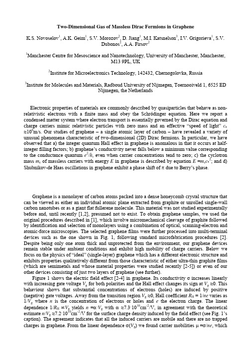
Two-Dimensional Gas of Massless Dirac Fermions in Graphene K.S. Novoselov1, A.K. Geim1, S.V. Morozov2, D. Jiang1, M.I. Katsnelson3, I.V. Grigorieva1, S.V. Dubonos2, A.A. Firsov21Manchester Centre for Mesoscience and Nanotechnology, University of Manchester, Manchester, M13 9PL, UK2Institute for Microelectronics Technology, 142432, Chernogolovka, Russia3Institute for Molecules and Materials, Radboud University of Nijmegen, Toernooiveld 1, 6525 ED Nijmegen, the NetherlandsElectronic properties of materials are commonly described by quasiparticles that behave as nonrelativistic electrons with a finite mass and obey the Schrödinger equation. Here we report a condensed matter system where electron transport is essentially governed by the Dirac equation and charge carriers mimic relativistic particles with zero mass and an effective “speed of light” c∗ ≈106m/s. Our studies of graphene – a single atomic layer of carbon – have revealed a variety of unusual phenomena characteristic of two-dimensional (2D) Dirac fermions. In particular, we have observed that a) the integer quantum Hall effect in graphene is anomalous in that it occurs at halfinteger filling factors; b) graphene’s conductivity never falls below a minimum value corresponding to the conductance quantum e2/h, even when carrier concentrations tend to zero; c) the cyclotron mass mc of massless carriers with energy E in graphene is described by equation E =mcc∗2; and d) Shubnikov-de Haas oscillations in graphene exhibit a phase shift of π due to Berry’s phase.Graphene is a monolayer of carbon atoms packed into a dense honeycomb crystal structure that can be viewed as either an individual atomic plane extracted from graphite or unrolled single-wall carbon nanotubes or as a giant flat fullerene molecule. This material was not studied experimentally before and, until recently [1,2], presumed not to exist. To obtain graphene samples, we used the original procedures described in [1], which involve micromechanical cleavage of graphite followed by identification and selection of monolayers using a combination of optical, scanning-electron and atomic-force microscopies. The selected graphene films were further processed into multi-terminal devices such as the one shown in Fig. 1, following standard microfabrication procedures [2]. Despite being only one atom thick and unprotected from the environment, our graphene devices remain stable under ambient conditions and exhibit high mobility of charge carriers. Below we focus on the physics of “ideal” (single-layer) graphene which has a different electronic structure and exhibits properties qualitatively different from those characteristic of either ultra-thin graphite films (which are semimetals and whose material properties were studied recently [2-5]) or even of our other devices consisting of just two layers of graphene (see further). Figure 1 shows the electric field effect [2-4] in graphene. Its conductivity σ increases linearly with increasing gate voltage Vg for both polarities and the Hall effect changes its sign at Vg ≈0. This behaviour shows that substantial concentrations of electrons (holes) are induced by positive (negative) gate voltages. Away from the transition region Vg ≈0, Hall coefficient RH = 1/ne varies as 1/Vg where n is the concentration of electrons or holes and e the electron charge. The linear dependence 1/RH ∝Vg yields n =α·Vg with α ≈7.3·1010cm-2/V, in agreement with the theoretical estimate n/Vg ≈7.2·1010cm-2/V for the surface charge density induced by the field effect (see Fig. 1’s caption). The agreement indicates that all the induced carriers are mobile and there are no trapped charges in graphene. From the linear dependence σ(Vg) we found carrier mobilities µ =σ/ne, whichreached up to 5,000 cm2/Vs for both electrons and holes, were independent of temperature T between 10 and 100K and probably still limited by defects in parent graphite. To characterise graphene further, we studied Shubnikov-de Haas oscillations (SdHO). Figure 2 shows examples of these oscillations for different magnetic fields B, gate voltages and temperatures. Unlike ultra-thin graphite [2], graphene exhibits only one set of SdHO for both electrons and holes. By using standard fan diagrams [2,3], we have determined the fundamental SdHO frequency BF for various Vg. The resulting dependence of BF as a function of n is plotted in Fig. 3a. Both carriers exhibit the same linear dependence BF = β·n with β ≈1.04·10-15 T·m2 (±2%). Theoretically, for any 2D system β is defined only by its degeneracy f so that BF =φ0n/f, where φ0 =4.14·10-15 T·m2 is the flux quantum. Comparison with the experiment yields f =4, in agreement with the double-spin and double-valley degeneracy expected for graphene [6,7] (cf. caption of Fig. 2). Note however an anomalous feature of SdHO in graphene, which is their phase. In contrast to conventional metals, graphene’s longitudinal resistance ρxx(B) exhibits maxima rather than minima at integer values of the Landau filling factor ν (Fig. 2a). Fig. 3b emphasizes this fact by comparing the phase of SdHO in graphene with that in a thin graphite film [2]. The origin of the “odd” phase is explained below. Another unusual feature of 2D transport in graphene clearly reveals itself in the T-dependence of SdHO (Fig. 2b). Indeed, with increasing T the oscillations at high Vg (high n) decay more rapidly. One can see that the last oscillation (Vg ≈100V) becomes practically invisible already at 80K whereas the first one (Vg <10V) clearly survives at 140K and, in fact, remains notable even at room temperature. To quantify this behaviour we measured the T-dependence of SdHO’s amplitude at various gate voltages and magnetic fields. The results could be fitted accurately (Fig. 3c) by the standard expression T/sinh(2π2kBTmc/heB), which yielded mc varying between ≈ 0.02 and 0.07m0 (m0 is the free electron mass). Changes in mc are well described by a square-root dependence mc ∝n1/2 (Fig. 3d). To explain the observed behaviour of mc, we refer to the semiclassical expressions BF = (h/2πe)S(E) and mc =(h2/2π)∂S(E)/∂E where S(E) =πk2 is the area in k-space of the orbits at the Fermi energy E(k) [8]. Combining these expressions with the experimentally-found dependences mc ∝n1/2 and BF =(h/4e)n it is straightforward to show that S must be proportional to E2 which yields E ∝k. Hence, the data in Fig. 3 unambiguously prove the linear dispersion E =hkc∗ for both electrons and holes with a common origin at E =0 [6,7]. Furthermore, the above equations also imply mc =E/c∗2 =(h2n/4πc∗2)1/2 and the best fit to our data yields c∗ ≈1⋅106 m/s, in agreement with band structure calculations [6,7]. The employed semiclassical model is fully justified by a recent theory for graphene [9], which shows that SdHO’s amplitude can indeed be described by the above expression T/sinh(2π2kBTmc/heB) with mc =E/c∗2. Note that, even though the linear spectrum of fermions in graphene (Fig. 3e) implies zero rest mass, their cyclotron mass is not zero. The unusual response of massless fermions to magnetic field is highlighted further by their behaviour in the high-field limit where SdHO evolve into the quantum Hall effect (QHE). Figure 4 shows Hall conductivity σxy of graphene plotted as a function of electron and hole concentrations in a constant field B. Pronounced QHE plateaux are clearly seen but, surprisingly, they do not occur in the expected sequence σxy =(4e2/h)N where N is integer. On the contrary, the plateaux correspond to half-integer ν so that the first plateau occurs at 2e2/h and the sequence is (4e2/h)(N + ½). Note that the transition from the lowest hole (ν =–½) to lowest electron (ν =+½) Landau level (LL) in graphene requires the same number of carriers (∆n =4B/φ0 ≈1.2·1012cm-2) as the transition between other nearest levels (cf. distances between minima in ρxx). This results in a ladder of equidistant steps in σxy which are not interrupted when passing through zero. To emphasize this highly unusual behaviour, Fig. 4 also shows σxy for a graphite film consisting of only two graphene layers where the sequence of plateaux returns to normal and the first plateau is at 4e2/h, as in the conventional QHE. We attribute this qualitative transition between graphene and its two-layer counterpart to the fact that fermions in the latter exhibit a finite mass near n ≈0 (as found experimentally; to be published elsewhere) and can no longer be described as massless Dirac particles. 2The half-integer QHE in graphene has recently been suggested by two theory groups [10,11], stimulated by our work on thin graphite films [2] but unaware of the present experiment. The effect is single-particle and intimately related to subtle properties of massless Dirac fermions, in particular, to the existence of both electron- and hole-like Landau states at exactly zero energy [912]. The latter can be viewed as a direct consequence of the Atiyah-Singer index theorem that plays an important role in quantum field theory and the theory of superstrings [13,14]. For the case of 2D massless Dirac fermions, the theorem guarantees the existence of Landau states at E=0 by relating the difference in the number of such states with opposite chiralities to the total flux through the system (note that magnetic field can also be inhomogeneous). To explain the half-integer QHE qualitatively, we invoke the formal expression [9-12] for the energy of massless relativistic fermions in quantized fields, EN =[2ehc∗2B(N +½ ±½)]1/2. In QED, sign ± describes two spins whereas in the case of graphene it refers to “pseudospins”. The latter have nothing to do with the real spin but are “built in” the Dirac-like spectrum of graphene, and their origin can be traced to the presence of two carbon sublattices. The above formula shows that the lowest LL (N =0) appears at E =0 (in agreement with the index theorem) and accommodates fermions with only one (minus) projection of the pseudospin. All other levels N ≥1 are occupied by fermions with both (±) pseudospins. This implies that for N =0 the degeneracy is half of that for any other N. Alternatively, one can say that all LL have the same “compound” degeneracy but zeroenergy LL is shared equally by electrons and holes. As a result the first Hall plateau occurs at half the normal filling and, oddly, both ν = –½ and +½ correspond to the same LL (N =0). All other levels have normal degeneracy 4B/φ0 and, therefore, remain shifted by the same ½ from the standard sequence. This explains the QHE at ν =N + ½ and, at the same time, the “odd” phase of SdHO (minima in ρxx correspond to plateaux in ρxy and, hence, occur at half-integer ν; see Figs. 2&3), in agreement with theory [9-12]. Note however that from another perspective the phase shift can be viewed as the direct manifestation of Berry’s phase acquired by Dirac fermions moving in magnetic field [15,16]. Finally, we return to zero-field behaviour and discuss another feature related to graphene’s relativistic-like spectrum. The spectrum implies vanishing concentrations of both carriers near the Dirac point E =0 (Fig. 3e), which suggests that low-T resistivity of the zero-gap semiconductor should diverge at Vg ≈0. However, neither of our devices showed such behaviour. On the contrary, in the transition region between holes and electrons graphene’s conductivity never falls below a well-defined value, practically independent of T between 4 and 100K. Fig. 1c plots values of the maximum resistivity ρmax(B =0) found in 15 different devices, which within an experimental error of ≈15% all exhibit ρmax ≈6.5kΩ, independent of their mobility that varies by a factor of 10. Given the quadruple degeneracy f, it is obvious to associate ρmax with h/fe2 =6.45kΩ where h/e2 is the resistance quantum. We emphasize that it is the resistivity (or conductivity) rather than resistance (or conductance), which is quantized in graphene (i.e., resistance R measured experimentally was not quantized but scaled in the usual manner as R =ρL/w with changing length L and width w of our devices). Thus, the effect is completely different from the conductance quantization observed previously in quantum transport experiments. However surprising, the minimum conductivity is an intrinsic property of electronic systems described by the Dirac equation [17-20]. It is due to the fact that, in the presence of disorder, localization effects in such systems are strongly suppressed and emerge only at exponentially large length scales. Assuming the absence of localization, the observed minimum conductivity can be explained qualitatively by invoking Mott’s argument [21] that mean-free-path l of charge carriers in a metal can never be shorter that their wavelength λF. Then, σ =neµ can be re-written as σ = (e2/h)kFl and, hence, σ cannot be smaller than ≈e2/h per each type of carriers. This argument is known to have failed for 2D systems with a parabolic spectrum where disorder leads to localization and eventually to insulating behaviour [17,18]. For the case of 2D Dirac fermions, no localization is expected [17-20] and, accordingly, Mott’s argument can be used. Although there is a broad theoretical consensus [18-23,10,11] that a 2D gas of Dirac fermions should exhibit a minimum 3conductivity of about e2/h, this quantization was not expected to be accurate and most theories suggest a value of ≈e2/πh, in disagreement with the experiment. In conclusion, graphene exhibits electronic properties distinctive for a 2D gas of particles described by the Dirac rather than Schrödinger equation. This 2D system is not only interesting in itself but also allows one to access – in a condensed matter experiment – the subtle and rich physics of quantum electrodynamics [24-27] and provides a bench-top setting for studies of phenomena relevant to cosmology and astrophysics [27,28].1. Novoselov, K.S. et al. PNAS 102, 10451 (2005). 2. Novoselov, K.S. et al. Science 306, 666 (2004); cond-mat/0505319. 3. Zhang, Y., Small, J.P., Amori, M.E.S. & Kim, P. Phys. Rev. Lett. 94, 176803 (2005). 4. Berger, C. et al. J. Phys. Chem. B, 108, 19912 (2004). 5. Bunch, J.S., Yaish, Y., Brink, M., Bolotin, K. & McEuen, P.L. Nanoletters 5, 287 (2005). 6. Dresselhaus, M.S. & Dresselhaus, G. Adv. Phys. 51, 1 (2002). 7. Brandt, N.B., Chudinov, S.M. & Ponomarev, Y.G. Semimetals 1: Graphite and Its Compounds (North-Holland, Amsterdam, 1988). 8. Vonsovsky, S.V. and Katsnelson, M.I. Quantum Solid State Physics (Springer, New York, 1989). 9. Gusynin, V.P. & Sharapov, S.G. Phys. Rev. B 71, 125124 (2005). 10. Gusynin, V.P. & Sharapov, S.G. cond-mat/0506575. 11. Peres, N.M.R., Guinea, F. & Castro Neto, A.H. cond-mat/0506709. 12. Zheng, Y. & Ando, T. Phys. Rev. B 65, 245420 (2002). 13. Kaku, M. Introduction to Superstrings (Springer, New York, 1988). 14. Nakahara, M. Geometry, Topology and Physics (IOP Publishing, Bristol, 1990). 15. Mikitik, G. P. & Sharlai, Yu.V. Phys. Rev. Lett. 82, 2147 (1999). 16. Luk’yanchuk, I.A. & Kopelevich, Y. Phys. Rev. Lett. 93, 166402 (2004). 17. Abrahams, E., Anderson, P.W., Licciardello, D.C. & Ramakrishnan, T.V. Phys. Rev. Lett. 42, 673 (1979). 18. Fradkin, E. Phys. Rev. B 33, 3263 (1986). 19. Lee, P.A. Phys. Rev. Lett. 71, 1887 (1993). 20. Ziegler, K. Phys. Rev. Lett. 80, 3113 (1998). 21. Mott, N.F. & Davis, E.A. Electron Processes in Non-Crystalline Materials (Clarendon Press, Oxford, 1979). 22. Morita, Y. & Hatsugai, Y. Phys. Rev. Lett. 79, 3728 (1997). 23. Nersesyan, A.A., Tsvelik, A.M. & Wenger, F. Phys. Rev. Lett. 72, 2628 (1997). 24. Rose, M.E. Relativistic Electron Theory (John Wiley, New York, 1961). 25. Berestetskii, V.B., Lifshitz, E.M. & Pitaevskii, L.P. Relativistic Quantum Theory (Pergamon Press, Oxford, 1971). 26. Lai, D. Rev. Mod. Phys. 73, 629 (2001). 27. Fradkin, E. Field Theories of Condensed Matter Systems (Westview Press, Oxford, 1997). 28. Volovik, G.E. The Universe in a Helium Droplet (Clarendon Press, Oxford, 2003).Acknowledgements This research was supported by the EPSRC (UK). We are most grateful to L. Glazman, V. Falko, S. Sharapov and A. Castro Netto for helpful discussions. K.S.N. was supported by Leverhulme Trust. S.V.M., S.V.D. and A.A.F. acknowledge support from the Russian Academy of Science and INTAS.43µ (m2/Vs)0.8c4P0.4 22 σ (1/kΩ)10K0 0 1/RH(T/kΩ) 1 2ρmax (h/4e2)1-5010 Vg (V) 50 -10ab 0 -100-500 Vg (V)50100Figure 1. Electric field effect in graphene. a, Scanning electron microscope image of one of our experimental devices (width of the central wire is 0.2µm). False colours are chosen to match real colours as seen in an optical microscope for larger areas of the same materials. Changes in graphene’s conductivity σ (main panel) and Hall coefficient RH (b) as a function of gate voltage Vg. σ and RH were measured in magnetic fields B =0 and 2T, respectively. The induced carrier concentrations n are described by [2] n/Vg =ε0ε/te where ε0 and ε are permittivities of free space and SiO2, respectively, and t ≈300 nm is the thickness of SiO2 on top of the Si wafer used as a substrate. RH = 1/ne is inverted to emphasize the linear dependence n ∝Vg. 1/RH diverges at small n because the Hall effect changes its sign around Vg =0 indicating a transition between electrons and holes. Note that the transition region (RH ≈ 0) was often shifted from zero Vg due to chemical doping [2] but annealing of our devices in vacuum normally allowed us to eliminate the shift. The extrapolation of the linear slopes σ(Vg) for electrons and holes results in their intersection at a value of σ indistinguishable from zero. c, Maximum values of resistivity ρ =1/σ (circles) exhibited by devices with different mobilites µ (left y-axis). The histogram (orange background) shows the number P of devices exhibiting ρmax within 10% intervals around the average value of ≈h/4e2. Several of the devices shown were made from 2 or 3 layers of graphene indicating that the quantized minimum conductivity is a robust effect and does not require “ideal” graphene.ρxx (kΩ)0.60 aVg = -60V4B (T)810K12∆σxx (1/kΩ)0.4 1ν=4 140K 80K B =12T0 b 0 25 50 Vg (V) 7520K100Figure 2. Quantum oscillations in graphene. SdHO at constant gate voltage Vg as a function of magnetic field B (a) and at constant B as a function of Vg (b). Because µ does not change much with Vg, the constant-B measurements (at a constant ωcτ =µB) were found more informative. Panel b illustrates that SdHO in graphene are more sensitive to T at high carrier concentrations. The ∆σxx-curves were obtained by subtracting a smooth (nearly linear) increase in σ with increasing Vg and are shifted for clarity. SdHO periodicity ∆Vg in a constant B is determined by the density of states at each Landau level (α∆Vg = fB/φ0) which for the observed periodicity of ≈15.8V at B =12T yields a quadruple degeneracy. Arrows in a indicate integer ν (e.g., ν =4 corresponds to 10.9T) as found from SdHO frequency BF ≈43.5T. Note the absence of any significant contribution of universal conductance fluctuations (see also Fig. 1) and weak localization magnetoresistance, which are normally intrinsic for 2D materials with so high resistivity.75 BF (T) 500.2 0.11/B (1/T)b5 10 N 1/2025 a 0 0.061dmc /m00.04∆0.02 0c0 0 T (K) 150n =0e-6-3036Figure 3. Dirac fermions of graphene. a, Dependence of BF on carrier concentration n (positive n correspond to electrons; negative to holes). b, Examples of fan diagrams used in our analysis [2] to find BF. N is the number associated with different minima of oscillations. Lower and upper curves are for graphene (sample of Fig. 2a) and a 5-nm-thick film of graphite with a similar value of BF, respectively. Note that the curves extrapolate to different origins; namely, to N = ½ and 0. In graphene, curves for all n extrapolate to N = ½ (cf. [2]). This indicates a phase shift of π with respect to the conventional Landau quantization in metals. The shift is due to Berry’s phase [9,15]. c, Examples of the behaviour of SdHO amplitude ∆ (symbols) as a function of T for mc ≈0.069 and 0.023m0; solid curves are best fits. d, Cyclotron mass mc of electrons and holes as a function of their concentration. Symbols are experimental data, solid curves the best fit to theory. e, Electronic spectrum of graphene, as inferred experimentally and in agreement with theory. This is the spectrum of a zero-gap 2D semiconductor that describes massless Dirac fermions with c∗ 300 times less than the speed of light.n (1012 cm-2)σxy (4e2/h)4 3 2 -2 1 -1 -2 -3 2 44Kn7/ 5/ 3/ 1/2 2 2 210 ρxx (kΩ)-4σxy (4e2/h)0-1/2 -3/2 -5/2514T0-7/2 -4 -2 0 2 4 n (1012 cm-2)Figure 4. Quantum Hall effect for massless Dirac fermions. Hall conductivity σxy and longitudinal resistivity ρxx of graphene as a function of their concentration at B =14T. σxy =(4e2/h)ν is calculated from the measured dependences of ρxy(Vg) and ρxx(Vg) as σxy = ρxy/(ρxy + ρxx)2. The behaviour of 1/ρxy is similar but exhibits a discontinuity at Vg ≈0, which is avoided by plotting σxy. Inset: σxy in “two-layer graphene” where the quantization sequence is normal and occurs at integer ν. The latter shows that the half-integer QHE is exclusive to “ideal” graphene.。

“Graphene”研究及翻译摘要:查阅近5年我国SCI、EI期源刊有关石墨烯研究873篇,石墨烯研究的有关翻译存在很大差异。
从石墨烯的发现史及简介,谈石墨烯内涵及研究的相关翻译。
指出“石墨烯”有关术语翻译、英文题目、摘要撰写应注意的问题。
关键词:石墨烯;石墨烯术语;翻译石墨烯是目前发现的唯一存在的二维自由态原子晶体,它是构筑零维富勒烯、一维碳纳米管、三维体相石墨等sp2杂化碳的基本结构单元,具有很多奇异的电子及机械性能。
因而吸引了化学、材料等其他领域科学家的高度关注。
近5年我国SCI、EI期源刊研究论文873篇,论文质量良莠不齐,发表的论文有35.97%尚未被引用过,占国际论文被引的4.84%左右。
石墨烯研究的有关翻译也存在很大差异。
为了更好的进行国际学术交流,规范化专业术语。
本文就“graphene”的内涵及翻译谈以下看法。
l “Graphene”的发现史及简介1962年,Boehm等人在电镜上观察到了数层甚至单层石墨(氧化物)的存在,1975年van Bom-mel等人报道少层石墨片的外延生长研究,1999年德克萨斯大学奥斯汀分校的R Ruoff等人对用透明胶带从块体石墨剥离薄层石墨片的尝试进行相关报道。
2004年曼彻斯特大学的Novoselov和Geim小组以石墨为原料,通过微机械力剥离法得到一系列叫作二维原子晶体的新材料——石墨烯,并于10月22日在Sclence期刊上发表有关少层乃至单层石墨片的独特电学性质的文章,2010年Gelm和No-voselov获得了诺贝尔物理学奖。
石墨烯有着巨大的比表面积(2630 m2/g)、极高的杨氏模量(1.06 TPa)和断裂应力(~130GPa)、超高电导率(~106 S/cm)和热导率(5000W/m·K)。
石墨烯中的载流子迁移率远高于传统的硅材料,室温下载流子的本征迁移率高达200000 cm2/V.s),而典型的硅场效应晶体管的电子迁移率仅约1000 cm2/V.s。

曹原石墨烯英语介绍Graphene: The Extraordinary Material Discovered by Cao YuanGraphene, a remarkable material discovered by Cao Yuan, has captivated the scientific community and captured the imagination of the public. This single-atom-thick layer of carbon has revolutionized various fields, from electronics and energy storage to materials science and biomedicine. In this comprehensive introduction, we will delve into the fascinating properties, applications, and the story behind the discovery of this transformative material.Cao Yuan's Groundbreaking DiscoveryCao Yuan, a Chinese physicist, and his research team at the University of Manchester made a groundbreaking discovery in 2004 when they successfully isolated and characterized graphene. This achievement was the culmination of years of research and experimentation, and it earned Cao Yuan and his colleagues the Nobel Prize in Physics in 2010.The path to the discovery of graphene was not an easy one. Researchers had long theorized about the existence of a two-dimensional material composed of carbon atoms, but its realizationhad been considered impossible due to the inherent instability of such a structure. Cao Yuan and his team, however, persevered and developed a simple yet ingenious method to extract graphene from graphite, the material found in pencils.The Remarkable Properties of GrapheneGraphene's unique atomic structure, with its tightly packed carbon atoms arranged in a hexagonal lattice, gives rise to a remarkable set of properties that have captured the attention of scientists and engineers worldwide. One of the most striking characteristics of graphene is its extraordinary strength, with a tensile strength 200 times greater than that of steel. This makes it an ideal candidate for applications that require durable and lightweight materials, such as in the aerospace and automotive industries.In addition to its remarkable strength, graphene is also an exceptional conductor of electricity and heat. Its high electrical conductivity allows for the development of faster and more efficient electronic devices, while its thermal conductivity makes it a valuable material for heat dissipation in electronic systems. These properties have led to the exploration of graphene in a wide range of applications, from transparent and flexible electronics to energy storage devices and sensors.Graphene's Potential ApplicationsThe discovery of graphene has opened up a world of possibilities, and researchers are actively exploring its potential applications in various fields. In the realm of electronics, graphene's unique properties have enabled the development of high-speed transistors, flexible displays, and advanced sensors. The material's transparency and conductivity make it an ideal candidate for use in touch screens and flexible electronics, potentially leading to the creation of foldable smartphones and wearable devices.In the field of energy, graphene's exceptional performance as an electrode material has led to the development of advanced batteries and supercapacitors. These energy storage devices have the potential to revolutionize the way we power our devices and vehicles, offering faster charging times, higher energy density, and longer lifespans.Moreover, graphene's potential in the biomedical field is equally promising. Researchers are exploring the use of graphene in drug delivery systems, tissue engineering, and biosensors. The material's biocompatibility and ability to interact with biological systems make it a promising candidate for various medical applications, from targeted cancer therapies to neural interfaces.The Ongoing Exploration of GrapheneAs the scientific community continues to delve deeper into the worldof graphene, new and exciting discoveries are being made. Researchers are constantly exploring ways to optimize the production and processing of graphene, as well as investigating its interactions with other materials to create novel composite structures.One area of particular interest is the development of graphene-based composites, which combine the exceptional properties of graphene with other materials to create even more versatile and functional materials. These composite materials have the potential to revolutionize industries ranging from construction to aerospace, offering enhanced strength, durability, and functionality.Furthermore, the exploration of graphene's potential in the realm of quantum computing and spintronics is an active area of research. The material's unique electronic properties, such as its high electron mobility and the ability to control the spin of electrons, could pave the way for the development of next-generation computing and information processing technologies.ConclusionCao Yuan's discovery of graphene has undoubtedly been a transformative moment in the history of materials science. This remarkable material has opened up a world of possibilities, with its exceptional properties and diverse applications capturing theimagination of scientists, engineers, and the general public alike.As the exploration of graphene continues, we can expect to see even more groundbreaking advancements in fields ranging from electronics and energy to biomedicine and beyond. The potential of this material to revolutionize our world is truly limitless, and the story of its discovery is a testament to the power of human ingenuity and the relentless pursuit of scientific knowledge.。
《基于石墨烯光子晶体光纤的流体传感器(英文)》篇一Based on Graphene Photonic Crystal Fiber Fluid SensorsAbstract:This paper presents a novel fluid sensor based on graphene photonic crystal fiber technology. The sensor utilizes the unique properties of graphene and photonic crystal fibers to achieve high sensitivity and accuracy in fluid detection. The structure and function of the proposed sensor are described, along with its advantages and potential applications in various fields.I. IntroductionWith the rapid development of modern technology, sensors have become increasingly important in various fields, including industrial, medical, and environmental monitoring. Among various types of sensors, fluid sensors play a crucial role in monitoring the quality and quantity of fluids. Graphene, a material with excellent electrical and optical properties, has recently gained widespread attention in the field of sensor development. This paper proposes a new type of fluid sensor based on graphene photonic crystal fiber technology, which can provide accurate and real-time fluid detection with high sensitivity and durability.II. BackgroundGraphene is a two-dimensional material consisting of a single layer of carbon atoms arranged in a honeycomb lattice. Due to its unique electrical and optical properties, graphene has been widely usedin various fields such as electronics, optics, and sensors. Photonic crystal fibers are optical fibers that can control the propagation of light at the microscale level. They have been widely used in high-precision sensing applications. By combining the advantages of graphene and photonic crystal fibers, we can develop a new type of fluid sensor that is more sensitive and accurate.III. Proposed Sensor Structure and FunctionThe proposed fluid sensor is based on graphene photonic crystal fiber technology. The sensor consists of a graphene-coated photonic crystal fiber, which is immersed in the fluid to be measured. When the fluid flows through the sensor, it interacts with the graphene-coated photonic crystal fiber, resulting in changes in the propagation of light within the fiber. These changes can be detected and measured by an optical detection system, providing accurate and real-time fluid detection information.The graphene coating enhances the sensitivity of the sensor by improving the interaction between the fluid and the photonic crystal fiber. Additionally, the two-dimensional structure of graphene allows for more efficient light absorption and transmission, further improving the performance of the sensor. The photonic crystal fiber provides precise control of light propagation, ensuring accurate detection of fluid properties such as concentration, temperature, and pressure.IV. Advantages and ApplicationsThe proposed fluid sensor based on graphene photonic crystal fiber technology has several advantages compared to traditional fluid sensors. Firstly, it has high sensitivity and accuracy, which can detecteven small changes in fluid properties. Secondly, it has excellent durability and stability, ensuring long-term reliable performance. Thirdly, it is easy to fabricate and integrate with other components, making it suitable for mass production and application in various fields.The proposed fluid sensor can be widely used in industrial, medical, environmental monitoring, and other fields. For example, it can be used to monitor the quality of water in industrial processes or drinking water systems, detect chemicals or biological substances in laboratory experiments or medical treatments, or monitor environmental pollutants in real-time.V. ConclusionIn conclusion, this paper presents a novel fluid sensor based on graphene photonic crystal fiber technology. The proposed sensor utilizes the unique properties of graphene and photonic crystal fibers to achieve high sensitivity and accuracy in fluid detection. The advantages of this new type of sensor include high sensitivity, excellent durability, easy fabrication and integration, and wide application fields. With further research and development, this type of fluid sensor has great potential to improve the performance of various industries and fields.The potential of this new fluid sensor is not limited to the fields mentioned above. With the continuous development of technology and the increasing demand for high-precision fluid detection, this type of sensor will play an increasingly important role in various fields. It can be used to improve the efficiency and accuracy of industrial production processes, enhance medical treatment quality, and protect the environment by monitoringpollutants in real-time. In addition, this type of sensor can also be applied in the field of smart homes, providing accurate and timely information on water quality and air quality, ensuring a healthy and comfortable living environment.In summary, the proposed fluid sensor based on graphene photonic crystal fiber technology offers a new approach to fluid detection with high sensitivity, accuracy, and durability. Its wide range of applications and potential to improve various industries and fields make it a promising research direction in the future.。
ARTICLEReceived1Apr2014|Accepted9Jan2015|Published24Feb2015Observation of long-lived interlayer excitonsin monolayer MoSe2–WSe2heterostructuresPasqual Rivera1,John R.Schaibley1,Aaron M.Jones1,Jason S.Ross2,Sanfeng Wu1,Grant Aivazian1,Philip Klement1,Kyle Seyler1,Genevieve Clark2,Nirmal J.Ghimire3,4,Jiaqiang Yan4,5,D.G.Mandrus3,4,5, Wang Yao6&Xiaodong Xu1,2Van der Waals bound heterostructures constructed with two-dimensional materials,such asgraphene,boron nitride and transition metal dichalcogenides,have sparked wide interest indevice physics and technologies at the two-dimensional limit.One highly coveted hetero-structure is that of differing monolayer transition metal dichalcogenides with type-II bandalignment,with bound electrons and holes localized in individual monolayers,that is,interlayer excitons.Here,we report the observation of interlayer excitons in monolayerMoSe2–WSe2heterostructures by photoluminescence and photoluminescence excitationspectroscopy.Wefind that their energy and luminescence intensity are highly tunable by anapplied vertical gate voltage.Moreover,we measure an interlayer exciton lifetime of B1.8ns,an order of magnitude longer than intralayer excitons in monolayers.Our work demonstratesoptical pumping of interlayer electric polarization,which may provoke further explorationof interlayer exciton condensation,as well as new applications in two-dimensional lasers,light-emitting diodes and photovoltaic devices.1Department of Physics,University of Washington,Seattle,Washington98195,USA.2Department of Materials Science and Engineering,University of Washington,Seattle,Washington98195,USA.3Department of Physics and Astronomy,University of T ennessee,Knoxville,T ennessee37996,USA.4Materials Science and T echnology Division,Oak Ridge National Laboratory,Oak Ridge,T ennessee37831,USA.5Department of Materials Science and Engineering,University of T ennessee,Knoxville,T ennessee37996,USA.6Department of Physics and Center of Theoretical and Computational Physics, University of Hong Kong,Hong Kong,China.Correspondence and requests for materials should be addressed to P.R.(email:pasqual@)or to X.X. (email:xuxd@).T he recently developed ability to vertically assemble different two-dimensional(2D)materials heralds a newrealm of device physics based on van der Waals heterostructures(HSs)1.The most successful example to date is the vertical integration of graphene on boron nitride.Such novel HSs not only markedly enhance graphene’s electronic properties2, but also give rise to superlattice structures demonstrating exotic physical phenomena3–5.A fascinating counterpart to gapless graphene is a class of monolayer direct bandgap semiconductors, namely transition metal dichalcogenides(TMDs)6–8.Due to the large binding energy in these2D semiconductors,excitons dominate the optical response,exhibiting strong light–matter interactions that are electrically tunable9,10.The discovery of excitonic valley physics11–15and strongly coupled spin and pseudospin physics16,17in2D TMDs opens up new possibilities for device concepts not possible in other material systems. Monolayer TMDs have the chemical formula MX2where the M is tungsten(W)or molybdenum(Mo),and the X is sulfur(S) or selenium(Se).Although these TMDs share the same crystalline structure,their physical properties,such as bandgap,exciton resonance and spin–orbit coupling strength,can vary signifi-cantly.Therefore,an intriguing possibility is to stack different TMD monolayers on top of one another to form2D HSs.First-principle calculations show that heterojunctions formed between monolayer tungsten and molybdenum dichalcogenides have type-II band alignment18–20.Recently,this has been confirmed by X-ray photoelectron spectroscopy and scanning tunnelling spectroscopy21.Since the Coulomb binding energy in2D TMDs is much stronger than in conventional semiconductors, it is possible to realize interlayer excitonic states in van der Waals bound heterobilayers,that is,bound electrons and holes that are localized in different layers.Such interlayer excitons have been intensely pursued in bilayer graphene for possible exciton condensation22,but direct optical observation demonstrating the existence of such excitons is challenging owing to the lack of a sizable bandgap in graphene.Monolayer TMDs with bandgaps in the visible range provide the opportunity to optically pump interlayer excitons,which can be directly observed through photoluminescence(PL)measurements.In this report,we present direct observation of interlayer excitons in vertically stacked monolayer MoSe2–WSe2HSs.We show that interlayer exciton PL is enhanced under optical excitation resonant with the intralayer excitons in isolated monolayers,consistent with the interlayer charge transfer resulting from the underlying type-II band structure.We demonstrate the tuning of the interlayer exciton energy by applying a vertical gate voltage,which is consistent with the permanent out-of-plane electric dipole nature of interlayer excitons.Moreover,wefind a blue shift in PL energy at increasing excitation power,a hallmark of repulsive dipole–dipole interac-tions between spatially indirect excitons.Finally,time-resolved PL measurements yield a lifetime of1.8ns,which is at least an order of magnitude longer than that of intralayer excitons.Our work shows that monolayer semiconducting HSs are a promising platform for exploring new optoelectronic phenomena.ResultsMoSe2–WSe2HS photoluminescence.HSs are prepared by standard polymethyl methacrylate(PMMA)transfer techniques using mechanically exfoliated monolayers of WSe2and MoSe2(see Methods).Since there is no effort made to match the crystal lattices of the two monolayers,the obtained HSs are considered incom-mensurate.An idealized depiction of the vertical MoSe2–WSe2HS is shown in Fig.1a.We have fabricated six devices that all show similar results as those reported below.The data presented here are from two independent MoSe2–WSe2HSs,labelled device1and device2.Figure1b shows an optical micrograph of device1,which has individual monolayers,as well as a large area of vertically stacked HS.This device architecture allows for the comparison of the excitonic spectrum of individual monolayers with that of the HS region,allowing for a controlled identification of spectral changes resulting from interlayer coupling.We characterize the MoSe2–WSe2monolayers and HS using PL measurements.Inspection of the PL from the HS at room temperature reveals three dominant spectral features(Fig.1c). The emission at1.65and1.57eV corresponds to the excitonic states from monolayer WSe2and MoSe2(refs10,15),respectively. PL from the HS region,outlined by the dashed white line in Fig.1a,reveals a distinct spectral feature at1.35eV(X I).Two-dimensional mapping of the spectrally integrated PL from X I shows that it is isolated entirely to the HS region(inset,Fig.1c), with highly uniform peak intensity and spectral position (Supplementary Materials1).Low-temperature characterization of the HS is performed with 1.88eV laser excitation at20K.PL from individual monolayer WSe2(top),MoSe2(bottom)and the HS area(middle)are shown with the same scale in Fig.1d.At low temperature,the intralayer neutral(X M o)and charged(X MÀ)excitons are resolved10,15,where M labels either W or parison of the three spectra shows that both intralayer X M o and X MÀexist in the HS with emission at the same energy as from isolated monolayers,demonstrating the preservation of intralayer excitons in the HS region.PL from X I becomes more pronounced and is comparable to the intralayer excitons at low temperature.We note that the X I energy position has variation across the pool of HS samples we have studied (Supplementary Fig.1),which we attribute to differences in the interlayer separation,possibly due to imperfect transfer and a different twisting angle between monolayers.We further perform PL excitation(PLE)spectroscopy to investigate the correlation between X I and intralayer excitons.A narrow bandwidth(o50kHz)frequency tunable laser is swept across the energy resonances of intralayer excitons(from1.6to 1.75eV)while monitoring X I PL response.Figure2a shows an intensity plot of X I emission as a function of photoexcitation energy from device2.We clearly observe the enhancement of X I emission when the excitation energy is resonant with intralayer exciton states(Fig.2b).Now we discuss the origin of X I.Since X I has never been observed in our exfoliated monolayer and bilayer samples,if its origin were related to defects,they must be introduced by the fabrication process.This would result in sample-dependent X I properties with non-uniform spatial dependence.However,our data show that key physical properties of X I,such as the resonance energy and intensity,are spatially uniform and isolated to the HS region(inset of Fig.1c and Supplementary Fig.2).In addition,X I has not been observed in WSe2–WSe2homo-structures constructed from exfoliated or physical vapor deposi-tion(PVD)grown monolayers(Supplementary Fig.3).All these facts suggest that X I is not a defect-related exciton.Instead,the experimental results support the observation of an interlayer exciton.Due to the type-II band alignment of the MoSe2–WSe2HS18–20,as shown in Fig.2c,photoexcited electrons and holes will relax(dashed lines)to the conduction band edge of MoSe2and the valence band edge of WSe2,respectively.The Coulomb attraction between electrons in the MoSe2and holes in the WSe2gives rise to an interlayer exciton,X I,analogous to spatially indirect excitons in coupled quantum wells.The interlayer coupling yields the lowest energy bright exciton in the HS,which is consistent with the temperature dependence of X I PL,that is,it increases as temperature decreases (Supplementary Fig.4).From the intralayer and interlayer exciton spectral positions,we can infer the band offsets between the WSe 2and MoSe 2monolayers (Fig.2c).The energy difference between X W and X I at room temperature is 310meV.Considering the smaller binding energy of interlayer than intralayer excitons,this sets a lower bound on the conduction band offset.The energy difference between X M and X I then provides a lower bound on the valence band offset of 230meV.This value is consistent with the valence band offset of 228meV found in MoS 2–WSe 2HSs by micro X-ray photoelectron spectroscopy and scanning tunnelling spectro-scopy measurements 21.This experimental evidence strongly corroborates X I as an interlayer exciton.The observation of bright interlayer excitons in monolayer semiconducting HSs is of central importance,and the remainder of this paper will focus on their physical properties resulting from their spatially indirect nature and the underlying type-II band alignment.WSe 2HSMoSe 2W M SeIn te n s i t y (a .u .)1.31.51.7Energy (eV)MoSe 2HeterostructureWSe 2W0WX X X X −0MoMo−e hehe h1.3 1.41.51.6 1.7I n t e n s i t y (a .u .)Energy (eV)5μm 0123×104Y (μm )246X (μm)0246Figure 1|Intralayer and interlayer excitons of a monolayer MoSe 2–WSe 2vertical heterostructure.(a )Cartoon depiction of a MoSe 2–WSe 2heterostructure (HS).(b )Microscope image of a MoSe 2–WSe 2HS (device 1)with a white dashed line outlining the HS region.(c )Room-temperature photoluminescence of the heterostructure under 20m W laser excitation at 2.33eV.Inset:spatial map of integrated PL intensity from the low-energy peak (1.273–1.400eV),which is only appreciable in the heterostructure area,outlined by the dashed black line.(d )Photoluminescence of individual monolayers and the HS at 20K under 20m W excitation at 1.88eV (plotted on the samescale).Energy (eV)WSe MoSe PL energy (eV)E x c i t a t i o n e n e r g y (e V )1.28 1.3 1.32 1.34 1.36 1.381.61.651.71.754,0006,0008,00010,000IntensityFigure 2|Photoluminescence excitation spectroscopy of the interlayer exciton at 20K.(a )PLE intensity plot of the heterostructure region with an excitation power of 30m W and 5s charge-coupled device CCD integration time.(b )Spectrally integrated PLE response (red dots)overlaid on PL (black line)with 100m W excitation at 1.88eV.(c )Type-II semiconductor band alignment diagram for the 2D MoSe 2–WSe 2heterojunction.interlayer exciton .Applying vertical energy of Figure 3a contact stacked insu-Electrostatic contact shows the 100to about analogue of reversed,varied expected for from reduces device 2,conduction 3b,c.of the in the on top band-offset at X I PL energy of basis of would should have X I PL This effect,intensity.further Power dependence and lifetime of interlayer exciton PL .The interlayer exciton PLE spectrum as a function of laser power with excitation energy in resonance with X W o reveals several properties of the X I .Inspection of the normalized PLE intensity (Fig.4a)shows the evolution of a doublet in the interlayer excitonspectrum,highlighted by the red and Both peaks of the doublet display a consistent increased laser intensity,shown by the dashed which are included as a guide to the eye.intensity of X I also exhibits a strong saturation laser power,as shown in Fig.4b (absolute Supplementary Fig.6).The sublinear power excitation powers above 0.5m W is distinctly the intralayer excitons in isolated monolayers,saturation power threshold of about Fig.7).The low power saturation of X I PL lifetime than that of intralayer excitons.the intralayer exciton is substantially reduced interlayer charge hopping 23,which is quenching of intralayer exciton PL (Fig.Fig.8).Moreover,the lifetime of the interlayer because it is the lowest energy configuration indirect nature leads to a reduced optical long lifetime is confirmed by time-resolved Fig.4c.A fit to a single exponential decay exciton lifetime of 1.8±0.3ns.This timescale the intralayer exciton lifetime,which is ps 24–27.By modelling the saturation behaviour three-level diagram,the calculated saturation interlayer exciton is about 180times (Supplementary Fig.7;Supplementary with our observation of low saturation intensity DiscussionWe attribute the observed doublet feature splitting of the monolayer MoSe 2conduction assignment is mainly based on the fact difference between the doublet is B 25with MoSe 2conduction band splitting predicted calculations 28.This explanation is also supported by the evolution of the relative strength of the two peaks with increasing excitation power,as shown in Fig.4a (similar results in device 1with 1.88eV excitation shown in Supplementary Fig.9).At low power,the lowest energy configuration of interlayer excitons,with the electron in the lower spin-split band of MoSe 2,is populated first.Due to phase space filling effects,the interlayer excitonSiO 2n + Si2MoSe 2e –h +e –h +P Ee –h +V g < 0WSe 2MoSe 2WSe 2MoSe 2h ωV g = 0Photon energy (eV)1.321.361.41.444080e –h +h +PL intensity (a.u.) -hω’-the interlayer exciton and band alignment.(a )Device 2geometry.The interlayer exciton has a out-of-plane electric polarization.(b )Electrostatic control of the band alignment and the interlayer exciton photoluminescence as a function of applied gate voltage under 70m W excitation at 1.744eV,1s integrationconfiguration with the electron in the higher energy spin-split band starts to be filled at higher laser power.Consequently,the higher energy peak of the doublet becomes more prominent at higher excitation powers.The observed blue shift of X I as the excitation power increases,indicated by the dashed arrows in Fig.4a,is a signature of the repulsive interaction between the dipole-aligned interlayer excitons (cf.Fig.3a).This is a hallmark of spatially indirect excitons in gallium arsenide (GaAs)coupled quantum wells,which have been intensely studied for exciton Bose-Einstein condensation (BEC)phenomena 29.The observation of spatially indirect interlayer excitons in a type-II semiconducting 2D HS provides an intriguing platform to explore exciton BEC,where the observed extended lifetimes and repulsive interactions are two key ingredients towards the realization of this exotic state of matter.Moreover,the extraordinarily high binding energy for excitons in this truly 2D system may provide for degenerate exciton gases at elevated temperatures compared with other material systems 30.The long-lived interlayer exciton may also lead to new optoelectronic applications,such as photovoltaics 31–34and 2D HS nanolasers.MethodsDevice fabrication .Monolayers of MoSe 2are mechanically exfoliated onto 300nm SiO 2on heavily doped Si wafers and monolayers of WSe 2onto a layer of PMMA atop polyvinyl alcohol on Si.Both monolayers are identified with an opticalmicroscope and confirmed by their PL spectra.Polyvinyl alcohol is dissolved in H 2O and the PMMA layer is then placed on a transfer loop or thin layer of poly-dimethylsiloxane (PDMS).The top monolayer is then placed in contact with the bottom monolayer with the aid of an optical microscope and micromanipulators.The substrate is then heated to cause the PMMA layer to release from the transfer media.The PMMA is subsequently dissolved in acetone for B 30min and then rinsed with isopropyl alcohol.Low-temperature PL measurements .Low-temperature measurements are con-ducted in a temperature-controlled Janis cold finger cryostat (sample in vacuum)with a diffraction-limited excitation beam diameter of B 1m m.PL is spectrally filtered through a 0.5-m monochromator (Andor–Shamrock)and detected on a charge-coupled device (Andor—Newton).Spatial PL mapping is performed using a Mad City Labs Nano-T555nanopositioning system.For PLE measurements,a continuous wave Ti:sapphire laser (MSquared—SolsTiS)is used for excitation and filtered from the PL signal using an 815-nm-long pass optical filter (Semrock).Electrostatic doping is accomplished with an indium drain contact deposited onto the monolayer WSe 2region of device 2and using the heavily doped Si as a tunable backgate.Time-resolved PL measurements .For interlayer lifetime measurements,we excite the sample with a o 200-fs pulsed Ti:sapphire laser (Coherent—MIRA).Interlayer PL is spectrally filtered through a 0.5-m monochromator (Princeton—Acton 2500),and detected with a fast time-correlated single-photon counting system composed of a fast (o 30ps full width at half maximum)single-photon avalanche detector (Micro Photon Devices—PDM series)and a picosecond event timer (PicoQuant—PicoHarp 300).References1.Geim,A.K.&Grigorieva,I.V.Van der Waals heterostructures.Nature 499,419–425(2013).2.Dean,C.R.et al.Boron nitride substrates for high-quality graphene electronics.Nat.Nanotechnol.5,722–726(2010).3.Hunt,B.et al.Massive Dirac fermions and Hofstadter butterfly in a van derWaals heterostructure.Science 340,1427–1430(2013).4.Dean,C.R.et al.Hofstadter’s butterfly and the fractal quantum Hall effect inmoire superlattices.Nature 497,598–602(2013).5.Ponomarenko,L.A.et al.Cloning of Dirac fermions in graphene superlattices.Nature 497,594–597(2013).6.Novoselov,K.S.et al.Two-dimensional atomic crystals.Proc.Natl Acad.SciUSA 102,10451–10453(2005).7.Mak,K.F.,Lee,C.,Hone,J.,Shan,J.&Heinz,T.F.Atomically thin MoS 2:anew direct-gap semiconductor.Phys.Rev.Lett.105,136805(2010).8.Splendiani,A.et al.Emerging photoluminescence in monolayer MoS 2.NanoLett.10,1271–1275(2010).MoSe2WSe 2dPhoton energy (eV)Laser power (μW)Time (ns)I n t e n s i t y (a .u .)N o r m a l i z e d P L E i n t e n s i t y (c o u n t s (μW s )–1)Power (μW)I n t e g r a t e d P L E i n t e n s i t y (C o u n t s (μW s )–1)2060404Figure 4|Power-dependent photoluminescence of interlayer exciton and its lifetime at 20K.(a )Power dependence of the interlayer exciton for 1.722eV excitation with a bi-Lorentzian fit to the 5and 100m W plots,normalized for power and charge-coupled device (CCD)integration time.(b )Spectrally integrated intensity of the interlayer exciton emission as a function of excitation power shows the saturation effect.(c )Time-resolvedphotoluminescence of the interlayer exciton (1.35eV)shows a lifetime of about 1.8ns.The dashed curve is the instrument response to the excitation laser pulse.(d )Illustration of the heterojunction band diagram,including the spin levels of the MoSe 2conduction band.The X I doublet has energy splitting equal to (o 0I Ào I )E 25meV.9.Mak,K.F.et al.Tightly bound trions in monolayer MoS2.Nat.Mater.12,207–211(2013).10.Ross,J.S.et al.Electrical control of neutral and charged excitons in amonolayer mun.4,1474(2013).11.Xiao,D.,Liu,G.-B.,Feng,W.,Xu,X.&Yao,W.Coupled spin and valleyphysics in monolayers of MoS2and other group-VI dichalcogenides.Phys.Rev.Lett.108,196802(2012).12.Cao,T.et al.Valley-selective circular dichroism of monolayer molybdenummun.3,887(2012).13.Zeng,H.,Dai,J.,Yao,W.,Xiao,D.&Cui,X.Valley polarization inMoS2monolayers by optical pumping.Nat.Nanotechnol.7,490–493(2012).14.Mak,K.F.,He,K.,Shan,J.&Heinz,T.F.Control of valley polarization inmonolayer MoS2by optical helicity.Nat.Nanotechnol.7,494–498(2012). 15.Jones,A.M.et al.Optical generation of excitonic valley coherence inmonolayer WSe2.Nat.Nanotechnol.8,634–638(2013).16.Gong,Z.et al.Magnetoelectric effects and valley-controlled spin quantumgates in transition metal dichalcogenide mun.4,2053(2013).17.Jones,A.M.et al.Spin-layer locking effects in optical orientation of excitonspin in bilayer WSe2.Nat.Phys.10,130–134(2014).18.Kang,J.,Tongay,S.,Zhou,J.,Li,J.&Wu,J.Band offsets and heterostructuresof two-dimensional semiconductors.Appl.Phys.Lett.102,012111–012114 (2013).19.Kos´mider,K.&Ferna´ndez-Rossier,J.Electronic properties of the MoS2-WS2heterojunction.Phys.Rev.B87,075451(2013).20.Terrones,H.,Lopez-Urias,F.&Terrones,M.Novel hetero-layered materialswith tunable direct band gaps by sandwiching different metal disulfides and diselenides.Sci.Rep.3,1549(2013).21.Chiu,M.-H.et al.Determination of band alignment in transition metaldichalcogenide heterojunctions,Preprint at http://arXiv:1406.5137(2014). 22.Su,J.-J.&MacDonald,A.H.How to make a bilayer exciton condensateflow.Nat.Phys.4,799–802(2008).23.Hong,X.P.et al.Ultrafast charge transfer in atomically thin MoS2/WS2heterostructures.Nat.Nanotechnol.9,682–686(2014).24.Wang,G.et al.Valley dynamics probed through charged and neutral excitonemission in monolayer WSe2.Phys.Rev.B90,075413(2014).garde,D.et al.Carrier and polarization dynamics in monolayer MoS2.Phys.Rev.Lett.112,047401(2014).26.Mai,C.et al.Many-body effects in valleytronics:direct measurement of valleylifetimes in single-layer MoS2.Nano Lett.14,202–206(2013).27.Shi,H.et al.Exciton dynamics in suspended monolayer and few-layer MoS22Dcrystals.ACS Nano7,1072–1080(2012).28.Korma´nyos,A.,Zo´lyomi,V.,Drummond,N.D.&Burkard,G.Spin-orbitcoupling,quantum dots,and qubits in monolayer transition metaldichalcogenides.Phys.Rev.X4,011034(2014).29.Butov,L.V.,Lai,C.W.,Ivanov,A.L.,Gossard,A.C.&Chemla,D.S.TowardsBose-Einstein condensation of excitons in potential traps.Nature417,47–52 (2002).30.Fogler,M.M.,Butov,L.V.&Novoselov,K.S.High-temperature superfluiditywith indirect excitons in van der Waals mun.5,4555 (2014).31.Lee,C.H.et al.Atomically thin p-n junctions with van der Waalsheterointerfaces.Nat.Nanotechnol.9,676–681(2014).32.Furchi,M.M.,Pospischil,A.,Libisch,F.,Burgdorfer,J.&Mueller,T.Photovoltaic effect in an electrically tunable van der Waals heterojunction.Nano Lett.14,4785–4791(2014).33.Cheng,R.et al.Electroluminescence and photocurrent generation fromatomically sharp WSe2/MoS2heterojunction p-n diodes.Nano Lett.14,5590–5597(2014).34.Fang,H.et al.Strong interlayer coupling in van der Waals heterostructuresbuilt from single-layer chalcogenides.Proc.Natl A111,6198–6202 (2014).AcknowledgementsThis work is mainly supported by the US DoE,BES,Materials Sciences and Engineering Division(DE-SC0008145).N.J.G.,J.Y.and D.G.M.are supported by US DoE,BES, Materials Sciences and Engineering Division.W.Y.is supported by the Research Grant Council of Hong Kong(HKU17305914P,HKU9/CRF/13G),and the Croucher Foun-dation under the Croucher Innovation Award.X.X.thanks the support of the Cottrell Scholar Award.P.R.thanks the UW GO-MAP program for their support.A.M.J.is partially supported by the NSF(DGE-0718124).J.S.R.is partially supported by the NSF (DGE-1256082).S.W.and G.C.are partially supported by the State of Washington through the UW Clean Energy Institute.Device fabrication was performed at the Washington Nanofabrication Facility and NSF-funded Nanotech User Facility. Author contributionsX.X.and P.R.conceived the experiments.P.R.and P.K.fabricated the devices,assisted by J.S.R.P.R.performed the measurements,assisted by J.R.S.,A.M.J.,J.S.R.,S.W.and G.A. P.R.and X.X.performed data analysis,with input from W.Y.N.J.G.,J.Y.and D.G.M. synthesized and characterized the bulk WSe2crystals.X.X.,P.R.,J.R.S.and W.Y.wrote the paper.All authors discussed the results.Additional informationSupplementary Information accompanies this paper at / naturecommunicationsCompetingfinancial interests:The authors declare no competingfinancial interests. Reprints and permission information is available online at / reprintsandpermissions/How to cite this article:Rivera,P.et al.Observation of long-lived interlayer excitons in monolayer MoSe2–mun.6:6242doi:10.1038/ncomms7242(2015).。
关于纳米技术在生活中的应用的英语作文全文共3篇示例,供读者参考篇1The Applications of Nanotechnology in Our Daily LivesNanotechnology is a cutting-edge field that has captured the imagination of scientists and the general public alike. At its core, nanotechnology involves the manipulation of matter at the nanoscale, dealing with structures and devices with dimensions in the range of 1 to 100 nanometers. While this may seem like an abstract concept, the truth is that nanotechnology has already found its way into our daily lives in numerous ways, impacting everything from the clothes we wear to the electronic devices we use.One of the most prevalent applications of nanotechnology can be found in the field of textiles and clothing. Nanoparticles and nanofibers are being used to create fabrics with enhanced properties, such as stain resistance, wrinkle resistance, and improved breathability. For example, nanoparticles of silver or zinc oxide can be incorporated into fabrics, making them antimicrobial and odor-resistant. This technology has beenparticularly beneficial for sportswear and activewear, allowing athletes to perform at their best without worrying about unpleasant odors or excessive sweat.Nanotechnology has also revolutionized the world of personal care products and cosmetics. Nanoparticles of titanium dioxide and zinc oxide are commonly used in sunscreens, providing effective UV protection while remaining transparent on the skin. Similarly, nanoparticles of silica and other materials are used in hair products, enhancing their conditioning and smoothing properties. Additionally, nanoencapsulation techniques allow for the controlled release of active ingredients in skincare products, ensuring better absorption and efficacy.In the realm of electronics and computing, nanotechnology has played a pivotal role in miniaturization and performance enhancement. The transistors in modern computer chips are now mere nanometers in size, allowing for higher processing power and energy efficiency. Nanostructured materials, such as carbon nanotubes and graphene, are being explored for their potential use in next-generation electronic devices, promising faster data transfer speeds and improved energy storage capabilities.Perhaps one of the most exciting applications of nanotechnology lies in the field of medicine and healthcare.Nanoparticles are being investigated as vehicles for targeted drug delivery, allowing medications to be delivered directly to affected areas while minimizing side effects. Nanobiosensors are being developed for early disease detection and monitoring, enabling earlier intervention and more effective treatment. Additionally, nanostructured materials are being explored for use in tissue engineering and regenerative medicine, potentially revolutionizing the way we approach organ transplants and tissue repair.Beyond these applications, nanotechnology is also making its mark in the areas of environmental protection and energy production. Nanoparticles are being used in water purification systems, filtering out contaminants and pollutants with greater efficiency than traditional methods. In the field of energy, nanostructured materials are being explored for their potential use in solar cells, fuel cells, and hydrogen storage systems, paving the way for more sustainable and renewable energy sources.Despite these exciting developments, it is important to acknowledge the potential risks and challenges associated with nanotechnology. As with any emerging technology, there are concerns regarding the potential toxicity and environmentalimpact of nanoparticles. Additionally, there are ethical considerations surrounding the use of nanotechnology in certain applications, such as human enhancement or military applications.As a student, I am both fascinated and humbled by the rapid progress being made in the field of nanotechnology. It is truly remarkable to witness how something so small and seemingly insignificant can have such a profound impact on our daily lives. From the clothes we wear to the devices we use, nanotechnology is quietly revolutionizing the world around us, pushing the boundaries of what was once thought impossible.Looking to the future, it is clear that nanotechnology will continue to play a pivotal role in shaping our world. As we continue to explore the vast potential of this field, it is crucial that we do so with a deep sense of responsibility and ethical consideration. We must strike a balance between harnessing the power of nanotechnology for the betterment of humanity and ensuring that its development and application are guided by principles of safety, sustainability, and respect for human rights.In conclusion, nanotechnology is more than just a scientific curiosity; it is a transformative force that is reshaping our world, one nanometer at a time. As students, it is our responsibility toeducate ourselves about this remarkable field and to embrace the opportunities it presents while remaining vigilant about its potential risks. By doing so, we can ensure that nanotechnology continues to enrich our lives in ways we never thought possible, while also safeguarding the well-being of our planet and all its inhabitants.篇2The Nanotech Revolution Changing Our LivesNanotechnology is an exciting field that is rapidly transforming many aspects of our daily lives, even though most people aren't yet fully aware of its widespread impact. By manipulating matter at the atomic and molecular scale, scientists and engineers are creating innovative new materials, devices, and products with novel properties and functions. As nanotechnology continues advancing, it will bring about revolutionary changes across diverse sectors like electronics, medicine, energy, and consumer goods. In this essay, I'll explore some current and potential applications of nanotech that are enhancing our modern lifestyle.One area where nanotechnology is making big waves is in the electronics and computing industries.Nanoscale transistorsand circuits are allowing the relentless miniaturization of microchips to continue according to Moore's Law. Using exotic nanomaterials like carbon nanotubes and graphene, researchers are developing ultra-dense memory chips, lightning-fast processors, flexible and wearable electronics, and more. Quantum dots and nanoparticles are enabling brighter and more energy-efficient displays and television screens. Nanotech is also fueling advancements in data storage, letting us pack more information into tinier spaces using novel nanostructured hard drives and flash memory.Our entertainment is being revolutionized too thanks to nanotechnology. Video games are becoming even more immersive with realistic 3D graphics rendered bynano-engineered graphics cards. The sound systems in theaters, homes, and headphones utilize nano-speakers andnano-amplifiers to produce clearer audio. Our video streaming gets faster over nanocoated fiber optic cables. And nanoparticle inks create vivid colors in high-definition TVs and monitors. Even the glass screens on our phones, tablets, and TVs are coated with nanothin anti-glare and anti-fingerprint layers. Nanotechnology is propelling the digital age forward at lightning speed.The ways nanotechnology could transform medicine and healthcare might be its most important application of all. Nanoparticles are already being used to deliver drugs and gene therapies directly to diseased cells in the body. Nanobiosensors can detect various illnesses like cancer or heart disease at their earliest stages through blood tests. Researchers are producing artificial nano-scaffolds that can regrow damaged bones, cartilage, and tissue. Nanorobots may one day roam our bodies, performing microsurgery and dispensing treatment dosages precisely where needed.Scientists are also developing treatments that use nanoparticles to eat away at arterial plaque, destroy tumors with localized heat, and deliver payloads of antibiotics directly to sites of infection. Prosthetic limbs and implantable devices like pacemakers or neural chips are being made safer and more compatible through nanocoatings and nanomaterials. In the future, nanotechnology could give us affordable portable diagnostic tools that people monitor their health from home. Overall, the nanobiotechnology sector promises great benefits for medicine.Another crucial role for nanotechnology lies in making our lives more environmentally sustainable through green energyand waste treatment solutions. Nanostructured solar cells are being manufactured that capture the sun's energy much more efficiently than current commercial photovoltaic panels. Nanocatalysts are lowering the cost of producing hydrogen fuel cells that emit only water vapor. And nanotech membranes can purify water supplies or desalinate seawater while using less energy.At the same time, nanoengineered filters and reactive nanoparticles can clean up toxic environmental spills or absorb greenhouse gases from the atmosphere. Other applications reduce waste by creating stronger, lighter nanomaterials to replace conventional ones. Bioengineered nanocellulose from plants and nanocrystalline metals provide durable alternatives to existing materials used for construction, vehicles, food packaging, and more. With further nanotech innovations in recycling, remediation, and energy production, we could soon possess the tools for reversing environmental damage and achieving sustainability.Our homes and communities have plenty of room for improvement through nanotechnology too. Self-cleaning window coatings that repel dirt and germs are already commercially available. Nanotech fabrics and textiles resiststaining, block UV radiation, conduct energy for heated clothing, and maybe even change color or pattern on demand! Our kitchens and bathrooms will become easier to maintain with nanostructured surfaces that prevent microbes and mold from forming. Nanocomposite building materials make homes and offices more energy-efficient, stronger against natural disasters, and require less maintenance over their lifetime.And nanotech air purification systems can continually filter out pathogens, allergens, and pollutants circulating indoors. Our cities could implement nanotech solutions for remediating contaminated lands, sensing and neutralizing airborne toxins or microbes, and monitoring infrastructure like bridges or utility pipes to detect stress fractures before they become dangerous. With proper funding, nanotech research could give us cleaner, safer, "smart" living environments that would vastly improve daily life and public health.As exciting as all these applications sound, I've only scratched the surface of how nanotechnology may reshape our world in the coming decades. So many other fields like agriculture, transportation, robotics, communications, security, and space exploration stand to benefit immensely from continued nano-research and development. Almost every facetof our society could be fundamentally transformed through engineering at the molecular level.Of course, as with any powerful new technology, nanotechnology carries risks that need to be carefully managed too. Many nanoparticles are still poorly understood and could potentially have toxic effects on humans or the environment if exposures aren't properly controlled. The societal implications of advanced nanotech capabilities like molecular manufacturing may require new ethical, legal and security frameworks. But overall, I am optimistic that the immense benefits of nanotechnology will continue enhancing our lives tremendously in the years ahead as the Nanotech Revolution unfolds. This emerging field is a shining example of how scientific curiosity and ingenuity create incredible innovations to expand human potential.篇3The Omnipresence of Nanotechnology in Our Daily LivesNanotechnology is undoubtedly one of the most revolutionary and transformative fields of modern science. While the term itself may conjure up images of futuristic technologies and cutting-edge research, the reality is that nanotechnologyhas already permeated nearly every aspect of our daily lives. From the clothes we wear to the food we eat, the devices we use, and even the air we breathe, nanotechnology plays an indispensable role in shaping our world. In this essay, I will explore the myriad applications of nanotechnology in our everyday existence, highlighting its profound impact on our lives.Let us begin with a common household item: sunscreen. Traditional sunscreens relied on chemical filters to absorb harmful ultraviolet radiation, but these filters could penetrate the skin and cause adverse effects. Enter nanotechnology, which has enabled the development of mineral-based sunscreens that use nanoparticles of titanium dioxide or zinc oxide to reflect and scatter UV rays, providing superior protection without the associated risks. These nanoparticles are so small that they remain on the surface of the skin, forming an invisible, lightweight barrier against the sun's damaging rays.Moving on to the realm of electronics, nanotechnology has revolutionized the way we interact with technology. The sleek and powerful devices we carry in our pockets, from smartphones to tablets, owe much of their functionality to nanoscale components. Transistors, the building blocks of integratedcircuits, have been shrinking in size thanks to advancements in nanotechnology, enabling the creation of faster, moreenergy-efficient, and more compact electronic devices. Additionally, nanomaterials like carbon nanotubes and graphene have opened up new possibilities for flexible and wearable electronics, paving the way for innovative applications in fields ranging from healthcare to entertainment.But nanotechnology's influence extends far beyond consumer products. In the realm of medicine, nanoparticles are being explored as targeted drug delivery systems, capable of transporting therapeutic agents directly to diseased cells while minimizing side effects on healthy tissues. Nanobiosensors, on the other hand, can detect the presence of specific molecules or pathogens with unprecedented sensitivity, enabling early diagnosis and more effective treatment of diseases. Moreover, nanomaterials are being used to create advanced wound dressings that promote faster healing and prevent infections, revolutionizing the field of wound care.The impact of nanotechnology is also felt in the realm of energy production and conservation. Nanostructured materials have enhanced the efficiency of solar cells, making them more cost-effective and increasing their adoption as a renewableenergy source. Nanocatalysts, meanwhile, have improved the efficiency of chemical reactions in processes such as hydrogen production and carbon capture, contributing to the development of cleaner and more sustainable energy solutions.Even in the realm of agriculture and food production, nanotechnology has made its mark. Nanoparticles are being used to develop smart pesticides that target specific pests while minimizing environmental impact. Nanomaterials are also being explored as vehicles for delivering nutrients and growth promoters to plants, potentially increasing crop yields and reducing the need for synthetic fertilizers. Additionally, nanosensors can monitor soil conditions and detect contaminants, enabling more precise and environmentally friendly farming practices.As we delve deeper into the world of nanotechnology, we uncover even more applications that permeate our daily lives. Nanofibers and nanocomposites have revolutionized the textile industry, creating fabrics that are stain-resistant, wrinkle-free, and capable of regulating body temperature. Nanomaterials are also being used to develop self-cleaning surfaces, reducing the need for harsh chemicals and labor-intensive cleaning processes. In the realm of personal care, nanotechnology has enabled thecreation of cosmetics and skincare products that deliver active ingredients more effectively, while also enhancing their longevity and stability.One of the most exciting and promising applications of nanotechnology lies in the field of environmental remediation. Nanomaterials have demonstrated remarkable ability to remove pollutants from water and soil, offering hope for addressing pressing environmental challenges. Nanosorbents can selectively capture and remove heavy metals, dyes, and other contaminants from water sources, while nanomembranes can filter out even the smallest particles, providing access to clean drinking water in areas where it is scarce.As we look to the future, the potential applications of nanotechnology seem boundless. Researchers are exploring the use of nanorobots for targeted drug delivery, tissue repair, and even molecular manufacturing. Nanomaterials are being investigated for their potential to enhance energy storage in batteries and supercapacitors, paving the way for more efficient and sustainable energy solutions. And in the realm of computing, researchers are working on developing quantum computers that harness the principles of quantum mechanics at the nanoscale,promising to revolutionize fields such as cryptography, materials science, and artificial intelligence.Despite the numerous benefits and promises of nanotechnology, there are also valid concerns regarding its potential risks and ethical implications. The safety of nanomaterials, particularly their potential for environmental and human toxicity, is an ongoing area of research and debate. Additionally, the potential for nanotechnology to be used for nefarious purposes, such as the development of advanced weapons or surveillance technologies, raises important ethical questions that must be addressed.As we navigate these challenges, it is essential that nanotechnology research and development be guided by rigorous safety protocols, ethical principles, and public discourse. Only through responsible and transparent governance can we ensure that the transformative potential of nanotechnology is harnessed for the betterment of humanity while mitigating potential risks.In conclusion, nanotechnology has already deeply permeated our daily lives, impacting everything from the products we use to the way we produce and consume energy, grow our food, and address environmental challenges. Itsapplications span diverse fields, from electronics and medicine to textiles and environmental remediation. As this revolutionary field continues to evolve, it holds the promise of addressing some of humanity's most pressing challenges while also ushering in new frontiers of innovation. However, it is crucial that we approach nanotechnology with a mindful and responsible attitude, ensuring that its development is guided by ethical principles and a commitment to safety and sustainability. By embracing the vast potential of nanotechnology while navigating its challenges, we can shape a future where this transformative technology serves as a catalyst for progress and a better quality of life for all.。