利用LM3478设计50W DC-DC升降压变换器
- 格式:doc
- 大小:6.92 KB
- 文档页数:3

DC-DC升降压电路的几种解决方案(成都信息工程学院科技创新实验室)WOODSTOCK前一段时间,本着学习的态度参加了TI杯校赛,做了其中的一个直流升降压的题,作品没做的很好,但是在准备期间,我对各种可行电路都做了尝试,一些心得拿出来与大家分享,也望各路大侠对不妥之处不吝赐教。
我们在实际应用中,经常会出现系统中各个模块供电不统一,或者供电电源的电压时变化的(比如汽车中的电池电压受温度影响而变化),在只有一个电源提供供电的时候,同时可以升压或降压的电路就变得非常有用。
下面,来看一下我想到的几种升降压问题的解决方案。
非隔离式开关电源的基本电路一般有三种:Buck降压电路、Boost升压电路、Buck-boost极性反转升降压电路。
要实现同时升降压功能,首先想到的肯定是Buck-Boost极性反转电电路。
图表1 极性反转电路原理示意这种拓扑结构的电路能够输出与输入相反的、可以比输入电压更高或者更低的电压,并且整体的效率也很高。
但缺点也很明显:一就是极性相反,当输入电压是正压且要求输出也是正的时候,我们还要对输出电压进行反向,这就是一件很麻烦的事;但是,有时我们需要的就是负压的时候,这个缺点又会有一种很大的用处。
缺点二就是,这种拓扑结构电路的电流脉动值很大,输出滤波不好处理。
在实际制作中,我选择了用TI的Buck型降压芯片TPS5430来做开关管以及驱动的部分,更方便控制,简化了电路。
还有一个缺点是,这种电路不方便数控,而且没法直接用AD采输出电压。
下面这个是我做的一个控制TPS5430反馈的电路。
常见的来解决这个问题的还有另外一种电路,就是把boost电路和buck电路结合起来。
但是怎样结合?方法有很多种。
第一种,直接拼接。
比如输入电压时5-12V,输出电压要10V,那么我们就可以使用升压电路将输入电压统一升到13V,然后再使用电压可调节的降压电路来提供输出电压。
在做这个方案时,我升压用了TI的TPS61175输入范围是3-18V,输出范围是3-65V,最大输出电流时3A。
【毕业设计】5kw降压型DCDC变换器的软件设计武汉理工大学毕业设计(论文)摘要通信用燃料电池备用电源是一种新型的清洁能源,它不仅可以解决环保问题,同时改善了因为自然灾害导致电网供电中断,进而使通讯中断的难题,因此燃料电池备用电源成为各国研究的热门对象。
因为燃料电池输出特性偏软和动态性能较差的特点使得其直接作为动力源并不合适,因此必须配备电力变换器来调节、控制和管理电源输出,以得到符合负载需求的稳定直流电或交流电能。
鉴于燃料电池诸多显著的优点,本论文研究了一种宽范围直流输入,稳定直流输出,低成本,高效率的DC/DC变换器。
本文首先论述了燃料电池在通信行业的重大作用,阐述了选题的背景及研究意义,指出本文中作者所做的研究工作。
其次,介绍了降压型DC/DC变换器的拓扑结构,分析了降压型DC/DC变换器连续工作模式和不连续工作模式的临界条件,针对连续工作模式采用状态空间平均法对降压型DC/DC变换器进行了建模分析,采用自控知识推导出理想的开环传递函数幅频特性曲线。
最后根据降压型DC/DC变换器开环幅频特性曲线与理想开环幅频特性曲线的差异设计了电压控制型buck变换器和电流控制型buck变换器。
在电压控制型中分别设计了单极点补偿网络和双极点-双零点补偿网络,并运用saber软件对两种补偿网络进行了仿真分析。
在电流控制型中重点设计了峰值电流控制模式,分析了当占空比大于50%容易产生次谐波振荡,采用射极跟随器设计了一种结构简单,线性度好的斜坡补偿电路,最终采用UC3843完成峰值电流控制模式的设计,并运用saber软件进行了仿真分析,验证了设计的正确性和可行性。
关键词:DC/DC变换器;电压控制模式;电流控制模式;补偿网络;仿真I武汉理工大学毕业设计(论文)AbstractCommunication with the fuel cell backup power is a new type of clean energy, it can not only solve the environmental problem, while improving the power grid because of natural disasters have led to disruption, and thus make the problem of breakdown in communications, so the fuel cell backup power to become the most popular national research object. Due to the instability of the fuel cell itself DC, and the current softening of fuel cell output characteristics and dynamic performance features make the poor directly as a power source is not appropriate and must be equipped with power converters to regulate, control and management of power output to meet the load demand by the stability of DC or AC power. In view of the fuel cell many obvious advantages, this paper studies a wide range of DC input, stable DC output, low-cost, high efficiency DC / DC converter.The paper first discusses fuel cells a major role in the communications industry, describesthe background and significance of topics andpoints out the research work that The author have。


新型降压大电流车用DC/DC变换器随着现代汽车的发展和普及,人们对驾驶安全和舒适性提出了更高的要求。
为此,汽车工程师们不断研发新型技术和设备,以提高汽车的性能和可靠性。
其中,新型降压大电流车用DC /DC变换器是一种很好的设备,可以提供稳定的电能输出,有效降低车辆故障率和延长汽车寿命。
本文将介绍新型降压大电流车用DC/DC变换器的构造、工作原理及应用前景。
首先,我们来简单了解一下DC/DC变换器。
它是一种能够改变直流电压的装置,通过变换输入电压幅值和电流波形,得到稳定、平滑的输出电压。
而车用DC/DC变换器则是专门针对汽车电路和电器的变换器。
它可以将汽车蓄电池的直流电电压调整为适合各种车载电器使用的直流电源,如车载音响、导航仪、空调等。
同时,降压大电流车用DC/DC变换器还具备承载大电流、高效率、简便安装等特点。
降压大电流车用DC/DC变换器主要由输入端、输出端、控制模块以及散热模块等组成。
输入端连接汽车电池正负极,输出端则连接车载电器。
变换器通过控制模块内部的功率半导体器件(如MOS管)的通断情况改变输入输出端之间的电阻,以达到调整电压的目的。
而散热模块则能够在变换器高负载工作时散去产热,保证变换器的长时间稳定运行。
降压大电流车用DC/DC变换器的工作原理比较简单。
当汽车引擎发动时,汽车电池会给变换器提供直流电源。
变换器会将12V或24V的电压转换为适合车载电器使用的电压(通常为5V、9V、12V、15V等)。
在变换器输出端,输出电流的大小可以根据需要进行调整,一般可以达到10-50安培。
变换器的控制模块会实时监测变换器的输出电压和电流,并根据需要动态调节,保证输出电压的稳定性和安全性。
降压大电流车用DC/DC变换器的应用前景非常广阔。
随着汽车电子设备的不断升级,对电源供应的要求也越来越高。
在车载娱乐系统、安全控制系统、通讯系统等多个领域都需要DC/DC变换器来提供稳定且可靠的电源。
除了在传统的汽车领域中,降压大电流车用DC/DC变换器还将广泛应用于电动汽车、混合动力汽车等新能源汽车中,提高其能源使用效率。
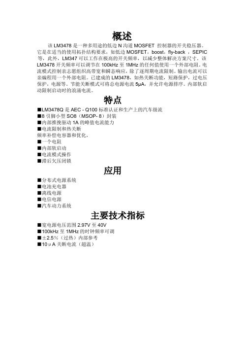
概述该LM3478是一种多用途的低边N沟道MOSFET 控制器的开关稳压器。
它是在适当的使用拓扑结构要求,如低边MOSFET,boost,fly-back ,SEPIC 等,此外,LM347可以工作在极高的开关频率,以减少整体解决方案尺寸。
该LM3478开关频率可以调节在100kHz至1MHz的任何值使用一个外部电阻。
电流模式控制亲志愿组织高带宽和瞬态响应,除了逐周期电流限制。
输出电流可以亲编程用一个外部电阻。
已建成的LM3478,如热关断功能,短路保护,过电压保护,电源等。
节能关断模式可将总电源电流5μA,并允许电源排序。
内部软启动限制启动时的浪涌电流。
特点■LM3478Q是AEC - Q100标准认证和生产上的汽车级流■8引脚小型SO8(MSOP- 8)封装■内部推挽驱动1A的峰值电流能力■电流限制和热关断频率补偿电容器和优化,■一个电阻■内部软启动■电流模式操作■滞后欠压闭锁应用■分布式电源系统■电池充电器■离线电源■电信电源■汽车动力系统主要技术指标■宽电源电压范围2.97V至40V■100kHz至1MHz的时钟频率可调■±2.5%(过热)内部参考■10μA关断电流(超温)引脚名称引脚数说明I SEN 1 电流检测输入引脚。
在外部产生的电压电阻输入这个引脚。
COMP 2 补偿引脚。
一个电阻,电容的组合连接到本引脚为控制环路补偿。
FB 3 反馈引脚。
输出电压应调整使用一个电阻分压器提供该脚1.26V。
AGND 4 模拟接地引脚PGND 5 电源地引脚DR 6 驱动引脚。
外部MOSFET的栅极应连接到这个引脚。
FA/SD 7 频率调整和关机引脚。
连接到该管脚的电阻设定振荡器的频率。
该管脚的高层次的时间超过30微秒将关闭设备。
该装置将绘制小于10μA从供给V IN8 电源输入引脚典型的高效率升压型(升压)转换器。

高效率峰值电流控制升压DC-DC转换器设计的开题报告
一、选题背景与意义
直流电源电压通常比较低,对于一些特殊场合需要高功率输出的设备,需要升压转换器来提高直流电压。
同时,要保证转换过程中能够尽可能地提高效率,减少能源的损耗。
因此,设计一种高效率峰值电流控制升压DC-DC转换器,能够提高升压的效率,并且使得升压的过程更加稳定和可靠,对于提高节能降耗具有重要意义。
二、研究内容和目标
本研究的目的是设计一种高效率峰值电流控制升压DC-DC转换器,主要研究内容如下:
1. 分析升压DC-DC转换器的原理并且设计出合理的电路结构。
2. 选取合适的元器件并进行参数的选型,包括电感、电容、MOSFET等元器件,保证电路的稳定性和效率。
3. 进行仿真和实验验证,对电路进行有效的测试和评估,为实际应用提供科学依据。
三、研究方法和技术路线
1. 确定升压DC-DC转换器的工作原理,结合控制电路展开电路设计。
2. 选定合适的电感、电容、MOSFET等元器件并进行参数的选型。
3. 利用Matlab和Simulink平台,对升压DC-DC转换器进行建模和仿真。
4. 根据仿真结果,对电路进行优化调整。
5. 利用PCB设计软件进行电路布局和特殊场合的设计要求。
6. 制作电路板并进行实验验证,测试电路性能和效率,对结果进行分析和总结。
四、预期成果
这项研究的预期成果是设计出一种高效率峰值电流控制升压DC-DC转换器,能够提高升压的效率,并且使得升压的过程更加稳定和可靠,从而为实际应用提供科学依据。
同时,该项目的研究成果也将在电子、通信等领域得到广泛的应用。
升降压电路原理分析电源网讯Buck变换器:也称降压式变换器,是一种输出电压小于输入电压的单管不隔离直流变换器。
图中,Q为开关管,其驱动电压一般为PWM(Pulse width modulation脉宽调制)信号,信号周期为Ts,则信号频率为f=1/Ts,导通时间为Ton,关断时间为T off,则周期Ts=Ton+Toff,占空比Dy= T on/Ts。
Boost变换器:也称升压式变换器,是一种输出电压高于输入电压的单管不隔离直流变换器。
开关管Q也为PWM控制方式,但最大占空比Dy必须限制,不允许在Dy=1的状态下工作。
电感Lf在输入侧,称为升压电感。
Boost变换器也有CCM和DCM两种工作方式Buck/Boost变换器:也称升降压式变换器,是一种输出电压既可低于也可高于输入电压的单管不隔离直流变换器,但其输出电压的极性与输入电压相反。
Buck/Boost变换器可看做是Buck变换器和Boost变换器串联而成,合并了开关管。
Buck/Boost变换器也有CCM和DCM两种工作方式,开关管Q 也为PWM控制方式。
LDO的特点:① 非常低的输入输出电压差② 非常小的内部损耗③ 很小的温度漂移④ 很高的输出电压稳定度⑤ 很好的负载和线性调整率⑥ 很宽的工作温度范围⑦ 较宽的输入电压范围⑧ 外围电路非常简单,使用起来极为方便DC/DC变换是将固定的直流电压变换成可变的直流电压,也称为直流斩波。
斩波器的工作方式有两种,一是脉宽调制方式Ts不变,改变ton(通用),二是频率调制方式,ton不变,改变Ts(易产生干扰)。
其具体的电路由以下几类:(1)Buck电路——降压斩波器,其输出平均电压U0小于输入电压Ui,极性相同。
(2)Boost电路——升压斩波器,其输出平均电压U0大于输入电压Ui,极性相同。
(3)Buck-Boost电路——降压或升压斩波器,其输出平均电压U0大于或小于输入电压Ui,极性相反,电感传输。
正确运用DC-DC降压/升压调节器进行设计
DC-DC 开关转换器的作用是将一个直流电压有效转换成另一个。
高效率DC-DC转换器采用三项基本技术:降压、升压,以及降压/升压。
降压转换器用于产生低直流输出电压,升压转换器用于产生高直流输出电压,降压/升压转换器则用于产生小于、大于或等于输入电压的输出电压。
本文将重点介绍如何成功应用降压/升压DC-DC转换器。
降压和升压转换器已在2011年6月和9月的《模拟对话》中单独介绍过,此处将不再赘述。
降压/升压调节器内置四个开关、两个电容和一个电感,如
当VIN大于VOUT,时,开关C断开,开关D闭合。
开关A和B的工作方式和在标准降压调节器中一样,如
当VIN小于VOUT,时,开关B断开,开关A闭合。
开关C和D的工作方式和在升压调节器中一样,如
对于高负载电流,降压/升压调节器采用电流模式、固定频率、脉冲宽度调制(PWM)控制,以获得出色的稳定性和瞬态响应。
为确保便携式应用的电池寿命最长,还采用了省电模式,在轻载时可降低开关频率。
对于无线应用和其它低噪声应用,可变频率省电模式可能会引起干扰,通过增加逻辑控制输入,可强制转换器在所有负载条件下均以固定频率PWM方式工作。
降压/升压调节器提高系统效率
如今的很多便携式系统都采用单单元锂离子充电电池供电。
如上所述,电池会从满充状态时的4.2 V开始工作,缓慢放电至3.0 V。
当电池输出降至3.0 V以下时,系统就会关闭,防止电池因过度放电而受损。
采用低压差调节器产生3.3 V电压轨时,系统会在。
Application ReportSNVA035B–November1999–Revised April2013 AN-1066Low Cost Boost Converters Using LM3578AABSTRACTThe LM3578A integrated circuit is a switching regulator with all the power,control,and protection features.It operates over a wide input voltage range.This together with its low-cost makes it a very popular choice for use in switching regulators.This application report presents several low-cost boost converter circuits developed using the LM3578A switching regulator.The operation and the design of the boost converter is also discussed in detail.Contents1Introduction (2)1.1Modes of Operation (2)1.2Continuous Versus Discontinuous Mode (3)2Selection of Boost Power Stage Components (3)2.1Selection of the Boost Inductor (3)2.2Selection of Power Switch (4)2.3Selection of the Output Capacitor (4)2.4Selection of the Input Capacitor (5)2.5Selection of the Output Diode (5)3Low-Cost Boost Converters (5)3.1Voltage Doubler Circuit (5)3.2Boost Converter for Wide Band Tuners (6)3.3Low-Cost Boost Circuit for I/O Cards (7)4Summary (9)5References (9)Appendix A PCB Layout (10)List of Figures1Basic Boost Topology (2))Waveforms (2)2Inductor Current(iL3Low-Cost Voltage Doubler Circuit (6)45V to27V Boost Converter (7)5Low-Cost Boost Converter (8)6PCB Layout for the Circuits Shown in and(Scale:2:1) (10)7PCB Layout for the Circuit Shown in(Scale:2:1) (11)List of Tables1Parts List (6)2Parts List (7)3Parts List (9)All trademarks are the property of their respective owners.Introduction 1IntroductionThe boost or step-up converter converts a DC voltage to a higher DC voltage.Figure1shows the basic boost topology.When the switch software is turned on,energy is stored in the inductor L and the inductorcurrent iL ramps up at a slope determined by the input voltage.Diode D is off during this period.Once theswitch,SW,turns off,diode D starts to conduct and the energy stored in the inductor is released to the load.Current in the inductor ramps down at a slope determined by the difference between the input and output voltages.1.1Modes of OperationBased on the amount of energy that is delivered to the load during each switching period,the boostconverter can be classified into continuous or discontinuous conduction mode.If all the energy stored in the inductor is delivered to the load during each switching cycle,the mode of operation is classified as discontinuous conduction mode(DCM).In this mode,the inductor current ramps down all the way to zero during the switch off-time.If only part of the energy is delivered to the load,then the converter is said to be operating in continuous conduction mode(CCM).Figure2shows the inductor current waveforms for all the modes of operation.The mode of operation is a fundamental factor in determining the electrical characteristics of theconverter.The characteristics vary significantly from one mode to the other.Figure1.Basic Boost TopologyFigure2.Inductor Current(iL)Waveforms Selection of Boost Power Stage Components1.2Continuous Versus Discontinuous ModeBoth modes of operation have advantages and disadvantages.The main disadvantage in using CCM is the inherent stability problems (caused by the right-half-plane zero and the double pole in the small-signal control to output voltage transfer function).However,the switch and output diode peak currents are larger when the converter is operating in discontinuous rger peak currents necessitate using power switch and output diode with larger current and power dissipation rger peak currents also force the designer to use larger output capacitors.The larger peak currents also cause greater EMI/RFI problems.The mode of operation can be selected by the user.For very low load currents,discontinuous mode is preferred over continuous mode.If the load current requirements are high,then in order to minimize the peak currents and the associated problems,continuous mode is preferred.Two of the circuits presented in Section 3have very low load current requirements.Hence,they have been selected to operate indiscontinuous mode.The third circuit has very high peak current requirements and is selected to operate in continuous mode.2Selection of Boost Power Stage ComponentsThe boost converter design involves the selection of the inductor,the input and output capacitors,the power switch (included in the LM3578A),and the output diode.In order to select these components,it is necessary to know the duty cycle range and the peak currents.Knowing the maximum and minimum input voltages,the output voltage,and the voltage drops across the output diode and the switch,the maximum and minimum duty cycles are calculated.Next,the average inductor current can be estimated from the load current and duty cycle.Now,assuming the peak-to-peak inductor current ripple to be certain percentage of the average inductor current ripple,the peak inductor current can be estimated.The inductor value can be calculated using the ripple current,switching frequency,input voltage,and duty cycle information.Finally,it is necessary to establish the boundary condition,that is,the critical value of the inductor that the converter will operate in discontinuous mode.Once the inductor value has been chosen and the peak currents have been established,the other components can be selected very easily.The following paragraphs outline the selection of the boost power stage components,in a step-by-step approach.2.1Selection of the Boost InductorStep 1:Given the maximum and minimum input voltages,the maximum and minimum duty cycles can calculated using Equation 1and Equation 2:(1)(2)In Equation 1and Equation 2,V O is the output voltage,V d is the forward voltage drop of the output diode D,and V ce(sat)is the on state voltage of the switch,SW.V in(max)and V in(min)are the maximum and minimum input voltages,respectively.Step 2:The average inductor current (maximum)can be calculated using the output current,I O as shown in Equation 3:(3)Step 3:Assume the peak-to-peak inductor current ripple,Δi L to be a certain percentage of the average inductor current calculated in Equation 3.The peak inductor current is then given by:(4)Selection of Boost Power Stage Components Step 4:Knowing the switching frequency,f s the required inductance value can be selected using Equation 5:(5)Step 5:Calculate the boundary condition,that is,the minimum inductance required to operate the inductor in continuous mode.At the boundary between CCM and DCM modes of operation,the peak inductor current,I p is same as the peak-to-peak inductor current ripple,Δi L ,as shown in Figure 2.Hence,the average inductor current is given by:(6)Using Equation 3and Equation 6(7)The critical value of the inductance to maintain the converter in continuous mode of operation,derived from Equation 5and Equation 7is given by:(8)Using an inductance value lower than the critical value will result in discontinuous mode of operation.It can also be observed from Equation 5Equation 8that increasing the switching frequency helps in reducing the size of the inductor.2.2Selection of Power SwitchThe power switch is internal to the LM3578A.In general ,it is necessary to ensure that the estimated peak switch current (which is nothing but the peak inductor current,I p calculated in Equation 8)does not exceed the rated current of the switch.It is also necessary to ensure that the off-state voltage rating of the switch is never exceeded.The internal transistor in the LM3578A switching regulator is rated for a peak current of 750mA.The off-state sustaining voltage of the internal transistor is 50V.2.3Selection of the Output CapacitorIn the boost converter,the instantaneous value of currents entering and exiting the output capacitor is very high,since there is no inductive element between the output diode and the capacitor.This high current flows through the equivalent series resistance (ESR)and equivalent series inductance (ESL)of thecapacitor.ESR increases the capacitor temperature and increases ripple voltage.ESL adds sharp spikes to the ripple voltage waveform.Hence,it is desired to use output capacitors with very low ESR and ESL.The peak-to-peak output ripple voltage,ΔV O ,is given by:(9)where I Omax is the maximum output current.The output capacitor,C O can be selected using Equation 9.It should be noted that the ripple voltage due to the ESR,(R esr )is dominant in Equation 9.Also,ESL adds sharp spikes over the ripple voltage given by Equation 9.The ESR of the selected capacitor can be determined from the manufacturer catalogs or by actual bench measurement.If the value of the ripple exceeds the desired ripple voltage,then there are two choices:paralleling two or more capacitors to lower the effective ESR and ESL,or using a secondary LC filter.In general,low values of ESR are achieved by using large value capacitors or by paralleling smaller value capacitors.NOTE:Tantalum capacitors are known to have very low ESR.But they are expensive whencompared to electrolytic capacitors. Low-Cost Boost Converters2.4Selection of the Input CapacitorIn boost switching regulators,triangular ripple current is drawn from the supply voltage due to theswitching action.This appears as noise on the input line.This problem is less severe in boost converter due to the presence of inductor in series with input line.Select the input capacitor for:(10)From Equation 10,it can be observed that the rms current value is very low.Hence,a very small value capacitor is sufficient for boost converters.2.5Selection of the Output DiodeAs in all switching power supplies,two factors govern the choice of output rectifier:the forward voltage drop,V F ,and the reverse recovery time,t rr .V F determines the forward conduction loss and should be as low as possible.The reverse recovery time of the diode (and also the forward recovery time)should be as low as possible for minimizing the switching losses and RFI problems.Schottky rectifiers have very low forward voltage drops and reverse recovery times.The maximum reverse bias voltage on the output rectifier is given by:V r =V o −V ce(sat)(11)Select a Schottky diode satisfying the reverse voltage and peak current ratings given by Equation 4Equation 11,respectively.3Low-Cost Boost ConvertersThis section presents several low-cost boost circuits based on the LM3578A switching regulator.The LM3578A IC is a switching regulator featuring an internal comparator,oscillator,protection circuitry and a transistor.This IC operates from supply voltages ranging from 2V to 40V.This wide supply voltage range,together with its low cost makes it very popular.The transistor internal to LM3578A can handle currents only up to 750mA.However,for higher load current requirements,this internal transistor can be used to drive an external transistor with higher current rating such as the npn transistor,D44C3A.3.1Voltage Doubler CircuitFigure 3shows a low-cost voltage doubler circuit used typically in the RF card of a cable modem .This converter uses the LM3578A switching regulator for performing the required power conversion.Theinductor and other power stage components are selected using the procedure discussed in Section 2.The converter specifications are as follows:Input Voltage,V IN =12V Output Voltage V OUT =24V Load Current I L =10mA (max.)Switching Frequency,f s =100kHzSince the load current requirements are very low,this converter is chosen to operate in discontinuous conduction mode.The output voltage is maintained at 24V by the feedback network consisting of theresistors,R f1and R f2.The reference pin (pin 1)is set at 1V using these resistors.Capacitor C IN2is needed to ensure low noise at the input.The switching frequency is set by using the timing capacitor C T .Choosing a value of 680pF for C T sets the switching frequency at 100kHz.Capacitor C 1(typically between 10-25pF),together with the feedback resistors (R F1and R F2),is used for compensation.For more details on the choice of the above components,see the LM2578A/LM3578A Switching Regulator Data Sheet (SNVS767).Low-Cost Boost Converters Figure 3.Low-Cost Voltage Doubler CircuitTable 1.Parts ListDesignatorValue/RatingDescriptionIC1—LM3578M,Switching Regulator D 40V,0.5A MBR0540T1,Output DiodeL 470µH,60mA Boost Inductor C IN147µF,16V Input Capacitor C IN20.1µF,50V Input Capacitor (Ceramic)C OUT 22µF,35VOutput Capacitor R F1100k Feedback Resistor R F25k Feedback Resistor C F 22pF Feedback CapacitorC T680pFTiming Capacitor,Sets the Switching Frequency3.2Boost Converter for Wide Band TunersFigure 4shows a 5V to 27V boost converter used typically to create a high voltage for wide band tuners.Wide band cable and DSS tuners require about 27V at 5mA load current to bias the VCO varactor.The converter specifications are as follows:Input Voltage,V IN =5V Output Voltage,V OUT =27V Load Current I L =20mA (max.)Switching Frequency,f s =90kHz Input Ripple Voltage:17mV Output Ripple Voltage:58mVThe design of this circuit is very straightforward and is very similar to the design of the voltage doubler circuit discussed above.As in previous case,since the load current requirements are very low,thisconverter is chosen to operate in discontinuous conduction mode.The feedback resistors (R F1and R F2),the timing capacitor,C T and the compensation capacitor,C C are chosen in the same way.In order toensure low noise at the input,it is essential to add a high-frequency ceramic capacitor C IN2at the input rail,as shown in Figure 4. Low-Cost Boost ConvertersFigure4.5V to27V Boost ConverterTable2.Parts ListDesignator Value/Rating DescriptionIC1—LM3578M,Switching RegulatorD40V,0.5A MBR0540T1,Output DiodeL100µH,100mA Boost InductorC IN147µF,10V Input CapacitorC IN20.1µF,10V Input Capacitor(Ceramic)C OUT22µF,35V Output CapacitorR F1130k Feedback ResistorR F25k Feedback ResistorC F22pF Feedback CapacitorC T820pF Timing Capacitor,Sets the Switching Frequency3.3Low-Cost Boost Circuit for I/O CardsFigure5shows a low-cost boost converter that converts a3.3V input to5V at600mA load current.This circuit is typically used in I/O cards.Converter Specifications:Input Voltage,V=3.3V(±10%)inOutput Voltage=5V(±5%)Output Current=0mA–600mAEfficiency=80%The maximum and minimum duty cycles calculated using Equation1and Equation2are equal to0.52 and0.4,respectively.The average inductor current calculated using Equation3is:(12)Low-Cost Boost Converters Assuming the peak-to-peak ripple current to be 50%of the average inductor current,the peak current calculated using Equation 4is equal to:(13)The peak current calculated above is very much higher than the rated current of the internal switch in the LM3578A.Hence,it is necessary to use an external transistor or a FET.The selected external switchshould be capable of handling the high peak currents.The internal transistor in LM3578A can handle up to 750mA.So the current gain of the external transistor should be sufficient at the peak primary current.The off state voltage rating,V CE ,of the transistor should be at least 10V.One npn transistor meeting these requirements is D44C3A.The current gain (h fe )of this transistor at the peak current of 1.563A is about 50.So the maximum current that the internal transistor needs to provide is equal to 1.563/50=31mA,which is very much less than the rated current of the internal transistor.The circuit shown in Figure 5performs the required conversion using LM3578A and D44C3A npntransistor.The power stage components are selected using the procedure discussed in Section 2.From the above calculations,it can be seen that the peak current requirements are very high.Hence,this converter is chosen to operate in continuous conduction mode.The boost converter operating incontinuous mode has inherent stability problems (due to the right half plane zero and the double pole in the small-signal control to output transfer function).Hence,additional compensation is needed in thecontrol loop.This additional compensation is provided by the capacitor C C1(typically around 1nF)and the resistor R C1(typically between 100k and 200k).The current limiting in this circuit is activated whenever pin 7is pulled 110mV above the ground.The voltage across the current sense resistor,R sn is sensed in order to prevent excessive current through the external switch.The value of R sn is given by:(14)where I lim is the desired current limit set point.As an example,for the circuit shown in Figure 5,the peak switch current calculated above is 1.563A.Hence,if the desired current,I lim is set at 2A,then the value of the current-sense resistor will be R sn =0.110/2=0.055Ω.For cost reasons,the current-sense resistor can also be fabricated on a copper trace.Reference [1]describes the procedure for calculating the trace length and width.Figure 5.Low-Cost Boost Converter SummaryTable3.Parts ListDesignator Value/Rating DescriptionIC1—LM3578A Switching RegulatorQ15A,30V D44C3A,NPM TransistorD11A,40V Diode,1N5819L Lp-33µH,Ip-2.0A InductorC in220µF,6.3V Input CapacitorC o2x220µF,10V Output CapacitorR sn0.050Ω,1W Current Sense Resistor/Copper TraceR F140.06k,1/4W Feedback ResistorR F210k,1/4W Feedback ResistorR d11Ω,1/4W Base Drive ResistorR d2200Ω,1/4W Base Drive ResistorR f2000Ω,1/4W Resistor for Spike SuppressionC f1nF Capacitor for Spike SuppressionC T820pF Timing CapacitorC c22pF Compensation CapacitorC c11nF Compensation CapacitorR c1140k Compensation Capacitor4SummarySeveral low-cost boost converters,designed using the LM3578A switching regulator,were presented in this document.The circuits can be used in many different applications.The parts list has been provided for these circuits.Recommended layouts for these circuits were presented in Appendix A.The layout is very critical in these circuits.Pins1,2,and7of LM3578A are very noise sensitive.So these pins should be placed away from high frequency noise sources in the circuit.It is also necessary to have the feedback trace away from the inductor.In order to avoid false triggering of current limiting circuitry, filtering is very much essential for the sensed current.It is also important to note that the current sense voltage shut down level has very high tolerance.The voltage can vary from80mV to160mV(typicalvalue is100mV).This factor should be taken into consideration while selecting the current sense resistor.The compensation capacitor,CC connected between pins1and3should be typically between10to25ing a larger value for CC will start effecting the switching frequency.It is also necessary to note thatLM3578A can skip pulses at very low load currents when the minimum duty cycle of each pulse provides more energy than the load demands.Under these conditions,the controller internal to the LM3578A starts skipping pulses to maintain the output voltage at its correct value.This mode of operation is also known as burst mode.Although only three boost circuits have been presented,the design approach for other voltage and current levels is the same.5References1.AN-1055Low-Cost Multiple Output Flyback Converter for I/O Cards(SNOA383)2.LM2578A/LM3578A Switching Regulator Data Sheet(SNVS767)3.National Power ICs Databook Appendix A PCB LayoutFigure6.PCB Layout for the Circuits Shown in Figure3and Figure4(Scale:2:1) Appendix ANote:Copper trace is used as current sense resistor.Figure7.PCB Layout for the Circuit Shown in Figure5(Scale:2:1)11 SNVA035B–November1999–Revised April2013AN-1066Low Cost Boost Converters Using LM3578A Submit Documentation FeedbackCopyright©1999–2013,Texas Instruments IncorporatedIMPORTANT NOTICETexas Instruments Incorporated and its subsidiaries(TI)reserve the right to make corrections,enhancements,improvements and other changes to its semiconductor products and services per JESD46,latest issue,and to discontinue any product or service per JESD48,latest issue.Buyers should obtain the latest relevant information before placing orders and should verify that such information is current and complete.All semiconductor products(also referred to herein as“components”)are sold subject to TI’s terms and conditions of sale supplied at the time of order acknowledgment.TI warrants performance of its components to the specifications applicable at the time of sale,in accordance with the warranty in TI’s terms and conditions of sale of semiconductor products.Testing and other quality control techniques are used to the extent TI deems necessary to support this warranty.Except where mandated by applicable law,testing of all parameters of each component is not necessarily performed.TI assumes no liability for applications assistance or the design of Buyers’products.Buyers are responsible for their products and applications using TI components.To minimize the risks associated with Buyers’products and applications,Buyers should provide adequate design and operating safeguards.TI does not warrant or represent that any license,either express or implied,is granted under any patent right,copyright,mask work right,or other intellectual property right relating to any combination,machine,or process in which TI components or services are rmation published by TI regarding third-party products or services does not constitute a license to use such products or services or a warranty or endorsement e of such information may require a license from a third party under the patents or other intellectual property of the third party,or a license from TI under the patents or other intellectual property of TI.Reproduction of significant portions of TI information in TI data books or data sheets is permissible only if reproduction is without alteration and is accompanied by all associated warranties,conditions,limitations,and notices.TI is not responsible or liable for such altered rmation of third parties may be subject to additional restrictions.Resale of TI components or services with statements different from or beyond the parameters stated by TI for that component or service voids all express and any implied warranties for the associated TI component or service and is an unfair and deceptive business practice. TI is not responsible or liable for any such statements.Buyer acknowledges and agrees that it is solely responsible for compliance with all legal,regulatory and safety-related requirements concerning its products,and any use of TI components in its applications,notwithstanding any applications-related information or support that may be provided by TI.Buyer represents and agrees that it has all the necessary expertise to create and implement safeguards which anticipate dangerous consequences of failures,monitor failures and their consequences,lessen the likelihood of failures that might cause harm and take appropriate remedial actions.Buyer will fully indemnify TI and its representatives against any damages arising out of the use of any TI components in safety-critical applications.In some cases,TI components may be promoted specifically to facilitate safety-related applications.With such components,TI’s goal is to help enable customers to design and create their own end-product solutions that meet applicable functional safety standards and requirements.Nonetheless,such components are subject to these terms.No TI components are authorized for use in FDA Class III(or similar life-critical medical equipment)unless authorized officers of the parties have executed a special agreement specifically governing such use.Only those TI components which TI has specifically designated as military grade or“enhanced plastic”are designed and intended for use in military/aerospace applications or environments.Buyer acknowledges and agrees that any military or aerospace use of TI components which have not been so designated is solely at the Buyer's risk,and that Buyer is solely responsible for compliance with all legal and regulatory requirements in connection with such use.TI has specifically designated certain components as meeting ISO/TS16949requirements,mainly for automotive use.In any case of use of non-designated products,TI will not be responsible for any failure to meet ISO/TS16949.Products ApplicationsAudio /audio Automotive and Transportation /automotiveAmplifiers Communications and Telecom /communicationsData Converters Computers and Peripherals /computersDLP®Products Consumer Electronics /consumer-appsDSP Energy and Lighting /energyClocks and Timers /clocks Industrial /industrialInterface Medical /medicalLogic Security /securityPower Mgmt Space,Avionics and Defense /space-avionics-defense Microcontrollers Video and Imaging /videoRFID OMAP Applications Processors /omap TI E2E Community Wireless Connectivity /wirelessconnectivityMailing Address:Texas Instruments,Post Office Box655303,Dallas,Texas75265Copyright©2013,Texas Instruments Incorporated。
2004级电力电子技术课程设计报告姓名:学号:班级:指导老师:专业:电气工程与自动化设计时间:降压斩波变换技术的应用---D C /D C 变换器的设计与实现摘要:介绍了一种新颖的具有升降压功能的DC /DC 变换器的设计与实现,具体地分析了该DC /DC 变换器的设计(拓扑结构、工作模式和储能电感参数设计),详细地阐述了该DC /DC 变换器控制系统的原理和实现,最后给出了测试结果关键词:DC /DC 变换器,降压斩波,升压斩波,储能电感,直流开关电源,PWM ;直流脉宽调速降压斩波原理图:RE U I E E T t t t E t U Mon off on on -===+=000α式中on t 为V 处于通态的时间;off t 为V 处于断态的时间;T 为开关周期;α为导通占空比,简称占空比火导通比。
根据对输出电压平均值进行调制的方式不同,斩波电路有三种控制方式:1) 保持开关周期T 不变,调节开关导通时间on t 不变,称为PWM 。
2) 保持开关导通时间on t 不变,改变开关周期T ,称为频率调制或调频型。
3) on t 和T 都可调,使占空比改变,称为混合型。
i E M● 工作原理➢t =0时刻驱动V 导通,电源E 向负载供电,负载电压u o=E ,负载电流i o 按指数曲线上升➢t =t 1时刻控制V 关断,负载电流经二极管VD 续流,负载电压u o 近似为零,负载电流呈指数曲线下降。
为了使负载电流连续且脉动小通常使串接的电感L 值较大● 基于“分段线性”的思想,对降压斩波电路进行解析● 从能量传递关系出发进行的推导●由于L 为无穷大,故负载电流维持为I o 不变●电源只在V 处于通态时提供能量,为E 0I on t●在整个周期T 中,负载消耗的能量为(R 0I T+M E 0I T )一周期中,忽略损耗,则电源提供的能量与负载消耗的能量相等RE U I E E T t t t E t U M on off on on -===+=000α输出功率等于输入功率,可将降压斩波器看作直流降压变压器该电路使用一个全控器件V ,途中为IGBT ,也可使用其他器件,若采用晶闸管,需设置晶闸管关断的辅助电路。
鍒╃敤LM3478璁捐50W DC-DC鍗囬檷鍘嬪彉鎹㈠櫒
銆€銆€寮曡█
銆€銆€鐜颁唬鐢靛瓙鎶€鏈彂灞曞緢蹇紝鍗婂浣撲緵搴斿晢涓嶆柇鎺ㄥ嚭鏂板櫒浠讹紝浠庤€屾帹鍔ㄧ數瀛愬簲鐢ㄥ伐绋嬪笀鐨勪笉鏂垱鏂拌璁★紝浠ユ弧瓒冲競鍦虹殑鏃ョ泭闇€姹傘€傛湰鏂囦粙缁嶇殑鍗虫槸鍩轰簬瀹㈡埛鐨勯渶姹傦紝搴旂敤缇庡浗鍥藉鍗婂浣撳叕鍙哥殑鏂板瀷鐢垫祦鍨婸WM鑺墖LM3478鍙婂熀浜嶴EPIC鍗囬檷鍘嬪師鐞嗗疄鐜扮殑50WDC-DC閫傞厤鍣ㄣ€傝閫傞厤鍣ㄧ殑涓昏鐗圭偣鏄細鐩存祦杈撳叆鐢靛帇鑼冨洿鏋佸锛涜緭鍑哄姛鐜囧ぇ锛涗繚鎶ゅ姛鑳藉叏锛涜緭鍑虹汗娉㈠皬锛涙晥鐜囬珮锛涘伐浣滅ǔ瀹氬彲闈狅紱搴旂敤鑼冨洿骞裤€?
銆€銆€SEPIC鍨嬪彉鎹㈠櫒
銆€銆€SEPIC鐨勭數姘斿師鐞嗙畝鍥俱€?
銆€銆€閫氬父绉颁箣涓哄崌闄嶅帇鍙樻崲鍣⊿EPIC鐨勭畝鍗曞師鐞嗗涓嬶細褰揝W寮€閫氭椂锛屽姞鍦↙1锛孡2涓婄殑鐢靛帇鍧囦负Vin锛屾鏃禖p骞跺湪L2涓婏紝涓旀湁Cp 涓婄殑鐢靛帇涓嶭2涓婄殑鐩哥瓑銆傚綋SW鍏虫柇鏃讹紝L1涓殑鐢垫祦缁х画娌跨潃Cp 銆丏1娴佸悜Cout杈撳嚭鍒拌礋杞斤紝鍚屾椂L2鐨勭數娴佷篃娴佸悜D1銆丆out杈撳嚭鍒拌礋杞姐€傚湪姝ゆ湡闂达紝閫氳繃L1銆丩2鐨勭數鍘嬪潎绛変簬杈撳嚭鐢靛帇Vout銆傜敱SEPIC鐨勫師鐞嗗彲鎺ㄥ嚭鍩烘湰鍏崇郴寮忥細Vout/Vin锛滵/(1-D)銆傚紡涓璂涓哄崰绌烘瘮锛屼笖蹇界暐SW鍙奓1绛夌殑鍘嬮檷銆?
銆€銆€LM3478
銆€銆€LM3478鑺墖鐨勪富瑕佺壒鐐癸細
銆€銆€·瀹借緭鍏ョ數鍘?2.79—40VDC
銆€銆€·楂樺伐浣滈鐜?100KHz—1MHz
銆€銆€·寰瀷灏佽:MSOP-8
銆€銆€·椹卞姩鐢垫祦:1A
銆€銆€·鍐呴儴闄愬埗:OCP,OVP,LVP,OTP
銆€銆€·宸ヤ綔娓╁害:-40鈩?mdash;+125鈩?
銆€銆€50WDC-DC鍙樻崲鍣ㄨ璁?
銆€銆€璇ュ彉鎹㈠櫒鐨勪富瑕佹妧鏈姹傦細
銆€銆€鐩存祦杈撳叆鐢靛帇鑼冨洿锛?-60VDC
銆€銆€杈撳叆鐢垫祦锛氾紲6A(9VDC)
銆€銆€鐩存祦杈撳嚭鐢靛帇锛?2VDC±%
銆€銆€鐩存祦杈撳嚭鐢垫祦锛?.5A
銆€銆€杈撳嚭绾规尝鐢靛帇锛氾紲100mVRMS
銆€銆€棰濆畾鍔熺巼锛?2W
銆€銆€宄板€煎姛鐜囷細50W
銆€銆€鐢垫簮鏁堢巼锛氬吀鍨嬪€?5%锛涙弧璐熻浇
銆€銆€淇濇姢鍨嬪紡锛氱數娴侀檺鍒跺姛鐜囦繚鎶?
銆€銆€杈撳嚭杩囨祦淇濇姢锛氾紲4.2A
銆€銆€杈撳嚭杩囧帇淇濇姢锛氱敱LM3478鎺у埗
銆€銆€宸ヤ綔娓╁害鑼冨洿:-20鈩?mdash;锛?0鈩?
銆€銆€瀹夎鍙奅MC绗﹀悎鍥介檯鏍囧噯
銆€銆€楂樺彲闈犳€TBF锛?00,000灏忔椂
銆€銆€澶栧瀷鍙婂昂瀵革細濉戝3寮忥紱102×46×25(mm)
銆€銆€50WDC-DC鍙樻崲鍣ㄧ殑鐢垫皵鍘熺悊鍥俱€?
銆€銆€璇ョ數璺槸鍩轰簬SEPIC鎷撴墤銆佸簲鐢↙M3478鑺墖鎸夌収瀹㈡埛鐨勬妧鏈姹傝璁$殑銆傚湪璇ョ數璺腑锛岃€冭檻鍒伴€傞厤鍣ㄧ殑浣撶Н鍙婂偍鑳界數鎰熺鎬ф潗鏂欑殑浣撶Н锛岄€夊畾宸ヤ綔棰戠巼Fs锛?50KHz銆?
銆€銆€璁$畻鍌ㄨ兘鐢垫劅L3銆丩4鐨勭數鎰熼噺鍙婄鑺€夋嫨
銆€銆€棣栧厛鐢卞叕寮忥細D锛漋out/(Vout+Vin)璁$畻鍗犵┖姣斻€傜敱浜庢渶涓ラ叿鏉′欢涓嬬殑鐢垫劅绾规尝鐢垫祦鏄湪鏈€澶ц緭鍏ョ數鍘嬩笅锛屾墍浠锛?2/(12+60)≈0.167銆?
銆€銆€璁$畻鍌ㄨ兘鐢垫劅l3銆丩4锛氭甯告儏鍐典笅锛孡4鐨勫ぇ灏忓湪纭繚鏈€灏忚礋杞界數娴佷笅浣跨數鎰熺數娴佽繛缁紝涓旇緭鍑虹汗娉㈡弧瓒虫寚鏍囪姹傘€備负姝わ紝鎴戜滑鍋囧畾鍦?0%鏈€灏忚礋杞界數娴佷笅锛屽厑璁告湁40%鐨勫嘲-宄板€肩汗娉㈢數娴佹祦杩嘗4銆?
銆€銆€C1銆丆2涓鸿緭鍏ユ护娉紝Q1銆丏Z1銆丏Z2銆丏1-1鏋勬垚鍚姩鐢垫簮锛孡3銆丩4涓哄偍鑳界數鎰燂紝Q2涓哄姛鐜嘙OSFET锛孖C涓篜WM椹卞姩鑺墖锛孯5涓洪鐜囪皟鏁寸數闃伙紝C3銆丆4銆丷2涓哄弽棣堣ˉ鍋匡紝R3銆丷4涓哄弽棣堝垎鍘嬬數闃伙紝R7涓鸿繃鐢垫祦鍙栨牱鐢甸樆锛孋8銆丆9涓篠EPIC鐢靛锛孯8銆丷9銆丆6銆丆7涓哄惛鏀剁綉缁滐紝D2涓鸿緭鍑烘暣娴佷簩鏋佺锛孋10銆丆11銆丆12涓鸿緭鍑烘护娉㈢數瀹广€傚綋鐒惰鎯崇鍚圗MC瑕佹眰锛岃緭鍏ョ杩樺簲璇ユ湁鍏辨ā鐢垫劅锛屽樊妯$數鎰燂紝鍙奨銆乊绛夊畨瑙勭數瀹广€?
銆€銆€L锛漋×dt/di锛?
銆€銆€鍏朵腑dt锛?/Fs×D锛?/(250×103)×0.167≈0.668锛孷涓篤in鍦∕OSFET寮€閫氭椂鐨勫€笺€傚洜姝わ紝鏈夊涓嬭绠楋細
銆€銆€L4锛?0×(0.668×10-6/0.4)锛?00.2μH銆傚彇100μH鐨勬爣绉板€笺€傜敱璇EPIC鍘熺悊鍙婅璁$粡楠屽彲鐭ワ紝浣滀负淇╀釜鍒嗙鐨勫偍鑳界數鎰燂紝L3鐨勫彇鍊间篃涓猴細100μH銆?
銆€銆€鐢变簬璇ョ數鎰熶负鍌ㄨ兘鐢垫劅锛屽洜姝わ紝瀵圭鎬ф潗鏂欑殑閫夊彇瑕佺壒鍒敞鎰忋€傛澶勯€夋嫨鐨勬潗鏂欎负锛歁agnetic鍏徃鐨凨oolMu锛岀浉鍚屾€ц兘鐨勬潗鏂欙紝鍏朵粬鍏徃鍙堢О閾佺閾濄€傚弬鏁板涓嬶細
銆€銆€·鏂欏彿锛?7381-A7锛岄粦鑹?
銆€銆€·灏哄锛?7.27×9.65×6.35(mm)锛屼负鐜瀷纾佽姱
銆€銆€·鐢垫劅鍥犳暟AL锛?3(nH/N2)锛孨涓哄湀鏁?
銆€銆€鐢卞叕寮忥細L锛滱L×N2锛屽彲浠ヨ绠楀嚭鐢垫劅鍦堟暟涓猴細
銆€銆€48鍦堬紝涓旂敤AWG18鍙风嚎缁曞埗銆侺3銆丩4鐩稿悓鍙傛暟銆?
銆€銆€·Magnetic鍏徃鐨凨oolMu鏉愭枡锛屾崯鑰楀皯锛岀浉瀵规垚鏈綆锛屼篃鍙互閫夊悓瑙勬牸鍏朵粬鍘傚晢閾佺閾濇潗鏂欍€傚鏋滄兂杩涗竴姝ラ檷浣庢垚鏈篃鍙互閫夌敤鍥戒骇鐨勯搧纭呴摑鏉愭枡銆?
銆€銆€涓婅堪L3銆丩4涓轰袱涓垎绂荤數鎰熻璁★紝涔熷彲浠ュ叡鐢ㄤ竴涓偍鑳界鐜紝鍙槸姝ゆ椂鐢变簬鑰﹀悎鐢垫劅鐨勫瓨鍦紝璁$畻鐨勭數鎰熷€间负涓婅堪鍊肩殑涓€鍗婏紝涓?0μH銆備絾鎴愭湰浣庝簺銆?
銆€銆€PCB娉ㄦ剰浜嬮」
銆€銆€鐢变簬涓洪珮棰慏C-DC鍙樻崲,鍥犳锛孭CB甯冪嚎寰堥噸瑕併€傚尯鍒嗗姛鐜囧湴涓庝俊鍙峰湴鐨勬眹娴佺偣锛岄┍鍔↖C涓嶮OSFET鐨勫叧绯伙紝杈撳叆婊ゆ尝涓庤緭鍑
烘护娉㈢殑浣嶇疆绛夈€傚悓鏃舵敞鎰忓垎绂诲厓浠跺強璐寸墖鍏冧欢鐨勪綅缃叧绯汇€傝繕瑕佽€冭檻鏁g儹鍣ㄧ殑褰㈢姸鍙婃暎鐑潰绉€?
銆€銆€鍏抽敭鍏冨櫒浠剁殑閫夋嫨鍙婅鏄?
銆€銆€鍔熺巼MOSFET鐨勯€夋嫨锛歂-FET锛屾瀬浣庡閫氱數闃伙紝浣庨棬鏋侀┍鍔ㄧ數鍘嬶細5V—7V锛岀鍚圥WM-IC瑕佹眰锛孴O-220AB灏佽锛?00V/85A锛岀粨娓?75鈩冦€傚瀷鍙蜂负VISHAY锛歋UP85N10-10銆?
銆€銆€鑲栫壒鍩烘暣娴佷簩鏋佺鐨勯€夋嫨锛氬瀷鍙蜂负MBR20100CT锛屽皝瑁呬负TO-220AB锛?00V/20A锛屾鍚戝帇闄嶄綆銆?
銆€銆€杈撳叆銆佽緭鍑烘护娉㈢數瑙g數瀹瑰彲鐢辫绠楀叕寮忔垨缁忛獙閫夊彇銆侰8銆丆9鍙敱璁$畻鍏紡鎴栧疄楠岄€夋嫨銆傚彇鏍风數闃荤殑鍙傛暟鍙敱璁$畻鍙婂疄楠屾潵纭畾銆?
銆€銆€鏍锋満璋冭瘯涓彂鐜扮殑闂鍙婅В鍐虫柟娉?
銆€銆€鎸夌収涓婅堪鍘熺悊鍙婅绠楀弬鏁拌繘琛孭CB鐨勭剨鎺ュ強璋冭瘯銆傚彂鐜伴棶棰樺涓嬶細
銆€銆€·鐢盠M3478鑺墖鐨勭壒鐐瑰強鍏稿瀷鐨凟PIC搴旂敤鏉ョ湅锛屾瘮杈冮€傚悎鍔熺巼绛夌骇20W浠ヤ笅鐨凞C-DC鍙樻崲鍣ㄣ€傝€屾澶勮璁℃垚50WDC-DC鍙樻崲鍣紝鍙戠幇PWM椹卞姩MOSFET鏈変簺鍥伴毦锛屾尝褰㈢暩鍙樺強MOSFET鍔熻€楀ぇ锛岃В鍐崇殑鏂规硶涓猴細鍦↖C鐨?鑴氫笌MOSFET鐨勬爡鏋佷箣闂村姞鍏ヤ竴绾ч┍鍔ㄦ斁澶э紝鍗崇敱NPN鍜孭NP瀵圭缁勬垚鐨勬斁澶х骇銆?
銆€銆€·L3銆丩4鍧囧彇100μH鐨勭數鎰熼噺鍦ㄥ伐浣滄椂鍙戠幇锛氬湪杈撳嚭杞昏浇鎴栫┖杞芥椂锛岃緭鍑虹汗娉㈣繃澶с€傜粡璇曢獙鍙戠幇鐢辩數鎰烲3寮曡捣鐨勶紝鏍规嵁缁忛獙鍙婂垎鏋愬皢L3鐨勭數鎰熼噺闄嶄负50mH鍗冲彲瑙e喅闂銆?
銆€銆€·IC鐨?寮曡剼COMP瀵瑰湴鐨勮ˉ鍋垮弬鏁癈3銆丆4銆丷2锛氳嫢鎸夊吀鍨嬪弬鏁拌瘯楠岋紝鍙戠幇鏍锋満鏈夊櫔澹颁笖涓嶇ǔ瀹氾紝缁忚瘯楠屽皢C2鍘绘帀锛岀粨鏋滄病鏈夊櫔澹颁笖宸ヤ綔绋冲畾銆?
銆€銆€·鍙栨牱鐢甸樆R7锛氱敱浜嶪C鐨勭壒鐐逛娇鍙栨牱鐢甸樆鐨勯榾鍊煎緢浣庯紝鑰屼笖璇C-DC鐨勫姛鐜囩浉瀵硅緝澶э紝鑷翠娇鍙栨牱鐢甸樆R7鐨勯€夊彇姣旇緝鍥伴毦锛屼负浜嗛檷浣庢垚鏈€夌敤寰樆鎶楃數闃汇€?
銆€銆€缁撹
銆€銆€閫氳繃瀵硅DC-DC鍙樻崲鍣ㄧ殑鎷撴墤缁撴瀯鍙婇┍鍔↖C鐨勯€夋嫨锛岃璁″嚭浜嗘弧瓒虫妧鏈姹傜殑50W閫傞厤鍣紝铏界劧璋冭瘯杩囩▼涓亣鍒颁簡涓€浜涢棶棰橈紝缁忚繃璇曢獙鍒嗘瀽寰楀埌浜嗚В鍐炽€備粠瀹為檯搴旂敤鏉ョ湅锛岀敤姝ゅ師鐞嗚璁″嚭50W鐨勭數婧愬凡缁忓緢鏈変紭鍔夸簡銆備笅涓€姝ヨ繕瑕佽€冭檻EMC鍙婂畨瑙勯棶棰樻潵婊¤冻鍥介檯甯傚満鐨勮姹傘€傚疄楠岃〃鏄庯紝璇ラ€傞厤鍣ㄥ彲鐢ㄤ簬瀹借緭鍏ョ數鍘嬭寖鍥寸殑DC-DC鍙樻崲鍣ㄥ強瀵硅搫鐢垫睜鍏呯數鐨勫満鍚堛€。