ICS670M-02中文资料
- 格式:pdf
- 大小:123.57 KB
- 文档页数:6
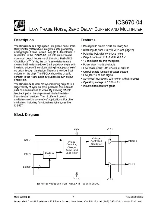
ICS670-02 L OW P HASE N OISE, Z ERO D ELAY B UFFER AND M ULTIPLIERDescriptionThe ICS670-02 is a high speed, low phase noise, Zero Delay Buffer (ZDB) which integrates ICS’ proprietary analog/digital Phase Locked Loop (PLL) techniques. Part of ICS’ ClockBlocks TM family, the part’s zero delay feature means that the rising edge of the input clock aligns with the rising edges of the outputs giving the appearance of no delay through the device. There are two identical outputs on the chip. The FBCLK should be used to connect to the FBIN. Each output has its own output enable pin.The ICS670-02 is ideal for synchronizing outputs in a large variety of systems, from personal computers to data communications to video. By allowing off-chip feedback paths, the chip can eliminate the delay through other devices. The 15 different on-chip multipliers work in a variety of applications. For other multipliers, including functional multipliers, see the ICS527.Features•Packaged in 16-pin SOIC•Available in Pb (lead) free package•Clock inputs from 5 to 160 MHz (see page 2)•Patented PLL with low phase noise•Output clocks up to 160 MHz at 3.3 V•15 selectable on-chip multipliers•Power down mode available•Low phase noise: -111 dBc/Hz at 10 kHz •Output enable function tri-states outputs•Low jitter 15 ps one sigma•Advanced, low power, sub-micron CMOS process •Operating voltage of 3.3 V or 5 VBlock DiagramL OW P HASE N OISE , Z ERO D ELAY B UFFER AND M ULTIPLIERPin AssignmentMultiplier Select TablePin DescriptionsS3S2S1S0CLK2 (and FBCLK)Input Range (MHz)0000Low (Power down entire chip)-0001Input x1.33318 - 1200010Input x6 5 - 26.670011Input x1.516.67 - 1070100Input x3.3337.5 - 480101Input x2.5010 - 640110Input x4 6 - 400111Input x125 - 1601000Input x2.33311 - 691001Input x2.66610 - 601010Input x12 5 - 13.331011Input x38 - 53.331100Input x10 5 - 161101Input x5 6 - 321110Input x8 5 - 201111Input x212 - 80Pin Number Pin Name Pin Type Pin Description1 - 3VDD InputPower supply. Connect both pins to the same voltage (either 3.3 V or 5 V).4CLK2Output Clock output from VCO. Output frequency equals the input frequency timesmultiplier.5OE2InputOutput clock enable 2. Tri-states the clock 2 output when low.6FBCLK Output Clock output from VCO. Output frequency equals the input frequency timesmultiplier.7OE1Input Output clock enable 1. Tri-states the feedback clock output when low.8FBIN Input Feedback clock input.9ICLK Input Clock input. Connect to a 5 - 160 MHz clock.10S3Input Multiplier select pin 3. Determines outputs per table above. Internal pull-up.11S2Input Multiplier select pin 2. Determines outputs per table above. Internal pull-up.12S1Input Multiplier select pin 1. Determines outputs per table above. Internal pull-up.13S0Input Multiplier select pin 0. Determines outputs per table above. Internal pull-up.14 - 16GNDPowerConnect to ground.L OW P HASE N OISE , Z ERO D ELAY B UFFER AND M ULTIPLIERExternal ComponentsThe ICS670-02 requires a minimum number of external components for proper operation. Decoupling capacitors of 0.01mF should be connected between VDD and GND on pins 4 and 5, and VDD and GND on pins 13 and 12, as close to the device as possible. A series termination resistor of 33Ω may be used to each clock output pin to reduce reflections.Absolute Maximum RatingsStresses above the ratings listed below can cause permanent damage to the ICS670-02. These ratings, which are standard values for ICS commercially rated parts, are stress ratings only. Functional operation of the device at these or any other conditions above those indicated in the operational sections of thespecifications is not implied. Exposure to absolute maximum rating conditions for extended periods can affect product reliability. Electrical parameters are guaranteed only over the recommended operating temperature range.Recommended Operation ConditionsDC Electrical CharacteristicsVDD=3.3 V ±10%, Ambient temperature -40 to +85°C, unless stated otherwiseItemRatingSupply Voltage, VDD 7 VAll Inputs and Outputs-0.5 V to VDD+0.5 V Ambient Operating Temperature 0 to +70°C Storage Temperature -65 to +150°C Junction Temperature 150°C Soldering Temperature260°CParameterMin.Typ.Max.UnitsAmbient Operating Temperature0+70°C Power Supply Voltage (measured in respect to GND)+3.0+5.5VParameterSymbolConditions Min.Typ.Max.UnitsOperating Voltage VDD 3.0 5.5V Input High Voltage V IH 2V Input Low Voltage V IL 0.8V Output High Voltage V OH I OH = -12 mA 2.4V Output Low Voltage V OL I OL = 12 mA 0.4V Output High Voltage, CMOS levelV OH I OH = -4 mA VDD-0.4VOperating Supply CurrentIDDNo Load35mAL OW P HASE N OISE , Z ERO D ELAY B UFFER AND M ULTIPLIERAC Electrical CharacteristicsVDD = 3.3V ±10%, Ambient Temperature -40 to +85°C, unless stated otherwiseNote 1: Rising edge of ICLK compared with rising edge of CLK2, with FBCLK connected to FBIN, and 15 pF load on CLK2.Thermal CharacteristicsShort Circuit Current I OS Each output ±50mA Internal Pull-up Resistor R PU OE, select pins 200k ΩInput CapacitanceC INOE, select pins5pFParameterSymbolConditionsMin.Typ.Max.UnitsParameterSymbolConditionsMin.Typ.Max.UnitsInput Clock Frequency f IN See table on page 25160MHz Output Clock Frequency 160MHz Output Rise Time t OR 0.8 to 2.0 V, no load 1.5ns Output Fall Time t OF 2.0 to 0.8 V, no load 1.5ns Output Clock Duty Cycle t DCmeasured at VDD/2455055%Input to Output Skew Note 1±100ps Maximum Absolute Jitter short term ±45ps Maximum Jitterone sigma 15ps Phase Noise, relative to carrier, 125 MHz (x5)100 Hz offset -103dBc/Hz 1 kHz offset -117dBc/Hz 10 kHz -111dBc/Hz 200 kHz-88dBc/HzParameterSymbolConditionsMin.Typ.Max.UnitsThermal Resistance Junction to AmbientθJA Still air 120°C/W θJA 1 m/s air flow 115°C/W θJA 3 m/s air flow105°C/W Thermal Resistance Junction to CaseθJC58°C/WL OW P HASE N OISE , Z ERO D ELAY B UFFER AND M ULTIPLIERPhase Noise for 125 MHz output, 25 MHz clock input(VDD = 3.3 V)L OW P HASE N OISE , Z ERO D ELAY B UFFER AND M ULTIPLIERPackage Outline and Package Dimensions (16-pin SOIC, 150 Mil. Narrow Body)Package dimensions are kept current with JEDEC Publication No. 95Ordering InformationParts that are ordered with a "LF" suffix to the part number are the Pb-Free configuration and are RoHS compliant.While the information presented herein has been checked for both accuracy and reliability, Integrated Circuit Systems (ICS) assumes no responsibility for either its use or for the infringement of any patents or other rights of third parties, which would result from its use. No other circuits, patents, or licenses are implied. This product is intended for use in normal commercial applications. Any other applications such as those requiring extended temperature range, high reliability, or other extraordinary environmental requirements are not recommended without additional processing by ICS. ICS reserves the right to change any circuitry or specifications without notice. ICS does not authorize or warrant any ICS product for use in life support devices or critical medical instruments.Part / Order NumberMarkingShipping PackagingPackageTemperatureICS670M-02ICS670M-02Tubes 16-pin SOIC 0 to +70°C ICS670M-02T ICS670M-02Tape and Reel16-pin SOIC 0 to +70°C ICS670M-02LF 670M-02LF Tubes 16-pin SOIC 0 to +70°C ICS670M-02LFT670M-02LFTape and Reel16-pin SOIC0 to +70°C。