XP-143E XP243规格书
- 格式:pdf
- 大小:794.12 KB
- 文档页数:2


14.Hard Processor System I/O Pin MultiplexingThe Intel Agilex SoC has a total of 48 flexible I/O pins that are used for hard processor system (HPS) operation, external flash memories, and external peripheral communication. A pin multiplexing mechanism allows the SoC to use the flexible I/O pins in a wide range of configurations.Related InformationIntel Agilex Hard Processor System Technical Reference Manual Revision History on page 12For details on the document revision history of this chapter14.1. Features of the Intel Agilex HPS I/O BlockThe I/O block provides the following functionality and features:•Dedicated HPS I/O pins—48 pins available for HPS clock, external flash memories and peripherals.Note: The HPS also interfaces with an SDRAM memory controller . This interface is separate from the dedicated pins discussed in this chapter .•I/O multiplexing—Selects pins used by each HPS peripheral —Can expose HPS peripheral interfaces to FPGA logicNote: When routed to the FPGA, some HPS peripherals require additional pipeline support in the connected soft logic. Refer to the relevant HPS peripheral chapter for details.You configure I/O multiplexing when you instantiate the HPS component in Platform Designer.Related InformationExternal Memory Interface Handbook For details about memory I/O pins in the SoC hard memory controller , refer to the Functional Description - HPS Memory Controller chapter of the External Memory Interface Handbook .MNL-1100 | 2021.03.09Send FeedbackISO 9001:2015Registered14.2. Intel Agilex HPS I/O System IntegrationThe HPS I/O block consists of the following sub-blocks:•Dedicated pin multiplexers (MUXes) – MUXes for the dedicated I/O bank •FPGA access pin multiplexers – MUXes for HPS peripheral connections to the FPGA fabric •Register slave interface – Provides access to control registers, which allow the bootloader to initialize I/O pins and HPS peripheral interfaces at system startupRelated InformationIntel Agilex I/O Control Registers on page 18514.3. Functional Description of the HPS I/O14.3.1. I/O PinsThe HPS has 48 dedicated I/O pins. They are divided into four quadrants of 12 signals per quadrant. When you instantiate the HPS component in Platform Designer, you must assign one of the 48 pins as the HPS clock. You can then use the remaining dedicated I/O pins for other common peripherals.You can alternatively route most HPS peripherals (except USB) through the FPGA.Select this routing when you instantiate the HPS Component. For more information,refer to the Intel Agilex HPS Component Reference Manual .Note:When assigning an HPS peripheral to HPS dedicated pins, you must assign all peripheral I/O pins to the same quadrant, except for NANDx16, Trace, and GPIO.Note: Although the HPS dedicated I/O pins are configured through the control registers,software cannot reconfigure the pins after I/O configuration is complete. There is no support for dynamically changing the pin MUX selections for HPS dedicated I/O pins.Related Information•Booting and Configuration on page 512Details about the boot up process for the Intel Agilex HPS •FPGA Access on page 184Information about routing HPS peripheral interfaces to the FPGA •Configuring HPS I/O Multiplexing on page 188Information about configuring the HPS I/O MUXes14.3.2. FPGA AccessMost HPS peripheral interfaces can be connected into the FPGA fabric, instead of to the dedicated I/O pins.HPS peripherals connect to the FPGA fabric through the FPGA access pin MUX. When connected to the FPGA fabric, peripheral interfaces are exposed as ports of the HPS component.14.Hard Processor System I/O Pin MultiplexingMNL-1100 | 2021.03.09Send FeedbackNote: For warm resets, software can set the brgwarmmask registers to prevent theassertion of module reset signals to peripheral modules.When a module that has been held in reset is ready to start running, software can deassert the respective reset signal by writing to the following appropriate register .Modules Module Reset Signal RegisterFPGA fabrics2f_rst -s2f_cold_rst -s2f_watchdog_rst-Debug domain with CoreSight and Trace dbg_rst_ndbgmodrst.dbg_rst dbgmodrst.csdap_rst MPU corereset_n [3:0]mpumodrst.core[3:0]cpuporreset_n [3:0]coldmodrst.cpupor[3:0]l2reset_n coldmodrst.l2DMA dma_rst_n per0modrst.dmadma_ecc_rst_n per0modrst.dmaocpdma_periph_if_rst_n [7:0]per0modrst.dmaif[7:0]SPI Master and Slave spim_rst_n [1:0]per0modrst.spim[1:0]spis_rst_n [1:0]per0modrst.spis[1:0]Ethernet MAC emac_rst_n [2:0]per0modrst.emac[2:0]emac_ecc_rst_n [2:0]per0modrst.emac[2:0]ocpemac_ptp_rst_n per0modrst.emacptpUSB usb_rst_n [1:0]b[1:0]usb_ecc_rst_n [1:0]b[1:0]ocpNAND Flash nand_flash_rst_n per0modrst.nandnand_flash_ecc_rst_n per0modrst.nandocpSD/MMC sdmmc_rst_n per0modrst.sdmmcsdmmc_ecc_rst_n per0modrst.sdmmcocpWatchdog watchdog_rst_n [3:0]per1modrst.watchdog[3:0]Timer l4sys_timer_rst_n [1:0]per1modrst.l4systimer[1:0]sp_timer_rst_n [1:0]per1modrst.sptimer[1:0]I 2C i2c_rst_n [4:0]per1modrst.i2c[4:0]UART uart_rst_n [1:0]per1modrst.uart[1:0]GPIO gpio_rst_n [1:0]per1modrst.gpio[1:0]SoC-to-FPGA Bridge soc2fpga_bridge_rst_n brgmodrst.soc2fpgaFPGA-to-SoC Bridge fpga2soc_bridge_rst_n brgmodrst.fpga2socLightweight SoC-to-FPGA Bridge lwsoc2fpga_bridge_rst_n brgmodrst.lwsoc2fpgaMPFE mpfe_rst_nbrgmodrst.mpfe 13.Reset ManagerMNL-1100 | 2021.03.09Send Feedback。


Table 180.Clock Manager Settings Register.FieldDescription en.emacptpenemac_ptp_clk output enable.en.emac0enen.emac1enen.emac2enEnables clock emac0_clk , emac1_clk and emac2_clk output.Note: There are corresponding ens and enr registers that allow the same fields to be set or cleared on a bit-by-bit basis.bypass.emacptp EMAC PTP clock bypass. This bit indicates if the emac_ptp_clk is bypassed to the input clockreference of the peripheral PLL.•0x0= No bypass occurs•0x1= emac_ptp_clk is bypassed to the input clock reference of the main PLL.Note: There are corresponding bypasss and bypassr registers that allow the same bits tobe set or cleared on a bit-by-bit basis.bypass.emacabypass.emacb Clock Bypass. This bit indicates whetheremaca_free_clk or emacb_free_clk is bypassed to the input clock reference of the main PLL.•0x0= No bypass occurs•0x1= emac*_free_clk is bypassed to the input clock reference of the main PLL.Note: There are corresponding bypasss and bypassr registers that allow the same bits tobe set or cleared on a bit-by-bit basis.emacctl.emac0selemacctl.emac1selemacctl.emac2sel EMAC clock source select. This bit selects the source for the emac*clk as either emaca_free_clk or emacb_free clk •0x0= emaca_free_clk •0x1=emacb_free_clk17.7.2. EMAC FPGA Interface InitializationTo initialize the Ethernet controller to use the FPGA GMII/MII interface, specific software steps must be followed.In general, the FPGA interface must be active in user mode with valid PHY clocks, the Ethernet Controller must be in a reset state during static configuration and the clock must be active and valid before the Ethernet Controller is brought out of reset.1.After the HPS is released from cold or warm reset, reset the Ethernet Controllermodule by setting the appropriate emac* bit in the per0modrst register in theReset Manager .2.Configure the EMAC Controller clock to 250 MHz by programming the appropriate registers in the Clock Manager .3.Bring the Ethernet PHY out of reset to verify that there are RX PHY clocks. For verification, you may have to coordinate with the bring up of transceiver from reset.4.If the PTP clock source is from the FPGA, ensure that the FPGAf2s_ptp_ref_clk is active.5.The soft GMII/MII adaptor must be loaded with active clocks propagating. The FPGA must be configured to user mode and a reset to the user soft FPGA IP may be required to propagate the PHY clocks to the HPS.6.Once all clock sources are valid, apply the following clock settings:a.Program the phy_intf_sel field of the emac* register in the SystemManager to 0x0 to select GMII/MII PHY interface.17.Ethernet Media Access ControllerMNL-1100 | 2021.03.09Send Feedbackb.If the PTP clock source is from the FPGA, set the ptp_clk_sel bit to 0x1 in the emac_global register of the System Manager .c.Enable the Ethernet Controller FPGA interface by setting the emac_* bit in the fpgaintf_en_3 register of the System Manager .7.Configure all of the EMAC static settings if the user requires a different setting from the default value. These settings include the AxPROT[1:0] and AxCACHEsignal values which are programmed in the emac* register of the System Manager .8.After confirming the settings are valid, software can clear the emac* bit in theper0modrst register of the Reset Manager to bring the EMAC out of reset..When these steps are completed, general Ethernet controller and DMA software initialization and configuration can continue.Note: These same steps can be applied to convert the HPS GMII to an RGMII, RMII or SGMII interface through the FPGA, except that in step 5 during FPGA configuration, you would load the appropriate soft adaptor for the interface and apply reset to it as well.The PHY interface select encoding would remain as 0x0. For the SGMII interface additional external transceiver logic would be required. Routing the Ethernet signals through the FPGA is useful for designs that are pin-limited in the HPS.17.7.3. EMAC HPS Interface InitializationTo initialize the Ethernet controller to use the HPS interface, specific software steps must be followed including selecting the correct PHY interface through the System Manager .In general, the Ethernet Controller must be in a reset state during static configuration and the clock must be active and valid before the Ethernet Controller is brought out of reset.1.After the HPS is released from cold or warm reset, reset the Ethernet Controllermodule by setting the appropriate emac* bit in the per0modrst register in theReset Manager .2.Configure the EMAC Controller clock to 250 MHz by programming the appropriate registers in the Clock Manager .3.Bring the Ethernet PHY out of reset to allow PHY to generate RX clocks.There are no registers to verify, but you can create the following custom logic block to cross check:•If the RX clock is routed through FPGA IO—you can use Signal Tap to check, or create a simple counter block with the RX clock as clock source to check if it runs.•If the RX clock is routed as HPS IO—you need to explore if the kernel application code is able to source through RX clock to check its status.4.When all the clocks are valid, program the following clock settings:a.Program the phy_intf_sel field of the emac* register in the SystemManager to 0x1 or 0x2 to select RGMII or RMII PHY interface.b.Disable the Ethernet Controller FPGA interface by clearing the emac_* bit inthe fpgaintf_en_3 register of the System Manager .17.Ethernet Media Access ControllerMNL-1100 | 2021.03.09Send Feedback5.Configure all of the EMAC static settings if the user requires a different setting from the default value. These settings include the AxPROT[1:0] and AxCACHEsignal values, which are programmed in the emac* register of the SystemManager .6.Execute a register read back to confirm the clock and static configuration settings are valid.7.After confirming the settings are valid, software can clear the emac* bit in theper0modrst register of the Reset Manager to bring the EMAC out of reset.When these steps are completed, general Ethernet controller and DMA software initialization and configuration can continue.17.7.4. DMA InitializationThis section provides the instructions for initializing the DMA registers in the proper sequence. This initialization sequence can be done after the EMAC interface initialization has been completed. Perform the following steps to initialize the DMA:1.Provide a software reset to reset all of the EMAC internal registers and logic. (DMA Register 0 (Bus Mode Register) – bit 0). †2.Wait for the completion of the reset process (poll bit 0 of the DMA Register 0 (Bus Mode Register), which is only cleared after the reset operation is completed). †3.Poll the bits of Register 11 (AXI Status) to confirm that all previously initiated (before software reset) or ongoing transactions are complete.Note: If the application cannot poll the register after soft reset (because of performance reasons), then it is recommended that you continue with the next steps and check this register again (as mentioned in step 12 on page 382)before triggering the DMA operations.†4.Program the following fields to initialize the Bus Mode Register by setting values in DMA Register 0 (Bus Mode Register):†•Mixed Burst and AAL •Fixed burst or undefined burst †•Burst length values and burst mode values †•Descriptor Length (only valid if Ring Mode is used)†5.Program the interface options in Register 10 (AXI Bus Mode Register). If fixed burst-length is enabled, then select the maximum burst-length possible on the bus (bits[7:1]).†6.Create a proper descriptor chain for transmit and receive. In addition, ensure that the receive descriptors are owned by DMA (bit 31 of descriptor should be set).When OSF mode is used, at least two descriptors are required.7.Make sure that your software creates three or more different transmit or receive descriptors in the chain before reusing any of the descriptors.†8.Initialize receive and transmit descriptor list address with the base address of the transmit and receive descriptor (Register 3 (Receive Descriptor List Address Register) and Register 4 (Transmit Descriptor List Address Register) respectively).†9.Program the following fields to initialize the mode of operation in Register 6(Operation Mode Register):17.Ethernet Media Access ControllerMNL-1100 | 2021.03.09Send Feedback。


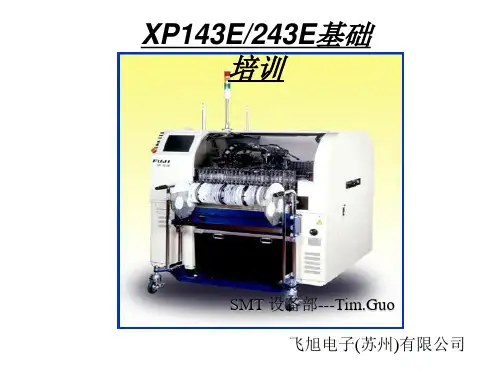
http://www.fuji.co.jp/Copyright © 2007 by Fuji Machine Manufacturing Co., Ltd. All Rights Reserved版本升级报告附加资料 No. 07031A发 行 日: 2007 年 8月 2日对 应 机 型: XP-143E/243E (后期机型) (控制软件)新 版 本 号: V1.51(已发行的版本号:V1.50)下页开始为版本升级报告 No.07031 的附加资料“XP 固有值一览 Type-III V1.51”的内容。
Fuji Machine Mfg.XP 固有値一覧 Type-III V1.512007-12-4現在XP固有值一览表Type-III V1.51//_/_/_/_/_/_/_/ Proper data /_未使用●XP启动时检查范围。
请必须设定在范围以内的值。
即使没有输入范围的记述,在整数型时-2147483648~2147483647,小数型时按整数的11位到小数点以下4位为止,字符串型到31个字符为止。
项目XP-143E XP243E输入范围测定值User编辑重新接通电源解说________MACHINE_TYPE_______=__xpMachineTypeA=121~3---否需要机种选择项目 XP14*:1 XP24*:2 XP34*:3__xpMachineTypeB=444---否需要机种选择项目 全机种:4 电路板搬运尺寸__xpMachineTypeC=331~3---否需要机种选择项目 TypeI:1 TypeII:2 TypeIII:3__xpMachineTypeD=11没有范围---否需要一般:1 批量机(1)和试验机(0)的区別,(区别使用的IO)__xpTI1200A=110~1---否1:相机TI-1200A__xpSetCVA1Cam=49610~255---否需要相机的设定(高分辨率相机建立与相机相对应的比特)第1比特:相机1第2比特:相机2第3比特:相机3第4比特:相机4第5比特: 将低分辨率相机作为HR-50处理第6比特: 将高分辨率相机作为G20U20处理第7比特: 将低分辨率相机作为XC-56处理__ServoPulseReduce=000~1---否0 : Pn201 = 16384 1 : Pn201 = 8192__DispMode=000~2---可XP141选择项目 0:影像处理中一切不显示 1:仅仅在覆盖式中显示 2:全部显示__CornerRearSide=220~2---否需要参照内侧的Corner Pattern进行补正处理的标记的指定 0:没有Corner Dog 1:Corner Dog __PanelReverseFlow=000~2---否电路板搬运方向的指定 0:左→右 1:右→左 (与FUJI标准机器同等) 2:右→左__RevolverInterLock=000~2---否需要增加了供料器浮起传感器和变更了吸嘴上升确认传感器 [T1.12e,T1.09h] 变更为0。

11.3.3. Hardware-Managed and Software-Managed ClocksWhen changing values on clocks, the terms hardware-managed and software-managed define how clock transitions are implemented. When changing a software-managed clock, software is responsible for gating off the clock, waiting for a PLL lock if required, and gating the clock back on. Clocks that are hardware-managed are automatically transitioned by the hardware to ensure glitch-free operation.The hardware-managed clocks are:•mpu_periph_clk •mpu_ccu_clk •mpu_clk •l3_main_free_clk •l4_sys_free_clk •l4_main_clk •l4_mp_clk •l4_sp_clk •cs_at_clk •cs_pdbg_clk •cs_trace_clkAll other clocks in the HPS are software-managed clocks.Note: During boot mode, all clocks are bypassed including both hardware-managed and software-managed clocks. Individual software bypasss controls are available for each set of clocks.11.3.4. Hardware Sequenced Clock GroupsThe hardware sequenced clock groups consists of the MPU clocks and the Interconnect clocks. The following diagram shows the external bypass muxes, hardware-managed external counters and dividers, and clock gates. For hardware-managed clocks, the group of clocks has only one software enable for the clock gate. As a result, the group of clocks are all enabled or disabled together . The slight exception is the Interconnect has five and MPU has two software enables.Table 85.Interconnect Clock Software Enables Software EnableAccess Descriptioncsclken RW Enables Debug clock output(cs_at_clk, cs_pdbg_clk,cs_trace_clk )l4spclken RW Enables clock l4_sp_clk outputl4mpclken RW Enables clock l4_mp_clk outputl4mainclken RWEnables clock l4_main_clk output 11.Clock ManagerMNL-1100 | 2021.03.09Send FeedbackTable 86.MPU Clock Software Enables Software Enable AccessDescription mpuclkenRW Enables mpu_clk , mpu_periph_clk ,and mpu_ccu_clk to MPU interface Figure 31.Hardware Clock Groupspll_main_c0pll_peri_c0HPS_OSC_CLKcb_intosc_div2_clkf2s_free_clk pll_main_c1pll_peri_c1HPS_OSC_CLKcb_intosc_div2_clkf2s_free_clk 11.Clock ManagerMNL-1100 | 2021.03.09Send FeedbackTable 87.The Hardware Sequenced Clocks Feature Summary Clock Output Group System Clock Name Frequency (18) value.Boot Frequency UsesMPU mpu_clk PLL C0boot_clk MPU systemcomplex,including CPU0-3mpu_ccu_clk mpu_clk /2boot_clk MPU level 2(L2) RAMmpu_periph_clk mpu_clk /4boot_clk MPUperipherals such as interrupts,timers, and watchdogInterconnect l3_main_free_clk PLL C1boot_clk L3interconnectl4_sys_free_clk l3_main_free_clk/{2,4}boot_clk /2L4interconnectl4_main_clkl3_main_free_clk /{1,2,4,8}boot_clk L4 main bus l4_mp_clkl3_main_free_clk /{1,2,4,8}boot_clk L4 MP bus l4_sp_clkl3_main_free_clk /{1,2,4,8}boot_clk/2L4 SP bus cs_at_clk l3_main_free_clk /{1,2,4,8}boot_clk CoreSightdebug trace buscs_pdbg_clk l3_main_free_clk /{1,4}boot_clk/2Debug AccessPort (DAP)and debug peripheral buscs_trace_clk l3_main_free_clk /{1,2,4,8}boot_clk/4CoreSightdebug trace port Interface Unit (TPIU)11.3.5. Software Sequenced ClocksThe software sequenced clock groups include additional clocks for peripherals not covered by the MPU and Interconnect clocks. The following diagram shows the external bypass muxes, hardware-managed external counters and dividers, and clock gates.(18)All clock frequencies must be less than the F max11.Clock ManagerMNL-1100 | 2021.03.09Send Feedback。
DatasheetHP EliteDisplay E24360.45cm(23.8")MonitorTake your mainstream display to the edgeStyle meets substance in astrikingly modern business displaycrafted for optimal viewing,productivity,and ergonomics.TheHP EliteDisplay E24360.45cm(23.8")Monitor has a3-sidedmicro-edge bezel for seamlessmulti-display tiling and4-wayadjustability so you cancomfortably power through yourday.Break the boundaries●Expand your productivity with uninterrupted views of one screen or many with a3-sided micro-edge bezel thatsupports virtually seamless arrays.1Get crisp visuals from any angle on the1920x1080Full HD resolution2,60.45cm(23.8")diagonal IPS screen.Work comfortably●Find your most comfortable,productive position with adjustable tilt,height,swivel,and up to150mm heightadjustment e pivot rotation to customize portrait or landscape views when using multiple displays.1Experience simple,convenient connectivity●Work with your most frequently-used devices with VGA,HDMI,and DisplayPort™.Connect your USB accessoriesright at the display with two USB3.0ports.Featuring●Create an efficient,compact solution when you mount your compatible HP Desktop Mini PC,Thin Client orChromebox directly on the column stand using the optional HP B300PC Mounting Bracket.3●Reduce power consumption and help lower costs with a low halogen,ENERGY STAR®certified,EPEAT®Goldregistered display that meets TCO Certified Edge with85%Post-Consumer Recycled plastics.4,5●Design the screen for how you work with HP Display Assistant software,which enables screen partitioning andhelps deter theft by dimming a display that’s disconnected without approval.●Build a complete solution with optional HP accessories like an HP Single Arm to take the display off the desk,anHP USB Graphics Adapter for multi-display setups or an HP S100Speaker Bar for space-saving audio.6HP EliteDisplay E24360.45cm(23.8")MonitorSpecifications TableProduct Number1FH47AA;Product Color Black and SilverDisplay size(diagonal)60.45cm(23.8")Display Type IPS w/LED backlightPanel Active Area52.7x29.64cm;Viewing Angle178°horizontal;178°verticalBrightness250cd/m²1Contrast Ratio1000:1static;10000000:1dynamic1Response Ratio5ms on/off1Aspect Ratio16:9Native Resolution FHD(1920x1080@60Hz)Resolutions Supported1920x1080;1680x1050;1600x900;1440x900;1280x1024;1280x800;1280x720;1024x768;800x600;720x400;640x480Display Features Anti-glare;BrightView Panel;In plane switching;Language selection;LED Backlights;On-screen controls;Pivot rotation;Plug and Play;Anti-static;Low HazeUser Controls Brightness;Color Control;Contrast;Exit;Image Control;Information;Input Control;Language;Management;Menu;Minus("-");OK;Plus("+");Power ControlInput signal1VGA;1HDMI1.4(with HDCP support);1DisplayPort™1.2(with HDCP support)Ports and Connectors3USB3.0(one upstream,two downstream)1Input power Input voltage:100to240VACPower consumption Energy Efficiency Class:A+;Panel Active Area:52.7x29.64cm;On-mode power consumption:18W;Annual energy consumption:26kWh;Power consumption(standby):0.5W;Power consumption(off-mode):0.3W;Power consumption Description:38W(maximum),21W(typical),0.5W(standby);Screen resolution:FHD(1920x1080@60Hz)53.88x20.49x33.29cmDimensions with Stand(W x Dx H)53.88x4.53x32.19cmDimensions without Stand(Wx D x H)Weight 5.59kg(With stand)Ergonomic features Tilt:-5to+20°;Swivel:±45°;Pivot rotation:90°;Height:150mmCertification and Compliance BSMI;CB;CCC;CE;CEL;cTUVus;ErP;FCC;ICES;ISC;ISO9241-307;Mexico CoC;MSIP;RCM;S-mark;SmartWay Transport Partnership-NA only;TUV-GS;VCCI;WEEEEnvironmental Arsenic-free display glass;Mercury-free display backlights;Low halogenEnergy Efficiency Compliance ENERGY STAR®certified;EPEAT®GoldWhat's in the box Monitor;AC power cord;VGA cable;USB cable(Type A male to Type B male);DisplayPort™1.2cable;CD(includes user guide,warranty,drivers);HP Display AssistantWarranty5years Next Business Day Onsite Support.HP support includes HP3-year limited warranty plus a5-year HP Onsite Care Pack support,as of date of purchase of the hardware product.Onsite support is offered if the problem cannot be handled over the phone.Delivery of support services outside of theapplicable HP coverage areas may be subject to longer response times.HP EliteDisplay E24360.45cm (23.8")MonitorAccessories and services (not included)HP B300PC MountingBracket Customize an altogether better solution with the HP B300PC Mounting Bracket,which lets you attach your HP Workstation,HP Desktop Mini,HP Chromebox or select HP Thin Client directly behind select 2017and 2018HP EliteDisplays and HP Z Displays.1Product number:2DW53AAHP S100Speaker Bar Add rich stereo audio to select 2017and 2018HP ProDisplays,HP EliteDisplays,and HP Z Displays 1without crowdingyour desk with the HP S100Speaker Bar ,which fits neatly underneath the display head and connects through USB.Product number:2LC49AAHP Single Monitor Arm The HP Single Monitor Arm is the perfect desk accessory for your work life.Sleek and streamlined,the HP Single MonitorArm is designed to complement the way you work.Product number:BT861AAHP Quick Release A secure and easy-to-use mounting solution for your VESA-compliant HP thin clients,compatible HP flat panel monitorsand other HP desktop products.Attach to any a compatible stand,bracket or wall mount and make the most of your workspace.Product number:EM870AAHP Integrated Work Centerfor Desktop Mini and Thin Client Make the most of small work spaces with an HP IWC Desktop Mini/Thin Client that lets you create a compact desktop solution by combining a display 1with an HP Desktop Mini,HP Thin Client or HP Chromebox 1and giving you convenient front access to all of its inputs.Product number:G1V61AAHP EliteDisplay E24360.45cm(23.8")MonitorMessaging Footnotes1Each display sold separately.2All performance specifications represent the typical specifications provided by HP's component manufacturers;actual performance may vary either higher or lower.3HP Desktop Mini PC,Thin Client,and Chromebox sold separately and require the HP B300PC Mounting Bracket,also sold separately.See display QuickSpecs for product compatibility.4External power supplies,power cords,cables and peripherals are not Low Halogen.Service parts obtained after purchase may not be Low Halogen.5EPEAT®registered where applicable.EPEAT registration varies by country.See for registration status by country.Search keyword generator on HP’s3rd party option store for solar generator accessories at /go/options6Each sold separately.Technical specifications disclaimers1All specifications represent the typical specifications provided by HP's component manufacturers,actual performance may vary either higher or lower.2External power supplies,power cords,cables and peripherals are not Low Halogen.Service parts obtained after purchase may not be Low Halogen.Sign up for updates/go/getupdated©Copyright2017HP Development Company,L.P.The information contained herein is subject to change without notice.The only warranties for HP productsand services are set forth in the express warranty statements accompanying such products and services.Nothing herein should be construed as constituting anadditional warranty.HP shall not be liable for technical or editorial errors or omissions contained herein.ENERGY STAR®and the ENERGY STAR®mark are registered trademarks of the U.S.Environmental Protection Agency.DisplayPort™and the DisplayPort™logoare trademarks owned by the Video Electronics Standards Association(VESA®)in the United States and other countries.4AA7-0720EE CH,November2017。
紧凑式高速贴片机规 格 说 明 书MODEL X P - 1 4 2 ECNT-XP142-01S富士机械制造株式会社FUJI MACHINE MFG.CO.,LTD.初版 '03 年9月目录1.概 要1.1概 要_______________________________________11.2特 长_______________________________________12.要素2.1要素___________________________________________2 3.机器规格3.1基本规格_____________________________________33.2电路板搬运____________________________________43.3对象电路板____________________________________44.机器构成4.1ON-THE-FLY-VISION___________________________54.2吸嘴的种类____________________________________64.3吸嘴配置_____________________________________74.4供料平台的构成_______________________________105.控制5.1控 制______________________________________116.选项6.1选项分类____________________________________126.2选项内容____________________________________137.机器外观7.1外观图______________________________________177.2电源和空气入口_______________________________18<注意>本机器的正式型号为「XP-142E」。
XP243E操作⼿册XP-243E TUT-XP243-1.0S XP-243E购⼊后如要转卖给第三⽅,请务必事先与本公司联系。
紧凑式⾼速贴⽚机XP-243E机械⼿册本机器的⼿册包含以下内容。
XP-243E操作⼿册XP-242E/243E系统⼿册XP-243E机械⼿册为了您能安全⾼效的使⽤本机器,请仔细阅读以上⼿册,并遵守上⾯记载的步骤及注意事项。
请将⼿册放在机器附近,以便使⽤时能⽴即浏览。
TUT-XP243-1.0S著作权本⼿册的著作权属于富⼠机械制造株式会社所有。
未经本公司同意,严禁擅⾃复制或转载本⼿册的部分或全部内容。
商标保证和责任本公司对由于下述原因⽽产⽣的结果不承担任何责任:·使⽤第三⽅零部件。
·使⽤⾮纯正FUJI零部件。
·⽤户的不正确设置。
·FUJI设备使⽤不当。
注意事项·本⼿册的内容在没有事先预告的情况下,有进⾏变更的可能性。
·本⼿册在编写过程中⼒求精益求精,如若发现错误之处敬请与本公司联系。
·本公司对因使⽤本⼿册所产⽣的结果及其所造成的影响,不承担任何责任。
TUT-XP243-1.0S本⼿册的有关事宜本⼿册的有关事宜本⼿册的构成本书是为了使操作者在使⽤机器的过程中学习其操作⽅法⽽编写的。
本书的构成和实际⽣产作业的顺序⼤致相同。
本书的内容只限于基本操作。
想得到更详细的资料,请参考 [XP-242E/243E 系统⼿册]和[XP-243E 机械⼿册]等⼿册。
第1章: 机器的构成⽤图解的⽅式来说明机器各个部分的名称。
第2章: 机器的启动和结束机器的启动和结束操作的说明。
第3章: ⽣产的准备⽣产程序的变更,各种模式的设定,重新贴装的设定等⽣产开始前的准备⼯作。
第4章: ⽣产的开始如何进⾏供料平台和料站位置确认等的说明。
第5章: 机器的停⽌各种机器停⽌⽅法的说明。
第6章: ⽣产的结束⽣产结束步骤的说明。
第7章: 保养归纳各个部位的⽇常保养,清扫的⼯作要领。
PXIe资料汇总一、物理结构PXIe国际规范的3U机箱母座物理接口中,PXI 联盟命名Peripheral Modules 为XJ3 和XJ4接口,相应公座称为XP3、XP4。
生产制造厂商中德国ENRI较多被使用,型号对应情况:XJ3 -> ENRI 973028 ;XJ4 -> ENRI 214443;XP3 -> ENRI 973027;XP4 -> ENRI 224057。
PXIe母座底面图PXIe母座侧面图二、接口定义2.1 概述根据PXI联盟定义3U 机箱中Peripheral Modules 的XJ3和XJ4硬件接口定义如下所示:2.2 XP3/XJ31PETp0~7/1PETn0~7/1PERp0~7/1PERn0~7数据差分线收发各八组[1],p56,CompactPCI Express中PET和PER命名规则与PCI Express相反,按外设板连接器为准,PET信号(如A5/B5)方向是从外设到系统,PER(如C5/D5)方向是从系统到外设。
电容耦合发生在发射侧[3],p64。
RefClk±100M差分时钟,该信号由backplane提供作为module的PCIe工作时钟。
该信号不是星型信号,各个slot间RefClk±相位不一致。
信号性质为LVPECL,可在外设侧电容耦合转换为其他电平[3],p80。
PERST#硬复位。
方向从slot到module,拉高表示PXI电源和参考时钟均已稳定[3],p99。
PRSNT#热插拔,低电平有效。
module接地处理。
PWREN#方向从系统到外设,一般用于开启外设版的主电源芯片,低电平有效。
此为短引脚,支持热插拔的外设可将该脚电阻上拉,在板卡插入过程的最后开启主电源[3],p107。
MPWRGD方向从外设到系统,表示外设电源已稳定,高电平有效。
支持热插拔的板卡,应将这个脚用10K电阻下拉到地,并接电源芯片PG脚[3],p108。