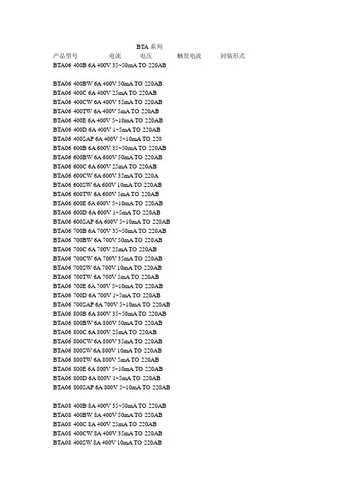
BTA20 CW中文资料
- 格式:pdf
- 大小:71.06 KB
- 文档页数:5
Symbol
Test Conditions
Quadrant
IGT
VD=12V (DC) RL=33Ω
VGT VGD
tgt
IL
VD=12V (DC) RL=33Ω
VD=VDRM RL=3.3kΩ
VD=VDRM IG = 500mA dIG/dt = 3A/µs
IG=1.2 IGT
Tj=25°C
Tj=25°C Tj=125°C Tj=25°C Tj=25°C
Non repetitive surge peak on-state current ( Tj initial = 25°C )
I2t value
tp = 8.3 ms tp = 10 ms tp = 10 ms
Critical rate of rise of on-state current Gate supply : IG = 500mA diG/dt = 1A/µs
700
800
400
600
700
800
March 1995
Unit A
A A2s A/µs
°C °C °C Unit
V
1/5
元器件交易网
BTA20 BW/CW / BTB20 BW/CW
THERMAL RESISTANCES
Symbol
Parameter
Value
Unit
Tj=125°C
* For either polarity of electrode A2 voltage with reference to electrode A1.
I-II-III
I-II-III I-II-III I-II-III
I-III II I-II-III
MIN MAX MAX MIN TYP
dissipation and maximum allowable temperatures (Tamb and Tcase) for different thermal resistances heatsink + contact (BTA).
Fig.3 : Correlation between maximum RMS power
IH *
VTM *
IDRM IRRM
IT= 500mA gate open
ITM= 28A tp= 380µs
VDRM Rated VRRM Rated
dV/dt * Linear slope up to VD=67%VDRM gate open
(dI/dt)c * Without snubber
Tj=25°C Tj=25°C Tj=25°C Tj=125°C Tj=125°C
Fig.9 : On-state characteristics (maximum values).
4/5
元器件交易网
PACKAGE MECHANICAL DATA TO220AB Plastic
A G
H J
I D B
O P
= N=
F L
C
M
Cooling method : C Marking : type number Weight : 2.3 g Recommended torque value : 0.8 m.N. Maximum torque value : 1 m.N.
BTB
2.1
°C/W
1.3
GATE CHARACTERISTICS (maximum values)
PG (AV) = 1W PGM = 10W (tp = 20 µs) IGM = 4A (tp = 20 µs)
ELECTRICAL CHARACTERISTICS
VGM = 16V (tp = 20 µs).
BW
CW
X
X
X
X
X
X
X
X
X
X
X
X
X
X
X
X
Fig.1 : Maximum RMS power dissipation versus RMS on-state current (F=50Hz). (Curves are cut off by (dI/dt)c limitation)
Fig.2 : Correlation between maximum RMS power
4.58 5.58 0.18 0.22
0.80 1.20 0.031 0.048
0.64 0.96 0.025 0.038
Information furnished is believed to be accurate and reliable. However, SGS-THOMSON Microelectronics assumes no responsability for the consequences of use of such information nor for any infringement of patents or other rights of third parties which may result from its use. No license is granted by implication or otherwise under any patent or patent rights of SGS-T HOMSON Microelectronics. Specifications mentioned in this publication are subject to change without notice. This publication supersedes and replaces all information previously supplied. SGS-THOMSON Microelectronics products are not authorized for use as critical components in life support devices or systems without express written approval of SGS-THOMSON Microelectronics.
Rth (j-a) Junction to ambient
60
°C/W
Rth (j-c) DC Junction to case for DC
BTA
2.8
°C/W
BTB
1.7
Rth (j-c) AC Junction to case for 360° conduction angle
BTA
( F= 50 Hz)
3/5
元器件交易网
BTA20 BW/CW / BTB20 BW/CW
Fig.5 : Relative variation of thermal impedance versus pulse duration.
Fig.6 : Relative variation of gate trigger current and holding current versus junction temperature.
Zth/Rth 1
Zt h( j-c)
0.1
Zt h(j-a)
0.01 1E-3
1E-2
1E-1
1E +0
tp( s) 1E+1 1E+2 5E+2
Fig.7 : Non Repetitive surge peak on-state current versus number of cycles.
Fig.8 : Non repetitive surge peak on-state current for a sinusoidal pulse with width : t ≤ 10ms, and corresponding value of I2t.
Repetitive F = 50 Hz
Non Repetitive
Storage and operating junction temperature range
Maximum lead temperature for soldering during 10 s at 4.5 mm from case
dissipation and maximum allowable temperatures (Tamb and Tcase) for different thermal resistances heatsink + contact (BTB).
Fig.4 : RMS on-state current versus case temperature.
INSULATING VOLTAGE = 2500V(RMS) (UL RECOGNIZED : E81734)
DESCRIPTION
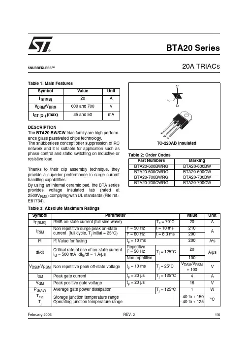
The BTA/BTB20 BW/CW triac family are high performance glass passivated chips technology. The SNUBBERLESS™ concept offer suppression of RC network and it is suitable for application such as phase control and static switching on inductive or resistive load.
5.85 6.85 0.230 0.270
4.50
0.178
2.54 3.00 0.100 0.119
4.48 4.82 0.176 0.190
3.55 4.00 0.140 0.158
1.15 1.39 0.045 0.055