Highest states in light-cone $AdS_5times S^5$ superstring
- 格式:pdf
- 大小:315.49 KB
- 文档页数:33


NuMicro®FamilyArm® ARM926EJ-S BasedNuMaker-HMI-N9H30User ManualEvaluation Board for NuMicro® N9H30 SeriesNUMAKER-HMI-N9H30 USER MANUALThe information described in this document is the exclusive intellectual property ofNuvoton Technology Corporation and shall not be reproduced without permission from Nuvoton.Nuvoton is providing this document only for reference purposes of NuMicro microcontroller andmicroprocessor based system design. Nuvoton assumes no responsibility for errors or omissions.All data and specifications are subject to change without notice.For additional information or questions, please contact: Nuvoton Technology Corporation.Table of Contents1OVERVIEW (5)1.1Features (7)1.1.1NuMaker-N9H30 Main Board Features (7)1.1.2NuDesign-TFT-LCD7 Extension Board Features (7)1.2Supporting Resources (8)2NUMAKER-HMI-N9H30 HARDWARE CONFIGURATION (9)2.1NuMaker-N9H30 Board - Front View (9)2.2NuMaker-N9H30 Board - Rear View (14)2.3NuDesign-TFT-LCD7 - Front View (20)2.4NuDesign-TFT-LCD7 - Rear View (21)2.5NuMaker-N9H30 and NuDesign-TFT-LCD7 PCB Placement (22)3NUMAKER-N9H30 AND NUDESIGN-TFT-LCD7 SCHEMATICS (24)3.1NuMaker-N9H30 - GPIO List Circuit (24)3.2NuMaker-N9H30 - System Block Circuit (25)3.3NuMaker-N9H30 - Power Circuit (26)3.4NuMaker-N9H30 - N9H30F61IEC Circuit (27)3.5NuMaker-N9H30 - Setting, ICE, RS-232_0, Key Circuit (28)NUMAKER-HMI-N9H30 USER MANUAL3.6NuMaker-N9H30 - Memory Circuit (29)3.7NuMaker-N9H30 - I2S, I2C_0, RS-485_6 Circuit (30)3.8NuMaker-N9H30 - RS-232_2 Circuit (31)3.9NuMaker-N9H30 - LCD Circuit (32)3.10NuMaker-N9H30 - CMOS Sensor, I2C_1, CAN_0 Circuit (33)3.11NuMaker-N9H30 - RMII_0_PF Circuit (34)3.12NuMaker-N9H30 - RMII_1_PE Circuit (35)3.13NuMaker-N9H30 - USB Circuit (36)3.14NuDesign-TFT-LCD7 - TFT-LCD7 Circuit (37)4REVISION HISTORY (38)List of FiguresFigure 1-1 Front View of NuMaker-HMI-N9H30 Evaluation Board (5)Figure 1-2 Rear View of NuMaker-HMI-N9H30 Evaluation Board (6)Figure 2-1 Front View of NuMaker-N9H30 Board (9)Figure 2-2 Rear View of NuMaker-N9H30 Board (14)Figure 2-3 Front View of NuDesign-TFT-LCD7 Board (20)Figure 2-4 Rear View of NuDesign-TFT-LCD7 Board (21)Figure 2-5 Front View of NuMaker-N9H30 PCB Placement (22)Figure 2-6 Rear View of NuMaker-N9H30 PCB Placement (22)Figure 2-7 Front View of NuDesign-TFT-LCD7 PCB Placement (23)Figure 2-8 Rear View of NuDesign-TFT-LCD7 PCB Placement (23)Figure 3-1 GPIO List Circuit (24)Figure 3-2 System Block Circuit (25)Figure 3-3 Power Circuit (26)Figure 3-4 N9H30F61IEC Circuit (27)Figure 3-5 Setting, ICE, RS-232_0, Key Circuit (28)Figure 3-6 Memory Circuit (29)Figure 3-7 I2S, I2C_0, RS-486_6 Circuit (30)Figure 3-8 RS-232_2 Circuit (31)Figure 3-9 LCD Circuit (32)NUMAKER-HMI-N9H30 USER MANUAL Figure 3-10 CMOS Sensor, I2C_1, CAN_0 Circuit (33)Figure 3-11 RMII_0_PF Circuit (34)Figure 3-12 RMII_1_PE Circuit (35)Figure 3-13 USB Circuit (36)Figure 3-14 TFT-LCD7 Circuit (37)List of TablesTable 2-1 LCD Panel Combination Connector (CON8) Pin Function (11)Table 2-2 Three Sets of Indication LED Functions (12)Table 2-3 Six Sets of User SW, Key Matrix Functions (12)Table 2-4 CMOS Sensor Connector (CON10) Function (13)Table 2-5 JTAG ICE Interface (J2) Function (14)Table 2-6 Expand Port (CON7) Function (16)Table 2-7 UART0 (J3) Function (16)Table 2-8 UART2 (J6) Function (16)Table 2-9 RS-485_6 (SW6~8) Function (17)Table 2-10 Power on Setting (SW4) Function (17)Table 2-11 Power on Setting (S2) Function (17)Table 2-12 Power on Setting (S3) Function (17)Table 2-13 Power on Setting (S4) Function (17)Table 2-14 Power on Setting (S5) Function (17)Table 2-15 Power on Setting (S7/S6) Function (18)Table 2-16 Power on Setting (S9/S8) Function (18)Table 2-17 CMOS Sensor Connector (CON9) Function (19)Table 2-18 CAN_0 (SW9~10) Function (19)NUMAKER-HMI-N9H30 USER MANUAL1 OVERVIEWThe NuMaker-HMI-N9H30 is an evaluation board for GUI application development. The NuMaker-HMI-N9H30 consists of two parts: a NuMaker-N9H30 main board and a NuDesign-TFT-LCD7 extensionboard. The NuMaker-HMI-N9H30 is designed for project evaluation, prototype development andvalidation with HMI (Human Machine Interface) function.The NuMaker-HMI-N9H30 integrates touchscreen display, voice input/output, rich serial port serviceand I/O interface, providing multiple external storage methods.The NuDesign-TFT-LCD7 can be plugged into the main board via the DIN_32x2 extension connector.The NuDesign-TFT-LCD7 includes one 7” LCD which the resolution is 800x480 with RGB-24bits andembedded the 4-wires resistive type touch panel.Figure 1-1 Front View of NuMaker-HMI-N9H30 Evaluation BoardNUMAKER-HMI-N9H30 USER MANUAL Figure 1-2 Rear View of NuMaker-HMI-N9H30 Evaluation Board1.1 Features1.1.1 NuMaker-N9H30 Main Board Features●N9H30F61IEC chip: LQFP216 pin MCP package with DDR (64 MB)●SPI Flash using W25Q256JVEQ (32 MB) booting with quad mode or storage memory●NAND Flash using W29N01HVSINA (128 MB) booting or storage memory●One Micro-SD/TF card slot served either as a SD memory card for data storage or SDIO(Wi-Fi) device●Two sets of COM ports:–One DB9 RS-232 port with UART_0 used 75C3232E transceiver chip can be servedfor function debug and system development.–One DB9 RS-232 port with UART_2 used 75C3232E transceiver chip for userapplication●22 GPIO expansion ports, including seven sets of UART functions●JTAG interface provided for software development●Microphone input and Earphone/Speaker output with 24-bit stereo audio codec(NAU88C22) for I2S interfaces●Six sets of user-configurable push button keys●Three sets of LEDs for status indication●Provides SN65HVD230 transceiver chip for CAN bus communication●Provides MAX3485 transceiver chip for RS-485 device connection●One buzzer device for program applicationNUMAKER-HMI-N9H30 USER MANUAL●Two sets of RJ45 ports with Ethernet 10/100 Mbps MAC used IP101GR PHY chip●USB_0 that can be used as Device/HOST and USB_1 that can be used as HOSTsupports pen drives, keyboards, mouse and printers●Provides over-voltage and over current protection used APL3211A chip●Retain RTC battery socket for CR2032 type and ADC0 detect battery voltage●System power could be supplied by DC-5V adaptor or USB VBUS1.1.2 NuDesign-TFT-LCD7 Extension Board Features●7” resolution 800x480 4-wire resistive touch panel for 24-bits RGB888 interface●DIN_32x2 extension connector1.2 Supporting ResourcesFor sample codes and introduction about NuMaker-N9H30, please refer to N9H30 BSP:https:///products/gui-solution/gui-platform/numaker-hmi-n9h30/?group=Software&tab=2Visit NuForum for further discussion about the NuMaker-HMI-N9H30:/viewforum.php?f=31 NUMAKER-HMI-N9H30 USER MANUALNUMAKER-HMI-N9H30 USER MANUAL2 NUMAKER-HMI-N9H30 HARDWARE CONFIGURATION2.1 NuMaker-N9H30 Board - Front View Combination Connector (CON8)6 set User SWs (K1~6)3set Indication LEDs (LED1~3)Power Supply Switch (SW_POWER1)Audio Codec(U10)Microphone(M1)NAND Flash(U9)RS-232 Transceiver(U6, U12)RS-485 Transceiver(U11)CAN Transceiver (U13)Figure 2-1 Front View of NuMaker-N9H30 BoardFigure 2-1 shows the main components and connectors from the front side of NuMaker-N9H30 board. The following lists components and connectors from the front view:NuMaker-N9H30 board and NuDesign-TFT-LCD7 board combination connector (CON8). This panel connector supports 4-/5-wire resistive touch or capacitance touch panel for 24-bits RGB888 interface.Connector GPIO pin of N9H30 FunctionCON8.1 - Power 3.3VCON8.2 - Power 3.3VCON8.3 GPD7 LCD_CSCON8.4 GPH3 LCD_BLENCON8.5 GPG9 LCD_DENCON8.7 GPG7 LCD_HSYNCCON8.8 GPG6 LCD_CLKCON8.9 GPD15 LCD_D23(R7)CON8.10 GPD14 LCD_D22(R6)CON8.11 GPD13 LCD_D21(R5)CON8.12 GPD12 LCD_D20(R4)CON8.13 GPD11 LCD_D19(R3)CON8.14 GPD10 LCD_D18(R2)CON8.15 GPD9 LCD_D17(R1)CON8.16 GPD8 LCD_D16(R0)CON8.17 GPA15 LCD_D15(G7)CON8.18 GPA14 LCD_D14(G6)CON8.19 GPA13 LCD_D13(G5)CON8.20 GPA12 LCD_D12(G4)CON8.21 GPA11 LCD_D11(G3)CON8.22 GPA10 LCD_D10(G2)CON8.23 GPA9 LCD_D9(G1) NUMAKER-HMI-N9H30 USER MANUALCON8.24 GPA8 LCD_D8(G0)CON8.25 GPA7 LCD_D7(B7)CON8.26 GPA6 LCD_D6(B6)CON8.27 GPA5 LCD_D5(B5)CON8.28 GPA4 LCD_D4(B4)CON8.29 GPA3 LCD_D3(B3)CON8.30 GPA2 LCD_D2(B2)CON8.31 GPA1 LCD_D1(B1)CON8.32 GPA0 LCD_D0(B0)CON8.33 - -CON8.34 - -CON8.35 - -CON8.36 - -CON8.37 GPB2 LCD_PWMCON8.39 - VSSCON8.40 - VSSCON8.41 ADC7 XPCON8.42 ADC3 VsenCON8.43 ADC6 XMCON8.44 ADC4 YMCON8.45 - -CON8.46 ADC5 YPCON8.47 - VSSCON8.48 - VSSCON8.49 GPG0 I2C0_CCON8.50 GPG1 I2C0_DCON8.51 GPG5 TOUCH_INTCON8.52 - -CON8.53 - -CON8.54 - -CON8.55 - -NUMAKER-HMI-N9H30 USER MANUAL CON8.56 - -CON8.57 - -CON8.58 - -CON8.59 - VSSCON8.60 - VSSCON8.61 - -CON8.62 - -CON8.63 - Power 5VCON8.64 - Power 5VTable 2-1 LCD Panel Combination Connector (CON8) Pin Function●Power supply switch (SW_POWER1): System will be powered on if the SW_POWER1button is pressed●Three sets of indication LEDs:LED Color DescriptionsLED1 Red The system power will beterminated and LED1 lightingwhen the input voltage exceeds5.7V or the current exceeds 2A.LED2 Green Power normal state.LED3 Green Controlled by GPH2 pin Table 2-2 Three Sets of Indication LED Functions●Six sets of user SW, Key Matrix for user definitionKey GPIO pin of N9H30 FunctionK1 GPF10 Row0 GPB4 Col0K2 GPF10 Row0 GPB5 Col1K3 GPE15 Row1 GPB4 Col0K4 GPE15 Row1 GPB5 Col1K5 GPE14 Row2 GPB4 Col0K6GPE14 Row2GPB5 Col1 Table 2-3 Six Sets of User SW, Key Matrix Functions●NAND Flash (128 MB) with Winbond W29N01HVS1NA (U9)●Microphone (M1): Through Nuvoton NAU88C22 chip sound input●Audio CODEC chip (U10): Nuvoton NAU88C22 chip connected to N9H30 using I2Sinterface–SW6/SW7/SW8: 1-2 short for RS-485_6 function and connected to 2P terminal (CON5and J5)–SW6/SW7/SW8: 2-3 short for I2S function and connected to NAU88C22 (U10).●CMOS Sensor connector (CON10, SW9~10)–SW9~10: 1-2 short for CAN_0 function and connected to 2P terminal (CON11)–SW9~10: 2-3 short for CMOS sensor function and connected to CMOS sensorconnector (CON10)Connector GPIO pin of N9H30 FunctionCON10.1 - VSSCON10.2 - VSSNUMAKER-HMI-N9H30 USER MANUALCON10.3 - Power 3.3VCON10.4 - Power 3.3VCON10.5 - -CON10.6 - -CON10.7 GPI4 S_PCLKCON10.8 GPI3 S_CLKCON10.9 GPI8 S_D0CON10.10 GPI9 S_D1CON10.11 GPI10 S_D2CON10.12 GPI11 S_D3CON10.13 GPI12 S_D4CON10.14 GPI13 S_D5CON10.15 GPI14 S_D6CON10.16 GPI15 S_D7CON10.17 GPI6 S_VSYNCCON10.18 GPI5 S_HSYNCCON10.19 GPI0 S_PWDNNUMAKER-HMI-N9H30 USER MANUAL CON10.20 GPI7 S_nRSTCON10.21 GPG2 I2C1_CCON10.22 GPG3 I2C1_DCON10.23 - VSSCON10.24 - VSSTable 2-4 CMOS Sensor Connector (CON10) FunctionNUMAKER-HMI-N9H30 USER MANUAL2.2NuMaker-N9H30 Board - Rear View5V In (CON1)RS-232 DB9 (CON2,CON6)Expand Port (CON7)Speaker Output (J4)Earphone Output (CON4)Buzzer (BZ1)System ResetSW (SW5)SPI Flash (U7,U8)JTAG ICE (J2)Power ProtectionIC (U1)N9H30F61IEC (U5)Micro SD Slot (CON3)RJ45 (CON12, CON13)USB1 HOST (CON15)USB0 Device/Host (CON14)CAN_0 Terminal (CON11)CMOS Sensor Connector (CON9)Power On Setting(SW4, S2~S9)RS-485_6 Terminal (CON5)RTC Battery(BT1)RMII PHY (U14,U16)Figure 2-2 Rear View of NuMaker-N9H30 BoardFigure 2-2 shows the main components and connectors from the rear side of NuMaker-N9H30 board. The following lists components and connectors from the rear view:● +5V In (CON1): Power adaptor 5V input ●JTAG ICE interface (J2) ConnectorGPIO pin of N9H30Function J2.1 - Power 3.3V J2.2 GPJ4 nTRST J2.3 GPJ2 TDI J2.4 GPJ1 TMS J2.5 GPJ0 TCK J2.6 - VSS J2.7 GPJ3 TD0 J2.8-RESETTable 2-5 JTAG ICE Interface (J2) Function●SPI Flash (32 MB) with Winbond W25Q256JVEQ (U7); only one (U7 or U8) SPI Flashcan be used●System Reset (SW5): System will be reset if the SW5 button is pressed●Buzzer (BZ1): Control by GPB3 pin of N9H30●Speaker output (J4): Through the NAU88C22 chip sound output●Earphone output (CON4): Through the NAU88C22 chip sound output●Expand port for user use (CON7):Connector GPIO pin of N9H30 FunctionCON7.1 - Power 3.3VCON7.2 - Power 3.3VCON7.3 GPE12 UART3_TXDCON7.4 GPH4 UART1_TXDCON7.5 GPE13 UART3_RXDCON7.6 GPH5 UART1_RXDCON7.7 GPB0 UART5_TXDCON7.8 GPH6 UART1_RTSCON7.9 GPB1 UART5_RXDCON7.10 GPH7 UART1_CTSCON7.11 GPI1 UART7_TXDNUMAKER-HMI-N9H30 USER MANUAL CON7.12 GPH8 UART4_TXDCON7.13 GPI2 UART7_RXDCON7.14 GPH9 UART4_RXDCON7.15 - -CON7.16 GPH10 UART4_RTSCON7.17 - -CON7.18 GPH11 UART4_CTSCON7.19 - VSSCON7.20 - VSSCON7.21 GPB12 UART10_TXDCON7.22 GPH12 UART8_TXDCON7.23 GPB13 UART10_RXDCON7.24 GPH13 UART8_RXDCON7.25 GPB14 UART10_RTSCON7.26 GPH14 UART8_RTSCON7.27 GPB15 UART10_CTSCON7.28 GPH15 UART8_CTSCON7.29 - Power 5VCON7.30 - Power 5VTable 2-6 Expand Port (CON7) Function●UART0 selection (CON2, J3):–RS-232_0 function and connected to DB9 female (CON2) for debug message output.–GPE0/GPE1 connected to 2P terminal (J3).Connector GPIO pin of N9H30 Function J3.1 GPE1 UART0_RXDJ3.2 GPE0 UART0_TXDTable 2-7 UART0 (J3) Function●UART2 selection (CON6, J6):–RS-232_2 function and connected to DB9 female (CON6) for debug message output –GPF11~14 connected to 4P terminal (J6)Connector GPIO pin of N9H30 Function J6.1 GPF11 UART2_TXDJ6.2 GPF12 UART2_RXDJ6.3 GPF13 UART2_RTSJ6.4 GPF14 UART2_CTSTable 2-8 UART2 (J6) Function●RS-485_6 selection (CON5, J5, SW6~8):–SW6~8: 1-2 short for RS-485_6 function and connected to 2P terminal (CON5 and J5) –SW6~8: 2-3 short for I2S function and connected to NAU88C22 (U10)Connector GPIO pin of N9H30 FunctionSW6:1-2 shortGPG11 RS-485_6_DISW6:2-3 short I2S_DOSW7:1-2 shortGPG12 RS-485_6_ROSW7:2-3 short I2S_DISW8:1-2 shortGPG13 RS-485_6_ENBSW8:2-3 short I2S_BCLKNUMAKER-HMI-N9H30 USER MANUALTable 2-9 RS-485_6 (SW6~8) FunctionPower on setting (SW4, S2~9).SW State FunctionSW4.2/SW4.1 ON/ON Boot from USB SW4.2/SW4.1 ON/OFF Boot from eMMC SW4.2/SW4.1 OFF/ON Boot from NAND Flash SW4.2/SW4.1 OFF/OFF Boot from SPI Flash Table 2-10 Power on Setting (SW4) FunctionSW State FunctionS2 Short System clock from 12MHzcrystalS2 Open System clock from UPLL output Table 2-11 Power on Setting (S2) FunctionSW State FunctionS3 Short Watchdog Timer OFFS3 Open Watchdog Timer ON Table 2-12 Power on Setting (S3) FunctionSW State FunctionS4 Short GPJ[4:0] used as GPIO pinS4Open GPJ[4:0] used as JTAG ICEinterfaceTable 2-13 Power on Setting (S4) FunctionSW State FunctionS5 Short UART0 debug message ONS5 Open UART0 debug message OFFTable 2-14 Power on Setting (S5) FunctionSW State FunctionS7/S6 Short/Short NAND Flash page size 2KBS7/S6 Short/Open NAND Flash page size 4KBS7/S6 Open/Short NAND Flash page size 8KBNUMAKER-HMI-N9H30 USER MANUALS7/S6 Open/Open IgnoreTable 2-15 Power on Setting (S7/S6) FunctionSW State FunctionS9/S8 Short/Short NAND Flash ECC type BCH T12S9/S8 Short/Open NAND Flash ECC type BCH T15S9/S8 Open/Short NAND Flash ECC type BCH T24S9/S8 Open/Open IgnoreTable 2-16 Power on Setting (S9/S8) FunctionCMOS Sensor connector (CON9, SW9~10)–SW9~10: 1-2 short for CAN_0 function and connected to 2P terminal (CON11).–SW9~10: 2-3 short for CMOS sensor function and connected to CMOS sensorconnector (CON9).Connector GPIO pin of N9H30 FunctionCON9.1 - VSSCON9.2 - VSSCON9.3 - Power 3.3VCON9.4 - Power 3.3V NUMAKER-HMI-N9H30 USER MANUALCON9.5 - -CON9.6 - -CON9.7 GPI4 S_PCLKCON9.8 GPI3 S_CLKCON9.9 GPI8 S_D0CON9.10 GPI9 S_D1CON9.11 GPI10 S_D2CON9.12 GPI11 S_D3CON9.13 GPI12 S_D4CON9.14 GPI13 S_D5CON9.15 GPI14 S_D6CON9.16 GPI15 S_D7CON9.17 GPI6 S_VSYNCCON9.18 GPI5 S_HSYNCCON9.19 GPI0 S_PWDNCON9.20 GPI7 S_nRSTCON9.21 GPG2 I2C1_CCON9.22 GPG3 I2C1_DCON9.23 - VSSCON9.24 - VSSTable 2-17 CMOS Sensor Connector (CON9) Function●CAN_0 Selection (CON11, SW9~10):–SW9~10: 1-2 short for CAN_0 function and connected to 2P terminal (CON11) –SW9~10: 2-3 short for CMOS sensor function and connected to CMOS sensor connector (CON9, CON10)SW GPIO pin of N9H30 FunctionSW9:1-2 shortGPI3 CAN_0_RXDSW9:2-3 short S_CLKSW10:1-2 shortGPI4 CAN_0_TXDSW10:2-3 short S_PCLKTable 2-18 CAN_0 (SW9~10) Function●USB0 Device/HOST Micro-AB connector (CON14), where CON14 pin4 ID=1 is Device,ID=0 is HOST●USB1 for USB HOST with Type-A connector (CON15)●RJ45_0 connector with LED indicator (CON12), RMII PHY with IP101GR (U14)●RJ45_1 connector with LED indicator (CON13), RMII PHY with IP101GR (U16)●Micro-SD/TF card slot (CON3)●SOC CPU: Nuvoton N9H30F61IEC (U5)●Battery power for RTC 3.3V powered (BT1, J1), can detect voltage by ADC0●RTC power has 3 sources:–Share with 3.3V I/O power–Battery socket for CR2032 (BT1)–External connector (J1)●Board version 2.1NUMAKER-HMI-N9H30 USER MANUAL2.3 NuDesign-TFT-LCD7 -Front ViewFigure 2-3 Front View of NuDesign-TFT-LCD7 BoardFigure 2-3 shows the main components and connectors from the Front side of NuDesign-TFT-LCD7board.7” resolution 800x480 4-W resistive touch panel for 24-bits RGB888 interface2.4 NuDesign-TFT-LCD7 -Rear ViewFigure 2-4 Rear View of NuDesign-TFT-LCD7 BoardFigure 2-4 shows the main components and connectors from the rear side of NuDesign-TFT-LCD7board.NuMaker-N9H30 and NuDesign-TFT-LCD7 combination connector (CON1).NUMAKER-HMI-N9H30 USER MANUAL 2.5 NuMaker-N9H30 and NuDesign-TFT-LCD7 PCB PlacementFigure 2-5 Front View of NuMaker-N9H30 PCB PlacementFigure 2-6 Rear View of NuMaker-N9H30 PCB PlacementNUMAKER-HMI-N9H30 USER MANUALFigure 2-7 Front View of NuDesign-TFT-LCD7 PCB PlacementFigure 2-8 Rear View of NuDesign-TFT-LCD7 PCB Placement3 NUMAKER-N9H30 AND NUDESIGN-TFT-LCD7 SCHEMATICS3.1 NuMaker-N9H30 - GPIO List CircuitFigure 3-1 shows the N9H30F61IEC GPIO list circuit.Figure 3-1 GPIO List Circuit NUMAKER-HMI-N9H30 USER MANUAL3.2 NuMaker-N9H30 - System Block CircuitFigure 3-2 shows the System Block Circuit.NUMAKER-HMI-N9H30 USER MANUALFigure 3-2 System Block Circuit3.3 NuMaker-N9H30 - Power CircuitFigure 3-3 shows the Power Circuit.NUMAKER-HMI-N9H30 USER MANUALFigure 3-3 Power Circuit3.4 NuMaker-N9H30 - N9H30F61IEC CircuitFigure 3-4 shows the N9H30F61IEC Circuit.Figure 3-4 N9H30F61IEC CircuitNUMAKER-HMI-N9H30 USER MANUAL3.5 NuMaker-N9H30 - Setting, ICE, RS-232_0, Key CircuitFigure 3-5 shows the Setting, ICE, RS-232_0, Key Circuit.NUMAKER-HMI-N9H30 USER MANUALFigure 3-5 Setting, ICE, RS-232_0, Key Circuit3.6 NuMaker-N9H30 - Memory CircuitFigure 3-6 shows the Memory Circuit.NUMAKER-HMI-N9H30 USER MANUALFigure 3-6 Memory Circuit3.7 NuMaker-N9H30 - I2S, I2C_0, RS-485_6 CircuitFigure 3-7 shows the I2S, I2C_0, RS-486_6 Circuit.NUMAKER-HMI-N9H30 USER MANUALFigure 3-7 I2S, I2C_0, RS-486_6 Circuit3.8 NuMaker-N9H30 - RS-232_2 CircuitFigure 3-8 shows the RS-232_2 Circuit.NUMAKER-HMI-N9H30 USER MANUALFigure 3-8 RS-232_2 Circuit3.9 NuMaker-N9H30 - LCD CircuitFigure 3-9 shows the LCD Circuit.NUMAKER-HMI-N9H30 USER MANUALFigure 3-9 LCD Circuit3.10 NuMaker-N9H30 - CMOS Sensor, I2C_1, CAN_0 CircuitFigure 3-10 shows the CMOS Sensor,I2C_1, CAN_0 Circuit.NUMAKER-HMI-N9H30 USER MANUALFigure 3-10 CMOS Sensor, I2C_1, CAN_0 Circuit3.11 NuMaker-N9H30 - RMII_0_PF CircuitFigure 3-11 shows the RMII_0_RF Circuit.NUMAKER-HMI-N9H30 USER MANUALFigure 3-11 RMII_0_PF Circuit3.12 NuMaker-N9H30 - RMII_1_PE CircuitFigure 3-12 shows the RMII_1_PE Circuit.NUMAKER-HMI-N9H30 USER MANUALFigure 3-12 RMII_1_PE Circuit3.13 NuMaker-N9H30 - USB CircuitFigure 3-13 shows the USB Circuit.NUMAKER-HMI-N9H30 USER MANUALFigure 3-13 USB Circuit3.14 NuDesign-TFT-LCD7 - TFT-LCD7 CircuitFigure 3-14 shows the TFT-LCD7 Circuit.Figure 3-14 TFT-LCD7 CircuitNUMAKER-HMI-N9H30 USER MANUAL4 REVISION HISTORYDate Revision Description2022.03.24 1.00 Initial version NUMAKER-HMI-N9H30 USER MANUALNUMAKER-HMI-N9H30 USER MANUALImportant NoticeNuvoton Products are neither intended nor warranted for usage in systems or equipment, anymalfunction or failure of which may cause loss of human life, bodily injury or severe propertydamage. Such applications are deemed, “Insecure Usage”.Insecure usage includes, but is not limited to: equipment for surgical implementation, atomicenergy control instruments, airplane or spaceship instruments, the control or operation ofdynamic, brake or safety systems designed for vehicular use, traffic signal instruments, all typesof safety devices, and other applications intended to support or sustain life.All Insecure Usage shall be made at customer’s risk, and in the event that third parties lay claimsto Nuvoton as a result of customer’s Insecure Usage, custome r shall indemnify the damagesand liabilities thus incurred by Nuvoton.。

Property of Lite-On Only1. DescriptionThe LTR-553ALS-WA is an integrated low voltage I2C digital light sensor [ALS] and proximity sensor [PS] with built-in emitter, in a single miniature chipled lead-free surface mount package. This sensor converts light intensity to a digital output signal capable of direct I2C interface. It provides a linear response over a wide dynamic range from 0.01 lux to 64k lux and is well suited to applications under high ambient brightness. With built-in proximity sensor (emitter and detector), LTR-553ALS-WA offers the feature to detect object at a user configurable distance.The sensor supports an interrupt feature that removes the need to poll the sensor for a reading which improves system efficiency. The sensor also supports several features that help to minimize the occurrence of false triggering. This CMOS design and factory-set one time trimming capability ensure minimal sensor-to-sensor variations for ease of manufacturability to the end customers.2. Features∙I2C interface (Fast Mode @ 400kbit/s)∙Ultra-small ChipLED package∙Built-in temperature compensation circuit∙Low active power consumption with standby mode∙Supply voltage range from 2.4V to 3.6V capable of 1.7V logic voltage∙Operating temperature range from -30︒C to +70︒C∙RoHS and Halogen free compliant∙Light SensorClose to human eye spectral responseImmunity to IR / UV Light SourceAutomatically rejects 50 / 60 Hz lightings flicker6 dynamic range from 0.01 lux to 64k lux16-bit effective resolution∙Proximity SensorBuilt-in LED driver, emitter and detectorProgrammable LED drive settings11-bit effective resolutionHigh ambient light suppressionPart No.:LTR-553ALS-WA DATA SHEET Page: 1 of 41Property of Lite-On OnlyProperty of Lite-On Only5. Outline DimensionsNotes:1. All dimensions are in millimetersPart No.:LTR-553ALS-WA DATA SHEET Page: 3 of 41Property of Lite-On Only 6. Functional Block DiagramLTR-553ALSProperty of Lite-On Only LTR-553ALSProperty of Lite-On OnlyProperty of Lite-On OnlyProperty of Lite-On OnlyProperty of Lite-On Only2Property of Lite-On OnlyProperty of Lite-On OnlyProperty of Lite-On OnlyProperty of Lite-On OnlyProperty of Lite-On OnlyProperty of Lite-On OnlyProperty of Lite-On OnlyProperty of Lite-On OnlyProperty of Lite-On OnlyProperty of Lite-On OnlyProperty of Lite-On OnlyProperty of Lite-On OnlyProperty of Lite-On OnlyProperty of Lite-On OnlyProperty of Lite-On OnlyProperty of Lite-On OnlyProperty of Lite-On OnlyProperty of Lite-On OnlyProperty of Lite-On OnlyProperty of Lite-On OnlyProperty of Lite-On OnlyProperty of Lite-On OnlyProperty of Lite-On OnlyProperty of Lite-On Only11. Pseudo Codes ExamplesControl Registers// The Control Registers define the operating modes and gain settings of the ALS and PS of LTR-553.// Default settings are 0x00 for both registers (both in Standby mode).Slave_Addr = 0x23 // Slave address of LTR-553 device// Enable ALSRegister_Addr = 0x80 // ALS_CONTR registerCommand = 0x01 // For Gain X1// For Gain X2, Command = 0x05// For Gain X4, Command = 0x09// For Gain X8, Command = 0x0D// For Gain X48, Command = 0x19// For Gain X96, Command = 0x1DWriteByte(Slave_Addr, Register_Addr, Command)// Enable PSRegister_Addr = 0x81 // PS_CONTR registerCommand = 0x03 // Gain = 16// For Gain = 32, Command = 0x0B// For Gain = 64, Command = 0x0FWriteByte(Slave_Addr, Register_Addr, Command)PS LED Registers// The PS LED Registers define the LED pulse modulation frequency, duty cycle and peak current.// Default setting is 0x7F (60kHz, 100%, 100mA).Slave_Addr = 0x23 // Slave address of LTR-553 device// Set LED Pulse Freq 30kHz (duty cycle 100%, peak curr 100mA)Register_Addr = 0x82 // PS_LED registerCommand = 0x1F // Pulse Freq = 30kHz, (duty cyc 100%, peak curr 100mA)// For Pulse Freq = 40kHz, (100%, 100mA), Command = 0x3F// For Pulse Freq = 50kHz, (100%, 100mA), Command = 0x5F// For Pulse Freq = 60kHz, (100%, 100mA), Command = 0x7F// For Pulse Freq = 70kHz, (100%, 100mA), Command = 0x9F// For Pulse Freq = 80kHz, (100%, 100mA), Command = 0xBF// For Pulse Freq = 90kHz, (100%, 100mA), Command = 0xDF// For Pulse Freq = 100kHz, (100%, 100mA), Command = 0xFF WriteByte(Slave_Addr, Register_Addr, Command)// Set LED Duty Cycle 25% (pulse freq 60kHz, peak curr 100mA)Register_Addr = 0x82 // PS_LED registerCommand = 0x67 // Duty Cycle = 25%, (pulse freq 60kHz, peak curr 100mA)// For Duty Cycle = 50%, (60kHz, 100mA), Command = 0x6F// For Duty Cycle = 75%, (60kHz, 100mA), Command = 0x77// For Duty Cycle = 100%, (60kHz, 100mA), Command = 0x7F WriteByte(Slave_Addr, Register_Addr, Command)Part No.:LTR-553ALS-WA DATA SHEET Page: 33 of 41Property of Lite-On Only// Set LED Peak Current 5mA (pulse freq 60kHz, duty cycle 100%)Register_Addr = 0x82 // PS_LED registerCommand = 0x78 // Peak Current = 5mA, (pulse freq 60kHz, duty cyc 100%)// For Peak Current = 10mA, (60kHz, 100%), Command = 0x79// For Peak Current = 20mA, (60kHz, 100%), Command = 0x7A// For Peak Current = 50mA, (60kHz, 100%), Command = 0x7B WriteByte(Slave_Addr, Register_Addr, Command)PS Measurement Rate// The PS_MEAS_RATE register controls the PS measurement rate.// Default setting of the register is 0x02 (repeat rate 100ms)Slave_Addr = 0x23 // Slave address of LTR-553 device// Set PS Repeat Rate 50msRegister_Addr = 0x84 // PS_MEAS_RATE registerCommand = 0x00 // Meas rate = 50ms// For Meas rate = 500ms, Command = 0x04WriteByte(Slave_Addr, Register_Addr, Command)ALS Measurement Rate// The ALS_MEAS_RATE register controls the ALS integration time and measurement rate.// Default setting of the register is 0x03 (integration time 100ms, repeat rate 500ms)Slave_Addr = 0x23 // Slave address of LTR-553 device// Set ALS Integration Time 200ms, Repeat Rate 200msRegister_Addr = 0x85 // ALS_MEAS_RATE registerCommand = 0x12 // Int time = 200ms, Meas rate = 200ms// For Int time = 400ms, Meas rate = 500ms, Command = 0x1B WriteByte(Slave_Addr, Register_Addr, Command)ALS Data Registers (Read Only)// The ALS Data Registers contain the ADC output data for the respective channel.// These registers should be read as a group, with the lower address being read first.Slave_Addr = 0x23 // Slave address of LTR-553 device// Read back ALS_DATA_CH1Register_Addr = 0x88 // ALS_DATA_CH1 low byte addressReadByte(Slave_Addr, Register_Addr, Data0)Register_Addr = 0x89 // ALS_DATA_CH1 high byte addressReadByte(Slave_Addr, Register_Addr, Data1)// Read back ALS_DATA_CH0Register_Addr = 0x8A // ALS_DATA_CH0 low byte addressReadByte(Slave_Addr, Register_Addr, Data2)Register_Addr = 0x8B // ALS_DATA_CH0 high byte addressReadByte(Slave_Addr, Register_Addr, Data3)ALS_CH1_ADC_Data = (Data1 << 8) | Data0 // Combining lower and upper bytes to give 16-bit Ch1 dataALS_CH0_ADC_Data = (Data3 << 8) | Data2 // Combining lower and upper bytes to give 16-bit Ch0 dataPart No.:LTR-553ALS-WA DATA SHEET Page: 34 of 41Property of Lite-On OnlyALS / PS Status Register (Read Only)// The ALS_PS_STATUS Register contains the information on Interrupt, ALS and PS data availability status.// This register is read only.Slave_Addr = 0x23 // Slave address of LTR-553 device// Read back RegisterRegister_Addr = 0x8C // ALS_PS_STATUS register addressReadByte(Slave_Addr, Register_Addr, Data)Interrupt_Status = Data & 0x0A // Interrupt_Status = 8(decimal) → ALS Interrupt// Interrupt_Status = 2(decimal) → PS Interrupt// Interrupt_Status = 10(decimal) → Both InterruptNewData_Status = Data & 0x05 // NewData_Status = 4(decimal) → ALS New Data// NewData_Status = 1(decimal) → PS New Data// NewData_Status = 5(decimal) → Both New DataALS_Data_Valid = Data & 0x80 // ALS_Data_Valid = 0x00 → ALS New Data is valid (usable)// ALS_Data_Valid = 0x80 → ALS New Data is invalid, discard andwait for new ALS dataPS Data Registers (Read Only)// The PS Data Registers contain the ADC output data.// These registers should be read as a group, with the lower address being read first.Slave_Addr = 0x23 // Slave address of LTR-553 device// Read back PS_DATA registersRegister_Addr = 0x8D // PS_DATA low byte addressReadByte(Slave_Addr, Register_Addr, Data0)Register_Addr = 0x8E // PS_DATA high byte addressReadByte(Slave_Addr, Register_Addr, Data1)PS_ADC_Data = (Data1 << 8) | Data0 // Combining lower and upper bytes to give 16-bit PS data Interrupt Registers// The Interrupt register controls the operation of the interrupt pins and function.// The default value for this register is 0x08 (Interrupt inactive)Slave_Addr = 0x23 // Slave address of LTR-553 device// Set Interrupt Polarity for Active Low, both ALS and PS triggerRegister_Addr = 0x8F // Interrupt Register addressCommand = 0x03 // Interrupt is Active Low and both ALS and PS can trigger// For Active High Interrupt, both trigger, Command = 0x07// For Active High Interrupt, ONLY ALS trigger, Command = 0x06// For Active High Interrupt, ONLY PS trigger, Command = 0x05 WriteByte(Slave_Addr, Register_Addr, Command)Part No.:LTR-553ALS-WA DATA SHEET Page: 35 of 41Property of Lite-On OnlyALS Threshold Registers// The ALS_THRES_UP and ALS_THRES_LOW registers determines the upper and// lower limit of the interrupt threshold value.// Following example illustrates the setting of the ALS threshold window of// decimal values of 200 (lower threshold) and 1000 (upper threshold)Slave_Addr = 0x23 // Slave address of LTR-553 device// Upper Threshold Setting (decimal 1000)ALS_Upp_Threshold_Reg_0 = 0x97 // ALS Upper Threshold Low Byte Register addressALS_Upp_Threshold_Reg_1 = 0x98 // ALS Upper Threshold High Byte Register addressData1 = 1000 >> 8 // To convert decimal 1000 into two eight bytes register values Data0 = 1000 & 0xFFWriteByte(Slave_Addr, ALS_Upp_Threshold_Reg_0, Data0)WriteByte(Slave_Addr, ALS_Upp_Threshold_Reg_1, Data1)// Lower Threshold Setting (decimal 200)ALS_Low_Threshold_Reg_0 = 0x99 // ALS Lower Threshold Low Byte Register addressALS_Low_Threshold_Reg_1 = 0x9A // ALS Lower Threshold High Byte Register addressData1 = 200 >> 8 // To convert decimal 200 into two eight bytes register values Data0 = 200 & 0xFFWriteByte(Slave_Addr, ALS_Low_Threshold_Reg_0, Data0)WriteByte(Slave_Addr, ALS_Low_Threshold_Reg_1, Data1)PS Threshold Registers// The PS_THRES_UP and PS_THRES_LOW registers determines the upper and// lower limit of the interrupt threshold value.// Following example illustrates the setting of the PS threshold window of// decimal values of 200 (lower threshold) and 1000 (upper threshold)Slave_Addr = 0x23 // Slave address of LTR-553 device// Upper Threshold Setting (decimal 1000)PS_Upp_Threshold_Reg_0 = 0x90 // PS Upper Threshold Low Byte Register addressPS_Upp_Threshold_Reg_1 = 0x91 // PS Upper Threshold High Byte Register addressData1 = 1000 >> 8 // To convert decimal 1000 into two eight bytes register values Data0 = 1000 & 0xFFWriteByte(Slave_Addr, PS_Upp_Threshold_Reg_0, Data0)WriteByte(Slave_Addr, PS_Upp_Threshold_Reg_1, Data1)// Lower Threshold Setting (decimal 200)PS_Low_Threshold_Reg_0 = 0x92 // PS Lower Threshold Low Byte Register addressPS_Low_Threshold_Reg_1 = 0x93 // PS Lower Threshold High Byte Register addressData1 = 200 >> 8 // To convert decimal 200 into two eight bytes register values Data0 = 200 & 0xFFWriteByte(Slave_Addr, PS_Low_Threshold_Reg_0, Data0)WriteByte(Slave_Addr, PS_Low_Threshold_Reg_1, Data1)Part No.:LTR-553ALS-WA DATA SHEET Page: 36 of 41Property of Lite-On OnlyProperty of Lite-On OnlyProperty of Lite-On Only Recommended Land PatternProperty of Lite-On OnlyProperty of Lite-On OnlyPart No.: LTR-553ALS-WA DATA SHEETPage: 41 of 41BNS-OD-C131/A4 - Rev 1.0 – 22 May 201315. Package Dimension for Tape and ReelNote:1. All dimensions are in millimetersNotes:1. All dimensions are in millimeters (inches)2. Empty component pockets sealed with top cover tape3. 7 inch reel - 2500 pieces per reel4. In accordance with ANSI/EIA 481-1-A-1994 specifications。

Operator’s ManualEDACS® ALLEGRAVEHICLE HANDSFREE ericssonz2NOTICE!This manual covers Ericsson and General Electric products manufactured and sold byThis manual is published by Ericsson Inc., without any warranty. Improvements and changes to this manual necessitated by typographical errors, inaccu-racies of current information, or improvements to programs and/or equipment, may be made by Er-icsson Inc., at any time and without notice. Such changes will be incorporated into new editions of this manual. No part of this manual may be reproduced or transmitted in any form or by any means, elec-tronic or mechanical, including photocopying and recording, for any purpose, without the express writ-ten permission of Ericsson Inc.Copyright © February 1995, Ericsson Inc.VEHICLE HANDSFREE PACKAGEThe VEHICLE HANDSFREE Package lets you talk on a portable radio in your car without taking your hands off the wheel. Your radio operates as usual, except that you use an external microphone, speaker, and antenna.The HANDSFREE powers the radio and charges its battery (standard or slim-line only).USING YOUR HANDSFREE UNIT INSERTING THE RADIOBefore inserting the radio remove the following:• the round rubber plug in the antenna port on the back of the radio.• the system connector plug from the bottom of the radio.3INSERT THE RADIO INTO THE HANDSFREE HOLDER1. Slide the radio straight down parallel tothe back of the holder.2. Push the radio all the way down tomake sure the system connector is properly seated.3. Push the radio back until the side tabsof the handsfree unit lock into place.4OPERATING INSTRUCTIONS Service Available IndicatorThe indicator light on the top edge of the radio shows a steady green light when service is available from the service net-work.Answering A CallRefer to your radio user’s guide to se-lect an answering option. Most radios have at least three options:• answer with the SEND key• answer with any key except VOL-UME keys• answer automatically after a num-ber of rings Adjusting The Speaker VolumeWhen the radio is in the cradle and turned on, you can adjust the speaker vol-ume using the volume keys. The radio stores two volume settings independently--one for when the radio is used as a port-able, and one for the speaker volume when the radio is in the HANDSFREE unit. Both settings remain unchanged after the radio is turned off.CHARGING YOUR RADIO BATTERYWhen your radio is on and in standby mode in the HANDSFREE unit, the radio battery is automatically charged. You can charge your radio battery by leaving the phone in the cradle overnight. However, continuously charging the battery in this5way for more than a week can temporarily weaken the vehicle battery.• When your radio is in the HANDSFREE unit, the radio dis-play will indicate charge status. Theindicator alternates between C for“Charging” and the charge level (0through 9). When the battery isfully charged, the display shows an“F” for “Full Charge.”• The HANDSFREE unit recharges a standard battery in less than twohours and a similar battery in lessthan an hour.NOTE: Charging pauses when acall is in progress, but a tricklecharge maintains the batterycharge level.• To use your radio in the HANDSFREE unit if the radio bat-tery is completely discharged (i.e., the radio will not turn on), place the radio in the unit and wait 10 min-utes before placing a call.6REMOVING THE RADIO1. To release the radio from theHANDSFREE unit, squeeze the tabson both sides of the holder until theradio tilts slightly forward.2. Slide the radio straight up out of theholder so that the HANDSFREE sys-tem connector detaches from the baseof the phone.7CARE AND MAINTENANCE• Carefully follow the instructions on Inserting and Removing the radiofrom the HANDSFREE unit.• Do not attempt to service the HANDSFREE unit or componentsyourself. Doing so will void the war-ranty.• Follow all safety precautions and user guidelines8TROUBLESHOOTINGRADIO PROBLEM PROBABLE CAUSE REMEDYThe LED does not light when the vehicle power is supplied.The holder is not receivingpower, or vehicle power polar-ity is reversed.Check the power connec-tions and fuse. Be sure theradio battery is charged.The portable radio functions outside the holder, but not in the holder.Radio is not properly seated inthe holder, or the system con-nector contacts are dirty, or theexternal antenna is discon-nected or defective.Be sure the radio is properlyseated in the holder. If sys-tem connector contacts aredirty, carefully clean them.The other party of the radio connection cannot hear sound.The microphone jack is not in-serted into the connection box.Clean the microphone plugand insert it into the connec-tion box.No audio The speaker jack is notinserted into the connectionbox.Clean the speaker plug and insert it into the connection box.9NOTES 101112Ericsson Inc.Private Radio SystemsMountain View RoadLynchburg, Virginia 24502AE/LZT 123 1873 R1A 1-800-528-7711 (Outside USA, 804-528-7711)Printed in U.S.A.。

峰值亮度英语Peak luminancePeak luminance refers to the maximum brightness that a display or light source can achieve. It is an important specification for displays, especially for high dynamic range (HDR) content, as it directly impacts the perceived contrast and vividness of the images.In the context of displays, peak luminance is usually measured in units of nits, which is a measure of light output per unit area. A higher peak luminance means that the display can produce brighter highlights and more dazzling visuals, which is particularly important for HDR content that contains a wide range of brightness levels.In practical terms, a higher peak luminance allows for better representation of bright outdoor scenes, highlights in reflections, and other high-contrast elements in the image. This results in a more lifelike and immersive viewing experience, as the display can more accurately reproduce the dynamic range of the original content.For example, a display with a peak luminance of 1000nits will be able to render brighter highlights and more details in the brightest parts of the image compared to a display with a peak luminance of 500 nits. This can make a significant difference in the perceived image quality, especially when viewing HDR content with a wide range of brightness levels.In addition to displays, peak luminance is also acrucial factor for other light sources, such as projectors and LED lights. For projectors, a higher peak luminance allows for better visibility in well-lit environments and more impactful presentations or movie screenings. For LED lights, a higher peak luminance can enhance the overall brightness and clarity of the illuminated space.In summary, peak luminance is an important specification for displays, projectors, and other light sources, as it directly impacts the perceived brightness and contrast of the visuals. A higher peak luminance allows for better representation of highlights and a more immersive viewing experience, especially for HDR content.峰值亮度峰值亮度是指显示器或光源可以达到的最大亮度。
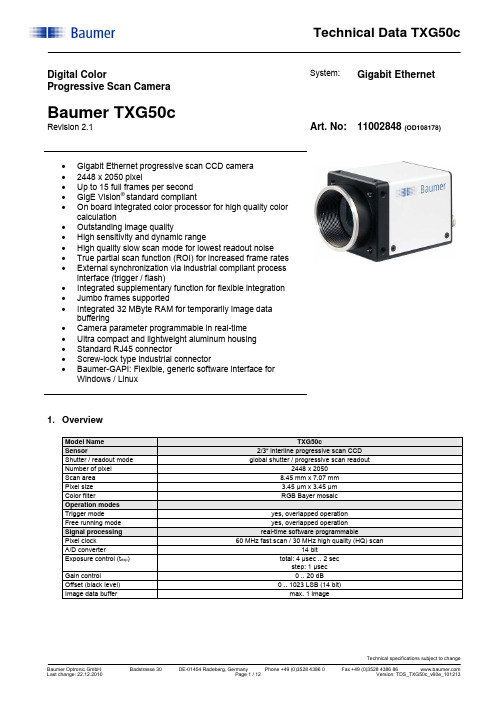
System: Gigabit Ethernet Digital ColorProgressive Scan CameraBaumer TXG50cRevision 2.1 Art. No: 11002848 (OD108178) Array•Gigabit Ethernet progressive scan CCD camera•2448 x 2050 pixel•Up to 15 full frames per second• GigE Vision® standard compliant•On board integrated color processor for high quality colorcalculation•Outstanding image quality•High sensitivity and dynamic range•High quality slow scan mode for lowest readout noise•True partial scan function (ROI) for increased frame rates•External synchronization via industrial compliant processinterface (trigger / flash)•Integrated supplementary function for flexible integration•Jumbo frames supported•Integrated 32 MByte RAM for temporarily image databuffering•Camera parameter programmable in real-time•Ultra compact and lightweight aluminum housing•Standard RJ45 connector•Screw-lock type industrial connector•Baumer-GAPI: Flexible, generic software interface forWindows / Linux1. OverviewModel Name TXG50cSensor 2/3“ interline progressive scan CCDShutter / readout mode global shutter / progressive scan readoutNumber of pixel 2448 x 2050Scan area 8.45 mm x 7.07 mmPixel size 3.45 µm x 3.45 µmColor filter RGB Bayer mosaicOperation modesTrigger mode yes, overlapped operationFree running mode yes, overlapped operationSignal processing real-time software programmablePixel clock 60 MHz fast scan / 30 MHz high quality (HQ) scanA/D converter 14 bitExposure control (t exp) total: 4 µsec .. 2 secstep: 1 µsecGain control 0 .. 20 dBOffset (black level) 0 .. 1023 LSB (14 bit)Image data buffer max. 1 imageImage acquisitionCamera image format modes Format(pixel) Gen<I>CamstandardFormatIDPixelformatPixelclockMHzFramesper sec.*)t readoutBayerRG8BayerRG12Mono8YUV411 PackedYUV422 Packed **)YUV444 PackedRGB8 PackedFull frame HQ slow 2448 x 2050 Vendorspecific00BGR8 Packed 30 7.5 133msecBayerRG8BayerRG12Mono8YUV411 Packed **)YUV422 Packedn.b.n.b.Full frame fast 2448 x 2050 yes 01n.b. 60 15 67msecStandard featuresImage size controlsPixel format BayerRG8, BayerRG12,Mono8, YUV411 Packed, YUV422 Packed, YUV444 Packed,RGB8 Packed, BGR8 PackedTest image selector yes, in all modesOff, GreyHorizontalRamp, GreyVerticalRamp,HorizontalLineMoving, VerticalLineMovingHorizontalAndVerticalLineMovingPartial scan yes, format freely programmable in all modesAnalog controlsGain yesBlack Level (Off set) yesGamma noAcquisition and TriggerAcquisition mode ContinuousAcquisition frame rate yes, ON / OFF (only in freerunning mode)0 .. 47 Hz,step: 0.01 HzTrigger source HardwareTrigger (Line0), SoftwareTrigger, CommandTrigger (ActionCommand), All or OffTrigger delay 0 .. 2 sec, 512 trigger can be tracked,step: 1 µsecSequencer noDigital I/OLines Input: Line0, Output: Line1Line source (outputs only) Line1: Off, ExposureActive, Timer1, ReadoutActive, User0,TriggerReady, TriggerOverlapped, TriggerSkippedLine debouncer yes, low and high signal separately selectable0 .. 5 msecstep: 1 µsecEvent GenerationEvents GigEVisionError, Heartbeattimeout, TemperatureExceeded, EventLost, Line0RisingEdge,Line0FallingEdge, Line1RisingEdge, Line1FallingEdge, ExposureStart, ExposureEnd, FrameStart,FrameEnd, TriggerReady, TriggerOverlapped, TriggerSkippedEvent Notification yes, ON / OFFCounters and TimersFramecounter yes,232can be set by userTimer yes,TimerSelector: Timer1TimerTriggerSource:Off, Input: Line0, SoftwareTrigger, CommandTrigger (ActionCommand),ExposureStart, ExposureEnd, FrameStart, FrameEnd, TriggerSkippedTimerDelay: 0 µsec .. 2 sec, step: 1 µsecTimerDuration: 10 µsec .. 2 sec, step: 1 µsecLUT ControlsLUT selector noDefect pixel correction (custom) yes, ON / OFFDefect pixel list (custom) yes, max. 256 pixel coordinates (x, y) can be stored GigEVisionTransportLayerPayLoadsize 4 Byte .. 15.055.472 ByteTransmissionDelay (custom) 0 .. 232-1 ticksUserSetsUser set selector Default (factory settings / read only)UserSet1, UserSet2, UserSet3 (read and write) UserSetDefaultSelector yes, define the start up “UserSet”Advanced featuresTime stamp function yes, 64 bittick = 32 nsecAsynchronous message channel yesConcatenation function yesUser defined identifier yes, user programmable permanent identifierActionCommand yes, ID 0 = TriggerDeviceTemperature yes, internal camera temperaturerange: -25 °C .. +100 °Caccuracy: ±1 K(temperature value is notified as asynchronous message event)Data quality at 20 °C, gain = 1, exposure time = 32 msec,full frame mode, slow scanReadout noise σ < 0.5 LSB (8 bit) typicalDynamic range typical > 54 dBOptical interface C-Mounton request: CS-MountOptical filter Hoya E-CM500Son request: dust protection, daylight filter or no filterProcess interface functionsAsync. Trigger yes, trigger mode operation,“Off”, “software trigger”, “hardware trigger”, “command trigger” or “all” separately selectable(overtriggered signals and trigger signals during the readout timewill be notified in the received image header)Exposure Active (External flash sync)yes,delay_value (t delay flash) ≤ 4 µsec, duration_value (t duration): slow mode = t exp + 64 µsec fast mode = t exp + 32 µsecUser Output yes, ON / OFF Timer yes, Timer1 Software reset yes, delay up to 133 msecAsynchronous reset Full frame slowfast delay up to 45 msec 24 msecImage info header yesElectrical interfaceData / control standard single cable 1000 Base-T,Cat6 recommended / minimum Cat5eoption: screw lock type connectorPower VCC: 8 VDC .. 30 VDCI: 615 mA .. 190 mAPower consumption approx. 5.2 WattDigital input Line 0: trigger signal, opto decoupledU IN(low) = 0 .. 4.5 VDC, U IN(high) = 11 .. 30 VDCI IN = 6 .. 10 mA / 7 mA typicalrising edge (invert = false) ****)min. impulse length (t min): 2 µsectrigger delay out of t readout (t delay trigger): 3 µsecmax. trigger delay during t readout (t delay trigger): slow mode = 64 µsecfast mode = 32 µsec Digital output Line 1: opto decoupledU EXT = 5 .. 30 VDC / 24 VDC typical, I OUT = max. 16 mAhigh active (invert = false) ****)LED 1:2:green:yellow:green:green flash:yellow:yellow/red flash:Power onReadout activeLink Phy (1 GBit)Ethernet RXEthernet TXEthernet RX/TXEnvironmentalStorage temperature -10 °C .. +70 °COperating temperature +5 °C .. +50 °C ****)between +25 °C .. +50 °C, note the max. housing temperaturesee application noteHousing operating temperature max. +50 °CHumidity 10 % .. 90 % non condensingConformity CE, FCC Part 15 class B, UL, RoHS compliantHousing aluminum, IP40Dimensions 36 x 36 x 48 mm3Weight < 90 g1000 Base-T interface 1000BASE-T (1000 Mbit / sec)Ethernet IP configuration persistent IP / DHCP / LLAStream channel packet size 576 Byte (default) .. 65535 Bytejumbo frames supportedInterpacketgap 0 .. 232-1 ticksMulticast function yesResend function yesBaumer-GAPI SDK with supported OS socket driver and Baumer filter driver /SDK for Windows XP (32 bit) / Windows Vista (32 bit / 64 bit) / Windows 7 (32 bit / 64 bit) /Linux Kernel 2.6.xx (64 bit / 32 bit) SoftwareGigE Vision® compatible programs and image processing libraries supportedWindows / Linux depending on the actually driver software is used*)maximum frame rate in free running mode, effective frame rate depending on camera image format mode settings and set exposure time (t exp < t readout)**)default pixel format***) bandwidth of GigE interface is limiting frame rate****)can be inverted via software2. Camera Factory Settings after Camera Start-upCamera factory settings after camera start-up Operation modes free running modeSignal processingExposure control 32 msecGain control factor 1 = 0 dBOffset (black level) 0Image acquisitionCamera image format mode mode id = 01, full frame YUV411 PackedPartial scan function not activeAcquisition frame rate OffTimer OffTransmission delay 0 ticksTest image selector OffDefect pixel correction OnElectrical interfaceDigital input 1:Line0disabled, digital output set to low status (high impedance)invert = falseline source = Exposure Active Digital output 1:Line1disabledinvert = falsetrigger source = Line03. Timing Operation ModesTrigger Mode: start up timeTrigger Mode: trigger mode 0, overlapped triggerexposurereadouttriggerparameter *Frame n effectiveready for trigger **parameter *Frame n+1effectiveflasht exp < t readout : t earliest possible trigger (n+1) = t readout(n) - t exp(n+1)t exp > t readout : t earliest possible trigger (n+1) = t exp(n)t exp < t readout : t not ready (n+1) = t exp(n) + t readout(n) - t exp(n+1)t exp > t readout : t not ready (n+1) = t exp(n)* image parameter: offsetglobal gain mode partial scan** signal will be notified as event “TriggerReady” and is not available as digital outputTrigger Mode: trigger mode 0, overlapped trigger , when t exp (n+2) > t exp (n+1)exposurereadouttriggerready for trigger **flasht exp < t readout : t earliest possible trigger (n+1) = t readout(n) - t exp(n+1)t exp > t readout : t earliest possible trigger (n+1) = t exp(n)t exp < t readout : t not ready (n+1) = t exp(n) + t readout(n) - t exp(n+1)t exp > t readout : t not ready (n+1) = t exp(n)parameter *Frame n effectiveparameter *Frame n+1effective* image parameter: offsetglobal gain mode partial scan** signal will be notified as event “TriggerReady” and is not available as digital outputTrigger Mode: trigger mode 0, overlapped trigger , when t exp (n+2) < t exp (n+1)exposurereadouttriggerready for trigger **flashFrame n+2not started / overtriggeredt exp < t readout : t earliest possible trigger (n+1) = t readout(n) - t exp(n+1)t exp > t readout : t earliest possible trigger (n+1) = t exp(n)t exp < t readout : t not ready (n+1) = t exp(n) + t readout(n) - t exp(n+1)t exp > t readout : t not ready (n+1) = t exp(n)parameter *Frame n effective parameter *Frame n+1effective* image parameter: offsetglobal gain mode partial scan** signal will be notified as event “TriggerReady” and is not available as digital outputFree Running Mode: overlapped operationexposure readoutparameter *Frame n-1parameter *Frame nparameter *Frame n+1flash* image parameter: offsetglobalgain modepartialscan4. Housing5. Connectors / Electrical Interfaces5.1 Pin assignment:for using high active signal Trigger / Flash cable wires color *): 1 = brown 2 = white*)shielded trigger / flash cable should be used and orderedseparatelyTechnical Data TXG50c 5.2 Flash sync sample U EXT = 24 VDC high active:Technical specifications subject to change Baumer Optronic GmbH Badstrasse 30 DE-01454 Radeberg, Germany Phone +49 (0)3528 4386 0 Fax +49 (0)3528 4386 86 Last change: 22.12.2010 Page 11 / 12 Version: TDS_TXG50c_v60e_101213 5.3 Flash sync sample U EXT = 24 VDC low active:。
Helios 5 FX DualBeamEnabling breakthrough failure analysis for advanced technology nodesThe Helios 5 Dual Beam platform continues to serve the imaging, analysis, and S/TEM sample preparation applications in the most advanced semiconductor failure analysis, process development and process control laboratories.The Thermo Scientific ™ Helios 5 FX ™ DualBeam continues the Helios legacy to the fifth generation combining the innovative Elstar ™ with UC+ technology electron column for high-resolution and high materials contrast imaging, in-lens S/TEM 4 for 3Å in-situ low kV S/TEM imaging and the superior low kV performing Phoenix ™ ion column for fast, precise and sub-nm damagesample preparation. In addition to the industry leading SEM and FIB columns, the Helios 5 FX incorporates a suite of state-of-the-art technologies which enable simple and consistent sample preparation (for high resolution S/TEM imaging and/or Atom Probe microscopy) on even the most challenging samples.High quality imaging at all landing energiesThe ultra-high brightness electron source on the Helios 5 FX System is equipped with 2nd generation UC technology (UC+) to reduce the beam energy spread below 0.2 eV for beam currents up to 100 pA. This enables sub-nanometer resolution and high surface sensitivity at low landing energies. The highly efficient Mirror Detector and In-Column Detector in the Helios 5 FX System come with the ability to simultaneously acquire and mix TLD-SE, MD-BSE and ICD-BSE signals to produce the best overall ultra-high resolution images. Low-loss MD-BSE provides excellent materials contrast with an improvement of up to 1.5x in Contrast-to-Noise ratio, while No-loss ICD-BSE provides materials contrast with maximum surface sensitivity.Shorten time to useable dataThe Helios 5 FX System is the world’s first DualBeam toincorporate a TEM-like CompuStage for TEM lamella sample preparation and combine it with an all new In-lens STEM 4 detector to drastically reduce the time to high quality useable data. The integrated CompuStage is independent of the bulk stage and comes with separate X, Y, Z, eucentric 180° alpha tilt and 200° beta tilt axes enabling SEM endpointing on both sides of S/TEM lamella. The accompanying S/TEM rod is compatible with standard 3 mm TEM grids and enables fast grid exchange without breaking vacuum. In addition, the system is equippedDATASHEETHigh-performance Elstar electron column with UC+monochromator technology for sub-nanometer SEM and S/TEM image resolutionExceptional low kV Phoenix ion beam performance enables sub-nm TEM sample preparation damageSharp, refined, and charge-free contrast obtained from up to 5 integrated in-column and below-the-lens detectors MultiChem Gas Delivery System provides the most advanced capabilities for electron and ion beam induced deposition and etching on DualBeamsEasyLift EX Nanomanipulator enables precise, site-specific preparation of ultra-thin TEM lamellae all while promoting high user confidence and yieldSTEM 4 detector provides outstanding resolution and contrast on thin TEM samplesBacked by the Thermo Fisher Scientfic world class knowledge and expertise in advanced failure analysis forDualBeam applicationsFigure 1. TEM sample preparation using the Thermo Scientific iFAST automation software package and extracted using the EasyLift Nanomanipulator.Figure 2. HRSTEM Bright Field image of a 14 nm SRAM Inverter thinned to 15 nm showing both nFET and pFET structures connected with a metal gate.For current certifications, visit /certifications. © 2020 FEI Company. All rights reserved.All trademarks are the property of Thermo Fisher Scientific and its subsidiaries unless otherwise specified. DS0283-EN-07-2020Find out more at /EM-Saleswith a retractable, annular STEM 4 detector which can be used either in standard mode for real-time STEM endpointing (6Å resolution) or in the new In-lens mode for ultimate imaging performance (3Å resolution). Both modes support improved materials contrast through the use of Bright Field, Dark Field annular and HAADF segments collecting transmitted electrons simultaneously. A new STEM detector enables diffraction imaging and zone axis alignment (automated or manual), enabling highest resolution and contrast on STEM samples. Extreme high resolution, high contrast imaging of ultra-thin lamella is now possible using 30 kV electrons. Having the ability to complete failure analysis work in the DualBeam without exposing the finished sample to ambient air shortens the time to data and reduces the need for standalone S/TEM systems.High quality ultra-thin TEM sample preparationPreparing high quality, ultra-thin TEM samples requires polishing the sample with very low kV ions to minimize damage to the sample. The Thermo Scientific most advanced Phoenix Focused Ion Beam (FIB) column not only delivers high resolution imaging and milling at 30 kV but now expands unmatched FIB performance down to accelerating voltages as low as 500 V enabling the creation of 7 nm TEM lamella with sub-nm damage layers.Enabling flexibilitySmart Alignments actively maintain the system for optimum performance, ready to deliver the highest performance for all users. Patterning improvements ensure the highest quality depositions at any condition, and an extensive automation suite make the Helios 5 the most advanced DualBeam ever assembled—all backed by the Thermo Fisher expert application and service support. Specifications • Electron source–Schottky thermal field emitter, over 1 year lifetime • Ion source–Gallium liquid metal, 1000 hours • Landing Voltage –20 V – 30 kV SEM –500 V – 30 kV FIB • STEM resolution –6Å Standard mode –3Å In-len mode • SEM resolution–Optimal WD0.6 nm @ 2–15 kV 0.7 nm @ 1 kV1.0 nm @ 500 V with beam deceleration –Coincident WD 0.8 nm @ 15 kV 1.2 nm @ 1 kV• Ion beam resolution at coincident point –4.0 nm @ 30 kV using preferred statistical method –2.5 nm @ 30 kV using selective edge method–500 nm @ 500 V using preferred statistical method • EDS resolution–< 30 nm on thinned samples • Gas Delivery–Integrated MultiChem Gas Delivery System –Up to 6 chemistries can be installed –Up to 2 external gasses can be installed • In situ TEM sample liftout –EasyLift EX Nanomanipulator • Stage–5 axis CompuStage with S/TEM holder, equipped with automated insert/retract mechanism and air lock for fast TEM grid exchange without breaking system vacuum –5 axis all piezo motorized bulk stage with automated Loadlock • Sample types–Wafer pieces, packaged parts, grids • Maximum sample size–70 mm diameter with full travel• Application software–iFAST Developers Kit Professional automation software • User interface–Windows ® 10 GUI with integrated SEM, FIB, GIS, simultaneous patterning and imaging mode –Local language support: Check with your local Thermo Fisher sales representatives for available language packs –Two 24-inch widescreen LCD monitors Key options• MultiChem gas chemistries –Range of deposition and etch chemistries • Software–Auto Slice & View ™ software, Magma CAD Navigation • Hardware –EDS and WDS。
GS91002IntroductionThe GS91002 is a state-of-the-art device that offers exceptional performance and reliability in the field of technology. This document provides an in-depth overview of the GS91002, highlighting its key features and benefits for users.Key Features1. High-speed ProcessingThe GS91002 is equipped with a powerful processor that ensures high-speed data processing and seamless multitasking. This feature is especially crucial for users who require quick response times and efficient handling of complex tasks.2. Advanced Connectivity OptionsWith a wide range of connectivity options, the GS91002 allows users to stay connected and productive. It supports various networks, including Wi-Fi, Bluetooth, and cellular data, enabling effortless communication and data transfer between devices.3. Enhanced SecuritySecurity is a top priority for the GS91002. It incorporates robust security measures, such as encrypted connections andbiometric authentication, to safeguard sensitive data and protect against unauthorized access. This ensures peace of mind for users, even in the most demanding environments.4. Large Storage CapacityThe GS91002 offers ample storage space, allowing users to store and access a vast amount of data on their device. Whether it’s documents, photos, videos, or applications, the GS91002 ensures that users have enough storage to meet their needs, eliminating the worry of running out of space.5. High-Resolution DisplayThe device boasts a high-resolution display that delivers immersive visuals and crisp, vibrant colors. Whether watching movies, gaming, or working on graphic-intensive tasks, users can enjoy a stunning visual experience on the GS91002.6. Long Battery LifeThe GS91002 comes with a long-lasting battery that ensures uninterrupted usage throughout the day. Whether attending meetings, travelling, or working remotely, users can rely on the device for an extended period without the need for frequent charging.7. Intuitive User InterfaceThe GS91002 features an intuitive user interface, designed to enhance user experience and simplify navigation. With user-friendly icons and a logical layout, users can easily access thedevice’s features and settings, making it an ideal choice for both beginners and advanced users.Benefits1. Increased EfficiencyThe high-speed processing capabilities of the GS91002 enable users to complete tasks quickly and efficiently. Whether it’s running complex software applications or performing multiple tasks simultaneously, users can rely on the device to streamline their workflow and maximize productivity.2. Seamless ConnectivityThe advanced connectivity options offered by the GS91002 enable seamless communication and collaboration. Users can effortlessly connect to other devices, share files, and access cloud-based platforms, ensuring a smooth and integrated work environment.3. Enhanced Security MeasuresThe GS91002’s robust security features provide users with peace of mind, protecting their valuable data from potential threats. By implementing encrypted connections and biometric authentication, users can be confident that their information remains secure at all times.4. Ample Storage SpaceThe large storage capacity of the GS91002 ensures that users have ample space to store and access their files and applications. This eliminates the need to constantly free up space or invest in additional storage solutions, allowing users to focus on their work without interruptions.5. Immersive Visual ExperienceThe high-resolution display of the GS91002 enhances the visual experience for users, whether for entertainment or work purposes. The vibrant colors and sharp images make media consumption, image editing, and graphic-intensive tasks more enjoyable and visually stunning.6. Extended Usage TimeThe long battery life of the GS91002 provides users with uninterrupted usage throughout their day. Whether it’s attending back-to-back meetings, traveling, or working remotely, users can rely on the device without worrying about running out of power.7. User-Friendly InterfaceThe intuitive user interface of the GS91002 simplifies navigation and makes it easy for users to access features and settings. This ensures a smooth and enjoyable user experience, particularly for those new to the device or less tech-savvy.ConclusionThe GS91002 is a versatile and reliable device that offers exceptional performance and a range of features that cater to the needs of modern users. From high-speed processing and advanced connectivity options to enhanced security measures and an immersive visual experience, the GS91002 delivers on its promise of efficiency, convenience, and durability. Whether for work or personal use, this device is an excellent choice for individuals seeking a powerful and user-friendly technology solution.。
3GPP TS 36.331 V13.2.0 (2016-06)Technical Specification3rd Generation Partnership Project;Technical Specification Group Radio Access Network;Evolved Universal Terrestrial Radio Access (E-UTRA);Radio Resource Control (RRC);Protocol specification(Release 13)The present document has been developed within the 3rd Generation Partnership Project (3GPP TM) and may be further elaborated for the purposes of 3GPP. The present document has not been subject to any approval process by the 3GPP Organizational Partners and shall not be implemented.This Specification is provided for future development work within 3GPP only. The Organizational Partners accept no liability for any use of this Specification. Specifications and reports for implementation of the 3GPP TM system should be obtained via the 3GPP Organizational Partners' Publications Offices.KeywordsUMTS, radio3GPPPostal address3GPP support office address650 Route des Lucioles - Sophia AntipolisValbonne - FRANCETel.: +33 4 92 94 42 00 Fax: +33 4 93 65 47 16InternetCopyright NotificationNo part may be reproduced except as authorized by written permission.The copyright and the foregoing restriction extend to reproduction in all media.© 2016, 3GPP Organizational Partners (ARIB, ATIS, CCSA, ETSI, TSDSI, TTA, TTC).All rights reserved.UMTS™ is a Trade Mark of ETSI registered for the benefit of its members3GPP™ is a Trade Mark of ETSI registered for the benefit of its Members and of the 3GPP Organizational PartnersLTE™ is a Trade Mark of ETSI currently being registered for the benefit of its Members and of the 3GPP Organizational Partners GSM® and the GSM logo are registered and owned by the GSM AssociationBluetooth® is a Trade Mark of the Bluetooth SIG registered for the benefit of its membersContentsForeword (18)1Scope (19)2References (19)3Definitions, symbols and abbreviations (22)3.1Definitions (22)3.2Abbreviations (24)4General (27)4.1Introduction (27)4.2Architecture (28)4.2.1UE states and state transitions including inter RAT (28)4.2.2Signalling radio bearers (29)4.3Services (30)4.3.1Services provided to upper layers (30)4.3.2Services expected from lower layers (30)4.4Functions (30)5Procedures (32)5.1General (32)5.1.1Introduction (32)5.1.2General requirements (32)5.2System information (33)5.2.1Introduction (33)5.2.1.1General (33)5.2.1.2Scheduling (34)5.2.1.2a Scheduling for NB-IoT (34)5.2.1.3System information validity and notification of changes (35)5.2.1.4Indication of ETWS notification (36)5.2.1.5Indication of CMAS notification (37)5.2.1.6Notification of EAB parameters change (37)5.2.1.7Access Barring parameters change in NB-IoT (37)5.2.2System information acquisition (38)5.2.2.1General (38)5.2.2.2Initiation (38)5.2.2.3System information required by the UE (38)5.2.2.4System information acquisition by the UE (39)5.2.2.5Essential system information missing (42)5.2.2.6Actions upon reception of the MasterInformationBlock message (42)5.2.2.7Actions upon reception of the SystemInformationBlockType1 message (42)5.2.2.8Actions upon reception of SystemInformation messages (44)5.2.2.9Actions upon reception of SystemInformationBlockType2 (44)5.2.2.10Actions upon reception of SystemInformationBlockType3 (45)5.2.2.11Actions upon reception of SystemInformationBlockType4 (45)5.2.2.12Actions upon reception of SystemInformationBlockType5 (45)5.2.2.13Actions upon reception of SystemInformationBlockType6 (45)5.2.2.14Actions upon reception of SystemInformationBlockType7 (45)5.2.2.15Actions upon reception of SystemInformationBlockType8 (45)5.2.2.16Actions upon reception of SystemInformationBlockType9 (46)5.2.2.17Actions upon reception of SystemInformationBlockType10 (46)5.2.2.18Actions upon reception of SystemInformationBlockType11 (46)5.2.2.19Actions upon reception of SystemInformationBlockType12 (47)5.2.2.20Actions upon reception of SystemInformationBlockType13 (48)5.2.2.21Actions upon reception of SystemInformationBlockType14 (48)5.2.2.22Actions upon reception of SystemInformationBlockType15 (48)5.2.2.23Actions upon reception of SystemInformationBlockType16 (48)5.2.2.24Actions upon reception of SystemInformationBlockType17 (48)5.2.2.25Actions upon reception of SystemInformationBlockType18 (48)5.2.2.26Actions upon reception of SystemInformationBlockType19 (49)5.2.3Acquisition of an SI message (49)5.2.3a Acquisition of an SI message by BL UE or UE in CE or a NB-IoT UE (50)5.3Connection control (50)5.3.1Introduction (50)5.3.1.1RRC connection control (50)5.3.1.2Security (52)5.3.1.2a RN security (53)5.3.1.3Connected mode mobility (53)5.3.1.4Connection control in NB-IoT (54)5.3.2Paging (55)5.3.2.1General (55)5.3.2.2Initiation (55)5.3.2.3Reception of the Paging message by the UE (55)5.3.3RRC connection establishment (56)5.3.3.1General (56)5.3.3.1a Conditions for establishing RRC Connection for sidelink communication/ discovery (58)5.3.3.2Initiation (59)5.3.3.3Actions related to transmission of RRCConnectionRequest message (63)5.3.3.3a Actions related to transmission of RRCConnectionResumeRequest message (64)5.3.3.4Reception of the RRCConnectionSetup by the UE (64)5.3.3.4a Reception of the RRCConnectionResume by the UE (66)5.3.3.5Cell re-selection while T300, T302, T303, T305, T306, or T308 is running (68)5.3.3.6T300 expiry (68)5.3.3.7T302, T303, T305, T306, or T308 expiry or stop (69)5.3.3.8Reception of the RRCConnectionReject by the UE (70)5.3.3.9Abortion of RRC connection establishment (71)5.3.3.10Handling of SSAC related parameters (71)5.3.3.11Access barring check (72)5.3.3.12EAB check (73)5.3.3.13Access barring check for ACDC (73)5.3.3.14Access Barring check for NB-IoT (74)5.3.4Initial security activation (75)5.3.4.1General (75)5.3.4.2Initiation (76)5.3.4.3Reception of the SecurityModeCommand by the UE (76)5.3.5RRC connection reconfiguration (77)5.3.5.1General (77)5.3.5.2Initiation (77)5.3.5.3Reception of an RRCConnectionReconfiguration not including the mobilityControlInfo by theUE (77)5.3.5.4Reception of an RRCConnectionReconfiguration including the mobilityControlInfo by the UE(handover) (79)5.3.5.5Reconfiguration failure (83)5.3.5.6T304 expiry (handover failure) (83)5.3.5.7Void (84)5.3.5.7a T307 expiry (SCG change failure) (84)5.3.5.8Radio Configuration involving full configuration option (84)5.3.6Counter check (86)5.3.6.1General (86)5.3.6.2Initiation (86)5.3.6.3Reception of the CounterCheck message by the UE (86)5.3.7RRC connection re-establishment (87)5.3.7.1General (87)5.3.7.2Initiation (87)5.3.7.3Actions following cell selection while T311 is running (88)5.3.7.4Actions related to transmission of RRCConnectionReestablishmentRequest message (89)5.3.7.5Reception of the RRCConnectionReestablishment by the UE (89)5.3.7.6T311 expiry (91)5.3.7.7T301 expiry or selected cell no longer suitable (91)5.3.7.8Reception of RRCConnectionReestablishmentReject by the UE (91)5.3.8RRC connection release (92)5.3.8.1General (92)5.3.8.2Initiation (92)5.3.8.3Reception of the RRCConnectionRelease by the UE (92)5.3.8.4T320 expiry (93)5.3.9RRC connection release requested by upper layers (93)5.3.9.1General (93)5.3.9.2Initiation (93)5.3.10Radio resource configuration (93)5.3.10.0General (93)5.3.10.1SRB addition/ modification (94)5.3.10.2DRB release (95)5.3.10.3DRB addition/ modification (95)5.3.10.3a1DC specific DRB addition or reconfiguration (96)5.3.10.3a2LWA specific DRB addition or reconfiguration (98)5.3.10.3a3LWIP specific DRB addition or reconfiguration (98)5.3.10.3a SCell release (99)5.3.10.3b SCell addition/ modification (99)5.3.10.3c PSCell addition or modification (99)5.3.10.4MAC main reconfiguration (99)5.3.10.5Semi-persistent scheduling reconfiguration (100)5.3.10.6Physical channel reconfiguration (100)5.3.10.7Radio Link Failure Timers and Constants reconfiguration (101)5.3.10.8Time domain measurement resource restriction for serving cell (101)5.3.10.9Other configuration (102)5.3.10.10SCG reconfiguration (103)5.3.10.11SCG dedicated resource configuration (104)5.3.10.12Reconfiguration SCG or split DRB by drb-ToAddModList (105)5.3.10.13Neighbour cell information reconfiguration (105)5.3.10.14Void (105)5.3.10.15Sidelink dedicated configuration (105)5.3.10.16T370 expiry (106)5.3.11Radio link failure related actions (107)5.3.11.1Detection of physical layer problems in RRC_CONNECTED (107)5.3.11.2Recovery of physical layer problems (107)5.3.11.3Detection of radio link failure (107)5.3.12UE actions upon leaving RRC_CONNECTED (109)5.3.13UE actions upon PUCCH/ SRS release request (110)5.3.14Proximity indication (110)5.3.14.1General (110)5.3.14.2Initiation (111)5.3.14.3Actions related to transmission of ProximityIndication message (111)5.3.15Void (111)5.4Inter-RAT mobility (111)5.4.1Introduction (111)5.4.2Handover to E-UTRA (112)5.4.2.1General (112)5.4.2.2Initiation (112)5.4.2.3Reception of the RRCConnectionReconfiguration by the UE (112)5.4.2.4Reconfiguration failure (114)5.4.2.5T304 expiry (handover to E-UTRA failure) (114)5.4.3Mobility from E-UTRA (114)5.4.3.1General (114)5.4.3.2Initiation (115)5.4.3.3Reception of the MobilityFromEUTRACommand by the UE (115)5.4.3.4Successful completion of the mobility from E-UTRA (116)5.4.3.5Mobility from E-UTRA failure (117)5.4.4Handover from E-UTRA preparation request (CDMA2000) (117)5.4.4.1General (117)5.4.4.2Initiation (118)5.4.4.3Reception of the HandoverFromEUTRAPreparationRequest by the UE (118)5.4.5UL handover preparation transfer (CDMA2000) (118)5.4.5.1General (118)5.4.5.2Initiation (118)5.4.5.3Actions related to transmission of the ULHandoverPreparationTransfer message (119)5.4.5.4Failure to deliver the ULHandoverPreparationTransfer message (119)5.4.6Inter-RAT cell change order to E-UTRAN (119)5.4.6.1General (119)5.4.6.2Initiation (119)5.4.6.3UE fails to complete an inter-RAT cell change order (119)5.5Measurements (120)5.5.1Introduction (120)5.5.2Measurement configuration (121)5.5.2.1General (121)5.5.2.2Measurement identity removal (122)5.5.2.2a Measurement identity autonomous removal (122)5.5.2.3Measurement identity addition/ modification (123)5.5.2.4Measurement object removal (124)5.5.2.5Measurement object addition/ modification (124)5.5.2.6Reporting configuration removal (126)5.5.2.7Reporting configuration addition/ modification (127)5.5.2.8Quantity configuration (127)5.5.2.9Measurement gap configuration (127)5.5.2.10Discovery signals measurement timing configuration (128)5.5.2.11RSSI measurement timing configuration (128)5.5.3Performing measurements (128)5.5.3.1General (128)5.5.3.2Layer 3 filtering (131)5.5.4Measurement report triggering (131)5.5.4.1General (131)5.5.4.2Event A1 (Serving becomes better than threshold) (135)5.5.4.3Event A2 (Serving becomes worse than threshold) (136)5.5.4.4Event A3 (Neighbour becomes offset better than PCell/ PSCell) (136)5.5.4.5Event A4 (Neighbour becomes better than threshold) (137)5.5.4.6Event A5 (PCell/ PSCell becomes worse than threshold1 and neighbour becomes better thanthreshold2) (138)5.5.4.6a Event A6 (Neighbour becomes offset better than SCell) (139)5.5.4.7Event B1 (Inter RAT neighbour becomes better than threshold) (139)5.5.4.8Event B2 (PCell becomes worse than threshold1 and inter RAT neighbour becomes better thanthreshold2) (140)5.5.4.9Event C1 (CSI-RS resource becomes better than threshold) (141)5.5.4.10Event C2 (CSI-RS resource becomes offset better than reference CSI-RS resource) (141)5.5.4.11Event W1 (WLAN becomes better than a threshold) (142)5.5.4.12Event W2 (All WLAN inside WLAN mobility set becomes worse than threshold1 and a WLANoutside WLAN mobility set becomes better than threshold2) (142)5.5.4.13Event W3 (All WLAN inside WLAN mobility set becomes worse than a threshold) (143)5.5.5Measurement reporting (144)5.5.6Measurement related actions (148)5.5.6.1Actions upon handover and re-establishment (148)5.5.6.2Speed dependant scaling of measurement related parameters (149)5.5.7Inter-frequency RSTD measurement indication (149)5.5.7.1General (149)5.5.7.2Initiation (150)5.5.7.3Actions related to transmission of InterFreqRSTDMeasurementIndication message (150)5.6Other (150)5.6.0General (150)5.6.1DL information transfer (151)5.6.1.1General (151)5.6.1.2Initiation (151)5.6.1.3Reception of the DLInformationTransfer by the UE (151)5.6.2UL information transfer (151)5.6.2.1General (151)5.6.2.2Initiation (151)5.6.2.3Actions related to transmission of ULInformationTransfer message (152)5.6.2.4Failure to deliver ULInformationTransfer message (152)5.6.3UE capability transfer (152)5.6.3.1General (152)5.6.3.2Initiation (153)5.6.3.3Reception of the UECapabilityEnquiry by the UE (153)5.6.4CSFB to 1x Parameter transfer (157)5.6.4.1General (157)5.6.4.2Initiation (157)5.6.4.3Actions related to transmission of CSFBParametersRequestCDMA2000 message (157)5.6.4.4Reception of the CSFBParametersResponseCDMA2000 message (157)5.6.5UE Information (158)5.6.5.1General (158)5.6.5.2Initiation (158)5.6.5.3Reception of the UEInformationRequest message (158)5.6.6 Logged Measurement Configuration (159)5.6.6.1General (159)5.6.6.2Initiation (160)5.6.6.3Reception of the LoggedMeasurementConfiguration by the UE (160)5.6.6.4T330 expiry (160)5.6.7 Release of Logged Measurement Configuration (160)5.6.7.1General (160)5.6.7.2Initiation (160)5.6.8 Measurements logging (161)5.6.8.1General (161)5.6.8.2Initiation (161)5.6.9In-device coexistence indication (163)5.6.9.1General (163)5.6.9.2Initiation (164)5.6.9.3Actions related to transmission of InDeviceCoexIndication message (164)5.6.10UE Assistance Information (165)5.6.10.1General (165)5.6.10.2Initiation (166)5.6.10.3Actions related to transmission of UEAssistanceInformation message (166)5.6.11 Mobility history information (166)5.6.11.1General (166)5.6.11.2Initiation (166)5.6.12RAN-assisted WLAN interworking (167)5.6.12.1General (167)5.6.12.2Dedicated WLAN offload configuration (167)5.6.12.3WLAN offload RAN evaluation (167)5.6.12.4T350 expiry or stop (167)5.6.12.5Cell selection/ re-selection while T350 is running (168)5.6.13SCG failure information (168)5.6.13.1General (168)5.6.13.2Initiation (168)5.6.13.3Actions related to transmission of SCGFailureInformation message (168)5.6.14LTE-WLAN Aggregation (169)5.6.14.1Introduction (169)5.6.14.2Reception of LWA configuration (169)5.6.14.3Release of LWA configuration (170)5.6.15WLAN connection management (170)5.6.15.1Introduction (170)5.6.15.2WLAN connection status reporting (170)5.6.15.2.1General (170)5.6.15.2.2Initiation (171)5.6.15.2.3Actions related to transmission of WLANConnectionStatusReport message (171)5.6.15.3T351 Expiry (WLAN connection attempt timeout) (171)5.6.15.4WLAN status monitoring (171)5.6.16RAN controlled LTE-WLAN interworking (172)5.6.16.1General (172)5.6.16.2WLAN traffic steering command (172)5.6.17LTE-WLAN aggregation with IPsec tunnel (173)5.6.17.1General (173)5.7Generic error handling (174)5.7.1General (174)5.7.2ASN.1 violation or encoding error (174)5.7.3Field set to a not comprehended value (174)5.7.4Mandatory field missing (174)5.7.5Not comprehended field (176)5.8MBMS (176)5.8.1Introduction (176)5.8.1.1General (176)5.8.1.2Scheduling (176)5.8.1.3MCCH information validity and notification of changes (176)5.8.2MCCH information acquisition (178)5.8.2.1General (178)5.8.2.2Initiation (178)5.8.2.3MCCH information acquisition by the UE (178)5.8.2.4Actions upon reception of the MBSFNAreaConfiguration message (178)5.8.2.5Actions upon reception of the MBMSCountingRequest message (179)5.8.3MBMS PTM radio bearer configuration (179)5.8.3.1General (179)5.8.3.2Initiation (179)5.8.3.3MRB establishment (179)5.8.3.4MRB release (179)5.8.4MBMS Counting Procedure (179)5.8.4.1General (179)5.8.4.2Initiation (180)5.8.4.3Reception of the MBMSCountingRequest message by the UE (180)5.8.5MBMS interest indication (181)5.8.5.1General (181)5.8.5.2Initiation (181)5.8.5.3Determine MBMS frequencies of interest (182)5.8.5.4Actions related to transmission of MBMSInterestIndication message (183)5.8a SC-PTM (183)5.8a.1Introduction (183)5.8a.1.1General (183)5.8a.1.2SC-MCCH scheduling (183)5.8a.1.3SC-MCCH information validity and notification of changes (183)5.8a.1.4Procedures (184)5.8a.2SC-MCCH information acquisition (184)5.8a.2.1General (184)5.8a.2.2Initiation (184)5.8a.2.3SC-MCCH information acquisition by the UE (184)5.8a.2.4Actions upon reception of the SCPTMConfiguration message (185)5.8a.3SC-PTM radio bearer configuration (185)5.8a.3.1General (185)5.8a.3.2Initiation (185)5.8a.3.3SC-MRB establishment (185)5.8a.3.4SC-MRB release (185)5.9RN procedures (186)5.9.1RN reconfiguration (186)5.9.1.1General (186)5.9.1.2Initiation (186)5.9.1.3Reception of the RNReconfiguration by the RN (186)5.10Sidelink (186)5.10.1Introduction (186)5.10.1a Conditions for sidelink communication operation (187)5.10.2Sidelink UE information (188)5.10.2.1General (188)5.10.2.2Initiation (189)5.10.2.3Actions related to transmission of SidelinkUEInformation message (193)5.10.3Sidelink communication monitoring (195)5.10.6Sidelink discovery announcement (198)5.10.6a Sidelink discovery announcement pool selection (201)5.10.6b Sidelink discovery announcement reference carrier selection (201)5.10.7Sidelink synchronisation information transmission (202)5.10.7.1General (202)5.10.7.2Initiation (203)5.10.7.3Transmission of SLSS (204)5.10.7.4Transmission of MasterInformationBlock-SL message (205)5.10.7.5Void (206)5.10.8Sidelink synchronisation reference (206)5.10.8.1General (206)5.10.8.2Selection and reselection of synchronisation reference UE (SyncRef UE) (206)5.10.9Sidelink common control information (207)5.10.9.1General (207)5.10.9.2Actions related to reception of MasterInformationBlock-SL message (207)5.10.10Sidelink relay UE operation (207)5.10.10.1General (207)5.10.10.2AS-conditions for relay related sidelink communication transmission by sidelink relay UE (207)5.10.10.3AS-conditions for relay PS related sidelink discovery transmission by sidelink relay UE (208)5.10.10.4Sidelink relay UE threshold conditions (208)5.10.11Sidelink remote UE operation (208)5.10.11.1General (208)5.10.11.2AS-conditions for relay related sidelink communication transmission by sidelink remote UE (208)5.10.11.3AS-conditions for relay PS related sidelink discovery transmission by sidelink remote UE (209)5.10.11.4Selection and reselection of sidelink relay UE (209)5.10.11.5Sidelink remote UE threshold conditions (210)6Protocol data units, formats and parameters (tabular & ASN.1) (210)6.1General (210)6.2RRC messages (212)6.2.1General message structure (212)–EUTRA-RRC-Definitions (212)–BCCH-BCH-Message (212)–BCCH-DL-SCH-Message (212)–BCCH-DL-SCH-Message-BR (213)–MCCH-Message (213)–PCCH-Message (213)–DL-CCCH-Message (214)–DL-DCCH-Message (214)–UL-CCCH-Message (214)–UL-DCCH-Message (215)–SC-MCCH-Message (215)6.2.2Message definitions (216)–CounterCheck (216)–CounterCheckResponse (217)–CSFBParametersRequestCDMA2000 (217)–CSFBParametersResponseCDMA2000 (218)–DLInformationTransfer (218)–HandoverFromEUTRAPreparationRequest (CDMA2000) (219)–InDeviceCoexIndication (220)–InterFreqRSTDMeasurementIndication (222)–LoggedMeasurementConfiguration (223)–MasterInformationBlock (225)–MBMSCountingRequest (226)–MBMSCountingResponse (226)–MBMSInterestIndication (227)–MBSFNAreaConfiguration (228)–MeasurementReport (228)–MobilityFromEUTRACommand (229)–Paging (232)–ProximityIndication (233)–RNReconfiguration (234)–RNReconfigurationComplete (234)–RRCConnectionReconfiguration (235)–RRCConnectionReconfigurationComplete (240)–RRCConnectionReestablishment (241)–RRCConnectionReestablishmentComplete (241)–RRCConnectionReestablishmentReject (242)–RRCConnectionReestablishmentRequest (243)–RRCConnectionReject (243)–RRCConnectionRelease (244)–RRCConnectionResume (248)–RRCConnectionResumeComplete (249)–RRCConnectionResumeRequest (250)–RRCConnectionRequest (250)–RRCConnectionSetup (251)–RRCConnectionSetupComplete (252)–SCGFailureInformation (253)–SCPTMConfiguration (254)–SecurityModeCommand (255)–SecurityModeComplete (255)–SecurityModeFailure (256)–SidelinkUEInformation (256)–SystemInformation (258)–SystemInformationBlockType1 (259)–UEAssistanceInformation (264)–UECapabilityEnquiry (265)–UECapabilityInformation (266)–UEInformationRequest (267)–UEInformationResponse (267)–ULHandoverPreparationTransfer (CDMA2000) (273)–ULInformationTransfer (274)–WLANConnectionStatusReport (274)6.3RRC information elements (275)6.3.1System information blocks (275)–SystemInformationBlockType2 (275)–SystemInformationBlockType3 (279)–SystemInformationBlockType4 (282)–SystemInformationBlockType5 (283)–SystemInformationBlockType6 (287)–SystemInformationBlockType7 (289)–SystemInformationBlockType8 (290)–SystemInformationBlockType9 (295)–SystemInformationBlockType10 (295)–SystemInformationBlockType11 (296)–SystemInformationBlockType12 (297)–SystemInformationBlockType13 (297)–SystemInformationBlockType14 (298)–SystemInformationBlockType15 (298)–SystemInformationBlockType16 (299)–SystemInformationBlockType17 (300)–SystemInformationBlockType18 (301)–SystemInformationBlockType19 (301)–SystemInformationBlockType20 (304)6.3.2Radio resource control information elements (304)–AntennaInfo (304)–AntennaInfoUL (306)–CQI-ReportConfig (307)–CQI-ReportPeriodicProcExtId (314)–CrossCarrierSchedulingConfig (314)–CSI-IM-Config (315)–CSI-IM-ConfigId (315)–CSI-RS-Config (317)–CSI-RS-ConfigEMIMO (318)–CSI-RS-ConfigNZP (319)–CSI-RS-ConfigNZPId (320)–CSI-RS-ConfigZP (321)–CSI-RS-ConfigZPId (321)–DMRS-Config (321)–DRB-Identity (322)–EPDCCH-Config (322)–EIMTA-MainConfig (324)–LogicalChannelConfig (325)–LWA-Configuration (326)–LWIP-Configuration (326)–RCLWI-Configuration (327)–MAC-MainConfig (327)–P-C-AndCBSR (332)–PDCCH-ConfigSCell (333)–PDCP-Config (334)–PDSCH-Config (337)–PDSCH-RE-MappingQCL-ConfigId (339)–PHICH-Config (339)–PhysicalConfigDedicated (339)–P-Max (344)–PRACH-Config (344)–PresenceAntennaPort1 (346)–PUCCH-Config (347)–PUSCH-Config (351)–RACH-ConfigCommon (355)–RACH-ConfigDedicated (357)–RadioResourceConfigCommon (358)–RadioResourceConfigDedicated (362)–RLC-Config (367)–RLF-TimersAndConstants (369)–RN-SubframeConfig (370)–SchedulingRequestConfig (371)–SoundingRS-UL-Config (372)–SPS-Config (375)–TDD-Config (376)–TimeAlignmentTimer (377)–TPC-PDCCH-Config (377)–TunnelConfigLWIP (378)–UplinkPowerControl (379)–WLAN-Id-List (382)–WLAN-MobilityConfig (382)6.3.3Security control information elements (382)–NextHopChainingCount (382)–SecurityAlgorithmConfig (383)–ShortMAC-I (383)6.3.4Mobility control information elements (383)–AdditionalSpectrumEmission (383)–ARFCN-ValueCDMA2000 (383)–ARFCN-ValueEUTRA (384)–ARFCN-ValueGERAN (384)–ARFCN-ValueUTRA (384)–BandclassCDMA2000 (384)–BandIndicatorGERAN (385)–CarrierFreqCDMA2000 (385)–CarrierFreqGERAN (385)–CellIndexList (387)–CellReselectionPriority (387)–CellSelectionInfoCE (387)–CellReselectionSubPriority (388)–CSFB-RegistrationParam1XRTT (388)–CellGlobalIdEUTRA (389)–CellGlobalIdUTRA (389)–CellGlobalIdGERAN (390)–CellGlobalIdCDMA2000 (390)–CellSelectionInfoNFreq (391)–CSG-Identity (391)–FreqBandIndicator (391)–MobilityControlInfo (391)–MobilityParametersCDMA2000 (1xRTT) (393)–MobilityStateParameters (394)–MultiBandInfoList (394)–NS-PmaxList (394)–PhysCellId (395)–PhysCellIdRange (395)–PhysCellIdRangeUTRA-FDDList (395)–PhysCellIdCDMA2000 (396)–PhysCellIdGERAN (396)–PhysCellIdUTRA-FDD (396)–PhysCellIdUTRA-TDD (396)–PLMN-Identity (397)–PLMN-IdentityList3 (397)–PreRegistrationInfoHRPD (397)–Q-QualMin (398)–Q-RxLevMin (398)–Q-OffsetRange (398)–Q-OffsetRangeInterRAT (399)–ReselectionThreshold (399)–ReselectionThresholdQ (399)–SCellIndex (399)–ServCellIndex (400)–SpeedStateScaleFactors (400)–SystemInfoListGERAN (400)–SystemTimeInfoCDMA2000 (401)–TrackingAreaCode (401)–T-Reselection (402)–T-ReselectionEUTRA-CE (402)6.3.5Measurement information elements (402)–AllowedMeasBandwidth (402)–CSI-RSRP-Range (402)–Hysteresis (402)–LocationInfo (403)–MBSFN-RSRQ-Range (403)–MeasConfig (404)–MeasDS-Config (405)–MeasGapConfig (406)–MeasId (407)–MeasIdToAddModList (407)–MeasObjectCDMA2000 (408)–MeasObjectEUTRA (408)–MeasObjectGERAN (412)–MeasObjectId (412)–MeasObjectToAddModList (412)–MeasObjectUTRA (413)–ReportConfigEUTRA (422)–ReportConfigId (425)–ReportConfigInterRAT (425)–ReportConfigToAddModList (428)–ReportInterval (429)–RSRP-Range (429)–RSRQ-Range (430)–RSRQ-Type (430)–RS-SINR-Range (430)–RSSI-Range-r13 (431)–TimeToTrigger (431)–UL-DelayConfig (431)–WLAN-CarrierInfo (431)–WLAN-RSSI-Range (432)–WLAN-Status (432)6.3.6Other information elements (433)–AbsoluteTimeInfo (433)–AreaConfiguration (433)–C-RNTI (433)–DedicatedInfoCDMA2000 (434)–DedicatedInfoNAS (434)–FilterCoefficient (434)–LoggingDuration (434)–LoggingInterval (435)–MeasSubframePattern (435)–MMEC (435)–NeighCellConfig (435)–OtherConfig (436)–RAND-CDMA2000 (1xRTT) (437)–RAT-Type (437)–ResumeIdentity (437)–RRC-TransactionIdentifier (438)–S-TMSI (438)–TraceReference (438)–UE-CapabilityRAT-ContainerList (438)–UE-EUTRA-Capability (439)–UE-RadioPagingInfo (469)–UE-TimersAndConstants (469)–VisitedCellInfoList (470)–WLAN-OffloadConfig (470)6.3.7MBMS information elements (472)–MBMS-NotificationConfig (472)–MBMS-ServiceList (473)–MBSFN-AreaId (473)–MBSFN-AreaInfoList (473)–MBSFN-SubframeConfig (474)–PMCH-InfoList (475)6.3.7a SC-PTM information elements (476)–SC-MTCH-InfoList (476)–SCPTM-NeighbourCellList (478)6.3.8Sidelink information elements (478)–SL-CommConfig (478)–SL-CommResourcePool (479)–SL-CP-Len (480)–SL-DiscConfig (481)–SL-DiscResourcePool (483)–SL-DiscTxPowerInfo (485)–SL-GapConfig (485)。
Preparation of fluorescence-encoded microspheres in a core–shell structure for suspension arraysZhiling Zhang,Yao Long,Jianbo Pan and Xiaomei Yan *Received 24th September 2009,Accepted 13th November 2009First published as an Advance Article on the web 15th December 2009DOI:10.1039/b919955aFluorescence-encoded microspheres are widely used in the detection and analysis of biologicalmolecules,especially in suspension arrays.Here,we report an efficient strategy for the preparation of fluorescence-encoded polystyrene microspheres with desirable optical and surface properties.The micron-sized,monodisperse polystyrene seed beads were first synthesized by dispersion polymerization.Then,dye molecules and carboxyl functional groups were copolymerized on the surface of the seed beads by forming a core–shell structure.Rhodamine 6G (R6G)was used as a model dye molecule to prepare the fluorescent beads,and the fluorescence intensity of the beads can be precisely controlled by adjusting the quantity of R6G.These fluorescent beads were characterized by environmental scanning electron microscopy,laser scanning confocal microscopy,and spectrofluorometry.The differences of the fluorescence spectra between fluorescent beads and R6G in solution were investigated.Twelve kinds of fluorescent beads encoded with different R6G fluorescence intensities were prepared,and they can be clearly distinguished on a conventional flow cytometer.Furthermore,the encoded beads are stable in water and resistant to photobleaching,which is crucial for their potential applications in diagnostic assays and imaging.Detection of human alpha fetoprotein antigen via a sandwich microsphere-based immunoassay yielded a detection limit of 80pg mL À1,demonstrating that the fluorescence-encoded microspheres synthesized herein are efficient in serving as the microcarriers in suspension arrays.As both the encoding and functionalizing procedures are made simultaneously,the newly designed technique is extremely simple and time-saving.Moreover,it could be readily applicable to the preparation of a wide size range of fluorescent particles made by polymerization.IntroductionSuspension arrays have attracted increasing interest recently due to their promising applications in medical diagnosis,protein detection,genetic and genomic analysis,drug screening,and other fields.1–5Compared to enzyme-linked immunosorbent assays (ELISAs),suspension arrays provide multiplexed anal-ysis,faster binding kinetics,and equal or higher detection sensitivity.6As an evolution of the planar array,suspension array technology offers advantages like higher flexibility in array preparation,reduced cost,greater reliability,and superior detection sensitivity.7–9In suspension arrays,micron-sized microspheres (so-called beads)typically are used as the micro-carriers,and multiple target analytes can be detected simul-taneously by mixing the different microcarriers (attached with corresponding capture probes)in the same vial.The code on each microcarrier allows the ligand bound (or compound attached)to the surface of the microspheres to be identified.10For example,the Luminex Corporation (Austin,TX,USA)has developed a multiplexed microsphere-based system that enables the assay of up to 100different probes in one sample tube or well.11,12One of the biggest challenges for suspension arrays is to prepare encoded microspheres with large encoding capacity and good functionality in a simple and reproducible way.Many encoding strategies have been proposed for beads that are used in drug screening and diagnostic applications,including physical,graphical,electronic,and spectrometric encoding methods.9,10Physical characteristics of the beads,such as size 13and diffractive index,14are usually used in bead encoding,but this approach is quite limited in the number of beads that can be uniquely encoded.Graphical encoding by spatial modulation of a material or its properties provides an alternative way to fabricate encoded beads,15but the decoding process is slow,expensive,and not amenable to automation.Radio-frequency (rf)tags have been proposed for labeling reaction vessels 16,17and individual micro-carriers.18Although the size of rf devices is relatively large compared with typical microcarriers (1–50m m),the technique is promising because of the virtually unlimited number of unique codes.10Spectrometric encoding methods have been developed that take advantage of chemical tags with a variety of spectro-scopic entities,such as fluorescent molecules,molecules with specific vibrational or nuclear magnetic resonance signatures,quantum dots (QDs),and photonic crystals that provide coded elements.10,19–22Among all of the optical encoding methods,fluorescence-encoded technology is the most popular approach because of its simple encoding process,large encoding capacity,cost effectiveness,and rapid signal acquisition using conven-tional flow cytometry.23–25Department of Chemical Biology,College of Chemistry and Chemical Engineering,The Key Laboratory for Chemical Biology of Fujian Province,Key Laboratory of Analytical Science,Xiamen University,Xiamen,361005,China.E-mail:xmyan@;Fax:+86-592-2189959;Tel:+86-592-2184519PAPER /materials |Journal of Materials ChemistryD o w n l o a d e d b y X i a m e n U n i v e r s i t y o n 13 F e b r u a r y 2011P u b l i s h e d o n 15 D e c e m b e r 2009 o n h t t p ://p u b s .r s c .o r g | d o i :10.1039/B 919955AOrganic fluorophores and semiconductor quantum dots are the two most important elements employed for fluorescence-based bead encoding.Quantum dots have wide excitation and narrow emission spectra,and are brighter and more photostable than fluorescent dye molecules;these properties make them attractive for bead encoding.26However,QDs are difficult to synthesize and are expensive.Up to now,most of the suspension arrays reported in the literature use organic dye-encoded beads as the microcarriers;these beads can be prepared by copoly-merization of reactive dyes,covalent attachment of dyes to beads,adsorption,or solvent swelling.27–33Copolymerization of reactive dyes avoids fluorescence leakage of the product fluo-rescent beads,but the synthesis of the dye-linked monomer is required.31Covalent attachment of dyes to beads is also a good method for obtaining fluorescent beads without dye leaching.27,29The adsorption method (e.g.,the layer-by-layer technique)is a simple and cost-effective approach for fabricating fluorescent beads.28,30,33The solvent swelling method is produced by swelling the beads with organic solvent,which allows the dye molecules to transport into the beads.32Using this latter strategy,Luminex Corp (Austin,TX)succeeded in preparing their xMAP arrays.Although solvent swelling method is effective,the encoding steps are laborious and time-consuming.Besides optical coding of the beads,surface modification with functional groups is also vital to the fabrication of beads.The number of functional groups is critical for ensuring that a suffi-cient number of capture probes can be immobilized on the surface of the bead.A wide range of active chemical groups are now available for covalent coupling of biomolecules onto the surface of the bead,including carboxyl,amine,aldehyde,hydroxyl,thiol,epoxy groups,etc.22,34–36Among them,carboxyl groups and amines are the two most popular functional groups used for bead surface modification because they can be easily attached to biomolecules via well-established carbodiimide or glutaraldehyde chemistry.In the present paper,we report a facile and effective method for fabricating fluorescence-encoded polystyrene microspheres with carboxyl functionalities on the surface.Rhodamine 6G (R6G)was used as a model dye molecule to prepare the fluo-rescent beads because it is biocompatible,highly fluorescent,cost effective,and hydrophobic.The fluorescence intensities of the beads can be precisely controlled by adjusting the quantity of R6G added.The stability of the beads upon longtime storage was investigated.The feasibility of using the synthesized fluorescence-encoded beads in clinical applications was demonstrated with human alpha fetoprotein (AFP)antigen detection via a sandwich microsphere-based immunoassay.Experimental sectionMaterialsDivinyl benzene (DVB,80%)was obtained from Fluka.Rhoda-mine 6G (R6G)was purchased from Acros Organics (Geel,Bel-gium).Styrene was obtained from Xilong Chemical Co.,Ltd.(Guangdong,China)and was washed with 1.25M sodium hydroxide solution to remove potential inhibitors.Analytical grade potassium persulfate (KPS),azodiisobutyronitrile (AIBN),polyvinylpyrrolidone (PVP K-30,Mw ¼40000g mol À1),ethanol(99.5%),methacrylic acid (MAA,98%),and dodecyl sulfonic acid sodium (SDS)were purchased from Sinopharm Chemical Reagent Co.,Ltd.(Shanghai,China).AIBN was purified by recrystallization from ethanol.1-Ethyl-3-(3-dimethylaminopro-pyl)carbodiimide hydrochloride (EDC),sulfo-N -hydroxy-succi-nimide (Sulfo-NHS),and Sulfo-NHS-biotin were obtained from Pierce (Illinois,USA).The AFP antigen and its monoclonal antibodies were obtained from Boson Biotechnology Corp.(Xiamen,China).AFP reporter monoclonal antibody was bio-tinylated according to the manufacture’s instructions (Pierce).Highly fluorescent protein allophycocyanin (APC)conjugated streptavidin was purchased from Molecular Probes (Oregon,USA).All other chemicals were obtained from Sigma.Deionized water was used in all experiments.Preparation of polystyrene seed beads by dispersion polymerization.37Polystyrene seed beads were prepared by dispersion polymeri-zation in a 100mL three-necked round-bottom glass reactor equipped with a nitrogen inlet,a thermometer and a mechanical rabble.PVP K-30(0.375g)dissolved in 50mL of ethanol was placed into the reactor.After nitrogen purging,the reactor was immersed in an oil bath equipped with a thermostat set at 70Æ0.5 C for 5min.Then,AIBN (0.125g)dissolved in a mixture of styrene (14.5g)and MAA (0.127g)was added to the reactor.The polymerization was conducted for 24h at a stirring rate of 180rpm.After cooling down to room temperature,the resulting beads were washed by centrifugation/redispersion cycles with ethanol and DI water three times each to remove by-products.Finally,the beads were dried in a vacuum oven for 24h.Preparation of functional fluorescent beads in a core-shell structureThe polystyrene seed beads were first diluted to 20%solid content with DI water,and 5mg mL À1SDS was added to equal volume of the 20%polystyrene beads;the resulting mixture was stirred gently in a microcentrifuge tube for 15min.Unless otherwise stated,500m L of the dispersed polystyrene beads as seeds and 12.5mg of KPS as initiator were placed into a 10mL one-necked round-bottom glass reactor.Then 25m L of unde-cylenic acid/methanol (1:10,v/v)and 10m L of DVB/methanol (1:100,v/v)solution were added to the reactor.Fluorescent dye (32m L of 1mg mL À1R6G in a water solution)was added into the dispersion.After then,2mL of DI water was added to the reactor and the suspension was stirred at 600rpm for 5min.After deoxygenation,the suspension was stirred at 320rpm with a magnetic stirrer and the polymerization was allowed to proceed at 70Æ0.5 C for 7.5h.The beads were then centrifuged and rinsed with ethanol and DI water three times each to remove excess reagents.Finally,the beads were dispersed with 2mL of water and stored at 4 C.Microscopic characterization of beadsThe microstructures of the seed beads and the fluorescent beads were characterized using scanning electron microscopy (SEM,XL-30,Philips Corp.)at an acceleration voltage of 20kV.In order to measure the average bead diameter and theD o w n l o a d e d b y X i a m e n U n i v e r s i t y o n 13 F e b r u a r y 2011P u b l i s h e d o n 15 D e c e m b e r 2009 o n h t t p ://p u b s .r s c .o r g | d o i :10.1039/B 919955Acoefficient of variation of the beads,200individual beads in the scanning electron micrographs were counted for each specimen.The shell thickness (ST)was calculated as follows:ST ¼(d 2Àd 1)/2,where d 1,d 2denote the average diameter of the seed beads and fluorescent beads,respectively.For confocal fluorescence microscope measurements,the fluores-cent beads were deposited onto a clean glass slide and dried under an infrared lamp.Fluorescence micrographs were captured with a confocal laser scanning microscope (TCS SP5,Leica)with the excitation wavelength set at 488nm and emission wavelength set at 530–700nm,using a 100Âoil immersion objective lens (NA of 1.2).Fluorescence spectroscopy measurementThe fluorescence spectra of fluorescent beads and of R6G in solution were taken on a Hitachi F-4500fluorometer with both the emission and excitation slit widths set at 5nm.The fluores-cence emission spectra were recorded using an excitation wave-length (l ex )of 488nm,and the fluorescence excitation spectra were recorded using an emission wavelength (l em )of 560nm.Before the measurement,the bead suspension was diluted 100-fold to 5.0Â10À4mg mL À1,and the R6G solution was prepared at a concentration of 1.0Â10À4mg mL À1.Flow cytometric analysis of fluorescent beadsFlow cytometric analysis was performed on a FACSAria flow cytometer (BD Biosciences,San Jose,CA,USA)with a 488nm excitation laser.The microspheres were gated on forward light scatter and side (90 )light scatter.The R6G fluorescence signal was measured on the FL2channel (PE channel,575/26nm band pass filter for detecting light signals from 562to 588nm)for the decoding of the fluorescence-encoded beads.Median fluorescence intensity was reported by analyzing 10000gated beads for each bead set by BD FACSDiVa ÔSoftware.Covalent coupling of monoclonal antibodies to microspheres A two-step coupling procedure was used to covalently attach the AFP capture MAb to the R6G-doped fluorescent beads via amide bond formation between the carboxyl groups on the bead surface and the primary amine groups of the protein.Briefly,5Â106of the lab-prepared R6G encoded beads were pipetted into 80m L of activation buffer (10mM sodium acetate,pH 5.4),to which freshly made solutions of NHS (10m L,50mg mL À1)and EDC (33m L,100mg mL À1)in the activation buffer were added.After vortexing (30s)and incubation at room temperature (20min),excess EDC/NHS was removed by centrifugation/resuspension.After washing twice with 500m L activation buffer,the microspheres were resuspended in 500m L of the coupling buffer (same composition as the activation buffer),to which AFP capture MAb solution (10m L,2mg mL À1)was added.After incubating the microsphere and MAb mixture on a shaker at room temperature for 3.5h,the MAb-bearing microspheres were washed twice with 500m L washing buffer (PBS/0.05%Tween 20)and then stored in 500m L blocking/storage buffer (PBS/1%BSA/0.05%sodium azide)at 4 C.Procedure for microsphere-based immunoassayFifty thousand MAb-coupled beads were added to 50m L of AFP dilution prepared in the incubation buffer (PBS/1%BSA/0.2%Tween 20).Following incubation at 37 C for 45min,two washes were carried out to remove the unbound analytes.Then the self-prepared biotinylated AFP reporter MAb (50m L,10m g mL À1)was added,and the mixture was incubated at 37 C for 30min.After two washes with 500m L washing buffer,APC-conjugated streptavidin (50m L,10m g mL À1)was added.Following a 20min incubation at 37 C,the beads were washed twice with washing buffer.In the end,the beads were resuspended in 300m L of PBS for analysis on the FACSAria flow cytometer using a 633nm excitation laser and the FL 4(660/20nm band pass filter for detecting light signals from 650to 670nm)channel for the APC fluorescence detection.Results and discussionSynthesis and morphological characterization of seed beads and fluorescent beadsTo generate functional fluorescent microspheres,we attempted to coat the polystyrene seed beads with fluorescent dye and carboxyl groups simultaneously.During the copolymerization process,undecylenic acid,DVB,R6G,and potassium persulfate were added into the suspension of seed beads as the functional monomer,cross-linking reagent,dye molecule,and initiator,respectively.(Scheme 1).In order to characterize the morphology of the seed beads and to investigate the effect of carboxylation and fluorescence encoding on the size distribution of the fluo-rescent beads,SEM images of the seed beads and the fluores-cence-encoded beads were taken and compared.As shown in Fig.1a,the seed beads prepared by dispersion polymerization were spherically shaped and monodisperse.The average diameter was 3.77m m with a size distribution coefficient of variation (CV)of 2.4%.Compared to the seed beads,the fluorescent beads (Fig.1b)were also perfectly spherical with a slightly larger average diameter of 3.82m m.Meanwhile,the size distribution was narrower,and the CV decreased slightly to 1.7%.Clearly,the carboxylation and fluorescence-encoding process did not alter the monodispersity of the seed beads.The thickness of the fluorescence shell was calculated to be 25nm.The thinness of this layer could be attributed to the small amount of DVB and undecylenic acid monomers added,and to the short swelling time.38,39Note that the thickness of the shell is negligible compared to the bead diameter,thus the size of the fluorescent beads can be closely controlled during the synthesis of poly-styrene seedbeads.Scheme 1The protocol for the preparation of fluorescence-encoded microspheres.D o w n l o a d e d b y X i a m e n U n i v e r s i t y o n 13 F e b r u a r y 2011P u b l i s h e d o n 15 D e c e m b e r 2009 o n h t t p ://p u b s .r s c .o r g | d o i :10.1039/B 919955AEffects of undecylenic acid and DVB amounts on the fluorescence-encoding of the seed beadsThe influence of the undecylenic acid and DVB quantities on the size distribution and fluorescence intensity of the R6G encoded fluorescent beads was examined.SEM images shown in Fig.2a–d indicate that when the undecylenic acid amount was small,the fluorescent beads were uniformly distributed in spheres.When the undecylenic acid/methanol quantity was increased to 48m L,particle adhesion can be observed (Fig.2c).Upon further increasing the amount of undecylenic acid/methanol to 64m L,the beads became inhomogeneous as shown in Fig.2d.Fig.3a shows the relationship between the undecylenic acid quantity and the fluorescence intensity of the fluorescent beads as measured by flow cytometry.Because non-uniform beads may clog the flow cell of the flow cytometer (and,in addition,these beads would not be suitable for applications in suspension arrays),fluorescent beads prepared with undecylenic acid/methanol quantities larger than 32m L were not measured.As displayed in Fig.3a,within theundecylenic acid amount range that was examined,the fluores-cent intensity of the beads increased concurrently with the increasing amounts of undecylenic acid.This can be attributed to the easier swelling of polystyrene seed beads and,consequently,the easier penetration of dye molecules in the presence of more undecylenic acid.Similar effects on the size distribution of the fluorescent beads were observed for DVB.When the DVB/methanol amount was increased to 448m L (Fig.2h),the size distribution of the fluorescent beads deteriorated severely (note that the scale bar of Fig.2h is different from the others).On the other hand,the fluorescence intensity of the beads went up with increasing DVB amounts when the DVB quantity was low (Fig.3b).This could be attributed to greater amounts of shell cross-linking in the presence of more DVB,leading to more R6G trapped in the shell.However,with the further increase inDVBFig.1The SEM images of the seed beads (a)and the fluorescent beads(b).Fig.2SEM images of the fluorescent polystyrene beads prepared with different combinations of undecylenic acid and DVB amount.Samples a to d were prepared from 0.05g of seed beads,12.5mg of KPS,1.25mg of SDS,10m L of DVB/methanol (1:100,v/v),32m g of R6G,and 2mL of water.The amounts of undecylenic acid/methanol (1:10,v/v)were 4m L (a),16m L (b),48m L (c),and 64m L (d).Samples e to h were prepared from 0.05g of seed beads,12.5mg of KPS,1.25mg of SDS,25m L of undecylenic acid/methanol (1:10,v/v),32m g of R6G,and 2mL of water.The amounts of DVB/methanol (1:100,v/v)were 32m L (e),128m L (f),192m L (g),and 448m L(h).Fig.3(a)Relationship between the amount of undecylenic acid and the fluorescence intensity of the fluorescent beads measured by flow cytom-etry.Samples were prepared from 0.05g of seed beads,12.5mg of KPS,1.25mg of SDS,10m L of DVB/methanol (1:100,v/v)solution,32m g of R6G,and 2mL of water.(b)Relationship between the DVB amount and the fluorescence intensity of the fluorescent beads measured by flow cytometry.Samples were prepared from 0.05g of seed beads,12.5mg of KPS,1.25mg of SDS,25m L of undecylenic acid/methanol (1:10,v/v),32m g of R6G,and 2mL of water.D o w n l o a d e d b y X i a m e n U n i v e r s i t y o n 13 F e b r u a r y 2011P u b l i s h e d o n 15 D e c e m b e r 2009 o n h t t p ://p u b s .r s c .o r g | d o i :10.1039/B 919955Aquantity,too many dye molecules were incorporated into the shell,and fluorescence quenching occurred.Confocal fluorescence microcopy images and spectral properties of fluorescent beadsConfocal fluorescence microscopy is often used to examine the distribution of dye in the beads.Herein,the confocal fluorescence microscopic graph of the beads illustrates the ring structure of the fluorescent beads,confirming that R6G was uniformly located on the bead surface without significant penetration (Fig.4a).Combined with the effects of undecylenic acid and DVB on the fluorescent beads,the mechanism of R6G doping may be explained as follows:first,undecylenic acid swelled the polystyrene beads,39,40then R6G penetrated the bead surface based on the principle of ‘‘like dissolves like’’to lower the free energy of the system.41With the cross-linking polymerization of DVB and undecylenic acid,R6G was trapped on the shell of the beads.In order to illustrate this mechanism,rhodamine B was also used to encode the beads.A 7%fluorescence leakage into water was observed upon overnight storage,in contrast,no fluorescence leakage was found for R6G encoded beads.This difference could be attributed to the stronger hydrophobic nature of R6G as compared to rhodamine B.Fluorescence measurements were carried out to compare the spectral proper-ties of R6G in aqueous solution and doped within fluorescent beads (Fig.4b).It is clear that while the fluorescence emission peaks of R6G in fluorescent beads and in water were the same at 560nm,the excitation peak of R6G incorporated into the beads produced an 8nm red shift.This shift is probably ascribed to the aggregation of R6G in the shell.41,42To detect the fluorescence dispersity of the fluorescent beads,the fluorescent beads were detected on a conventional flow cytometer.Flow cytometric analysis of 10000fluorescent beads showed that the standard deviation of the fluorescence intensity of the beads was approx-imately 6%.This value is close to that of the seed beads (5.6%variation based on FACS),suggesting that the observed fluo-rescence signal variation is mainly a function of the size unifor-mity of the seed beads.Fluorescence encoding of microspheres in a core–shell structure In order to prepare fluorescence beads with different codes,the effect of R6G quantity on the fluorescence intensity of the beads was studied by flow cytometry.As shown in Fig.5,when theR6G amount was less than 256m g,the fluorescence intensity of the beads increased linearly with the R6G quantity (inset of Fig.5a).As a result,it is easy to predict and fabricate beads with precise fluorescence control by adjusting the amount of dye added.However,a further increase of dye quantity may lead to an unfavorable decrease of the bead fluorescence due to self-quenching (Fig.5a).Therefore,it is important to choose the proper amount of dye for encoding beads.Fluorescent beads prepared with 1,2,4,8,16,24,32,48,64,96,128,and 256m g of R6G are shown in Fig.5b.Obviously,the bead color becomes deeper with increasing amounts of R6G.These beads were mixed to form a bead array,and their fluorescence was measured on a flow cytometer.As shown in Fig.5c,the different fluorescence intensities of the beads can be easily decoded on the FL2channel of the flow cytometer,and twelve kinds of fluorescent beads encoded with different R6G quantities can be distinguished completely without obvious overlap.This experiment demon-strated that we can obtain fluorescence-encoded beads through the precise control of the dye quantity during the carboxylation and fluorescence-encoding process.Stability of the fluorescence-encoded beadsFor the longtime storage of fluorescent beads,the stability of the functional fluorescence encoded beads was investigated by measuring the fluorescence intensity of the beads on a flow cytometer every four months upon storage in water at 4 C.The same reference bead sample was measured in parallel every time.It was found that there was no fluorescence dye leakage for the fluorescent beads over eight months of storage time (data not shown).Therefore fluorescent beads prepared by our approach can be stored for a relatively long time which is important for their potential applications in suspension array detection.The photobleaching behavior of the R6G dye molecules incorporated into the polystyrene beads was studied on a spectrofluorometer.The fluorescent beads were placed in a 1cm light path cuvette and were exposed to xenon lamp excitation on a Hitachi F-4500fluorometer for 1h and the stability of the fluorescence emission was monitored.The excitation and emission wavelengths were set at 488nm and 565nm,respectively.The R6G dye dissolvedinFig.4(a)Confocal micrograph of fluorescent polystyrene beads.(b)Fluorescence excitation and emission spectra of R6G in water (dashed line)and R6G encoded fluorescent beads dispersed in water (solidline).Fig.5(a)Relationship between the R6G amount and the fluorescence intensity of the fluorescent beads measured by flow cytometry.Correla-tion of the fluorescence intensity and the R6G quantity is given in the inset.(b)True picture of R6G-encoded beads prepared from 0.05g of seed beads,12.5mg of KPS,1.25mg of SDS,25m L of undecylenic acid/methanol (1:10,v/v),10m L of DVB/methanol (1:100,v/v),and 2mL of water.From left to right,the quantity of R6G was of 1,2,4,8,16,24,32,48,64,96,128,and 256m g,respectively.(c)Flow cytometric analysis of the bead array mixture.D o w n l o a d e d b y X i a m e n U n i v e r s i t y o n 13 F e b r u a r y 2011P u b l i s h e d o n 15 D e c e m b e r 2009 o n h t t p ://p u b s .r s c .o r g | d o i :10.1039/B 919955Awater was compared in parallel.Fig.6indicates that for R6G dye molecules dissolved in water,a gradual decrease in the fluores-cence intensity was observed with increased exposure time.Upon 1h of exposure,the fluorescence intensity decreased about 25%.In contrast,the fluorescence intensity of R6G doped in the polystyrene beads showed an insignificant decrease with the exposure duration.This result can be attributed to a decrease in the non-radiative decay rates for the dyes upon encapsulation in the beads.43,44Therefore,the fluorescent beads were more pho-tostable when incorporated into the shell.Application in immuno-detectionThe applicability of these fluorescent beads in suspension array detection was examined in a microsphere-based sandwich immunoassay for AFP detection.As illustrated schematically in Fig.7a,mouse-anti -human AFP monoclonal antibody was covalently coupled to the beads.These beads were used to capture AFP in solution.Biotinylated AFP reporter monoclonal antibody and streptavidin-APC were used to label the analytes captured on the beads,and the APC fluorescence was detected on the FL4channel of the flow cytometer.Fig.7b shows the rela-tionship between the AFP concentration and the fluorescence intensity of the beads.When the AFP concentration was below 25ng mL À1,the fluorescence intensity increased with increases in AFP concentration,but then the fluorescence reached a plateau.The calculated detection limit of AFP was 80pg mL À1,based on the 3-fold standard deviation of the blank sample.This detection sensitivity is sufficient for AFP detection in clinical diagnosis.ConclusionsIn summary,we have developed a simple method to prepare fluorescence-encoded microspheres with desirable optical and surface properties.The micron-sized,monodisperse polystyrene seed beads were first synthesized by dispersion polymerization.Next,dye molecules and carboxyl functional groups were copolymerized on the surface of the seed beads by forming a core–shell structure.SEM images showed that there were no remarkable changes in either size or shape between the seed beads and the fluorescent bead.So,the size of the fluorescent beads can be closely controlled during the synthesis of poly-styrene seed beads.Confocal microscope images illustrated that the bead is composed of fluorescent dye layer around core particle.R6G was incorporated into the shell via hydrophobic interactions,and the fluorescence intensity of the beads can be precisely controlled by adjusting the dye quantity.Twelve different sets of fluorescent beads were obtained and their fluo-rescence intensities can be distinguished on a flow cytometer.These fluorescent beads have been demonstrated to be photo-stable and resistant to photobleaching.Immunoassay perfor-mance for AFP detection indicated that the fluorescent beads facilitate efficient attachment of bio-probes and therefore enable high detection sensitivity.These fluorescent beads hold much promise for multiplexing in the future by using beads conjugated with different capture probes for different targets.Though R6G was used in the present work as a model dye molecule for fluo-rescence-encoding of the beads,the proposed method should be applicable to a wide variety of hydrophobic materials and polymer colloids.In addition,both the encoding and function-alization procedure are performed simultaneously,which is extremely simple and time-saving.Moreover,this newly proposed encoding strategy could be readily applicable to the preparation of a wide size range of fluorescent particles made by polymerization.AcknowledgementsThis work was sponsored by the National Natural Science Foundation of China (NO.20675070),the Program for New Century Excellent Talents in University (NCET-07-0729),NFFTBS (No.J0630429),and by the Scientific Research Foundation for Returned Overseas Chinese Scholars,State Education Ministry (SRF for ROCS,SEM)for which we are most grateful.References1S.Brenner,M.Johnson,J.Bridgham,G.Golda, D.H.Lloyd,D.Johnson,S.Luo,S.McCurdy,M.Foy,M.Ewan,R.Roth,D.George,S.Eletr,G.Albrecht, E.Vermaas,S.R.Williams,K.Moon,T.Burcham,M.Pallas,R.B.DuBridge,J.Kirchner,K.Fearon,J.Mao and K.Corcoran,Nat.Biotechnol.,2000,18,630.2M.Trau and B.J.Battersby,Adv.Mater.,2001,13,975.3J.P.Nolan and F.F.Mandy,Cell Mol.Biol.(Noisy-le-grand),2001,47,1241.4I.V.Jani,G.Janossy,D.W.Brown and F.Mandy,Lancet Infect.Dis.,2002,2,243.5L.A.Ugozzoli,Clin.Chem.,2004,50,1963.6M.F.Elshal and J.P.McCoy,Methods ,2006,38,317.7K.L.Kellar and M.A.Iannone,Exp.Hematol.,2002,30,1227.8J.P.Nolan and L.A.Sklar,Trends Biotechnol.,2002,20,9.Fig.7(a)A schematic diagram of a flow cytometric microsphere-based immunoassay for AFP antigen detection.(b)The relationship between AFP concentration and the fluorescence intensity of APC-tagged reporter antibody bound to the bead surface.Error bars represent stan-dard deviations,and NFI represents normalized fluorescence intensity.D o w n l o a d e d b y X i a m e n U n i v e r s i t y o n 13 F e b r u a r y 2011P u b l i s h e d o n 15 D e c e m b e r 2009 o n h t t p ://p u b s .r s c .o r g | d o i :10.1039/B 919955A。