The principle of field orientation as applied to the new transvector closed loop control for rot
- 格式:pdf
- 大小:9.85 MB
- 文档页数:4

中考物理与科技创新英语阅读理解30题1<背景文章>In modern society, the combination of physics principles and technological innovation has brought about revolutionary changes. One of the remarkable applications is the use of electromagnetic induction in electric vehicle charging technology. Electromagnetic induction, discovered by Michael Faraday, is the principle that a changing magnetic field can induce an electromotive force in a conductor. In the context of electric vehicles, this principle is applied to wireless charging systems. A charging pad creates a changing magnetic field, and the receiver on the vehicle, which is a conductor, converts this magnetic field into electrical energy to charge the vehicle's battery. This technology not only makes charging more convenient but also reduces the need for cumbersome charging cables.Another fascinating application is the use of optical principles in new display technologies. For example, liquid - crystal displays (LCDs) rely on the properties of liquid crystals and light polarization. Liquid crystals can change their orientation in response to an electric field. By controlling the electric field, we can manipulate the passage of polarized light through the liquid - crystal layer. This enables the creation of different colors andimages on the screen. Organic light - emitting diodes (OLEDs) are another innovative display technology. They are based on the principle of electroluminescence, where an organic material emits light when an electric current is passed through it. OLEDs offer better contrast, wider viewing angles, and thinner form factors compared to traditional LCDs.Moreover, the principle of thermodynamics is also widely used in technological innovation. In the field of energy - efficient buildings, the understanding of heat transfer and insulation is crucial. Buildings are designed with materials that have low thermal conductivity to prevent heat from escaping during winter and entering during summer. This reduces the need for excessive heating and cooling, thus saving energy.1. <问题1>What principle is used in electric vehicle wireless charging technology?A. ThermodynamicsB. Electromagnetic inductionC. ElectroluminescenceD. Light polarization答案:B。

指南针的运作原理The operation principle of a compass is based on the Earth's magnetic field. 指南针的运作原理是基于地球的磁场。
A compass consists of a small, lightweight magnet that is free to rotate on a pivot. 指南针由一个小型轻量级磁铁组成,它在支点上可以自由旋转。
Due to the Earth's magnetic field, the magnet aligns itself with the magnetic field lines, pointing in the direction of the Earth's magnetic North Pole. 由于地球的磁场,磁铁会自动与磁场线对齐,指向地球的磁北极。
This allows users to determine their direction and navigate by aligning the compass needle with the Earth's magnetic field. 这使得用户可以通过将指南针指针与地球的磁场对齐来确定方向和导航。
The compass is a vital tool for outdoor enthusiasts, hikers, and navigators, as it provides a reliable and simple means of determining direction. 指南针是户外爱好者、徒步者和导航员的重要工具,因为它提供了一种可靠和简单的确定方向的方法。
In addition to its practical uses, the compass holds cultural significance in many societies and has been used symbolically to represent guidance, exploration, and self-discovery. 除了实际用途之外,指南针在许多社会中具有文化意义,并且已被象征性地用来代表指引、探索和自我发现。

她认为离开了办公大楼,离开了政工部门,就是离开了政治,就听不到那些闲言碎语了,谁知是离开了咸菜缸又跳进了萝卜窖.(jump out of the frying pan into the fire老子煎熬了小半辈子,还让老婆跟着受委屈.•I have endured hardships for nearly half of my life, and my wife has suffered all along with me…Note: The native speaker of English may think that he has not suffered for some time in his life. So, for nearly half of my life should be changed into for all my life, for 小半辈子actually means the time from the birth to the time that the words were said.我们要高举邓小平理论伟大旗帜,全面贯彻“三个代表”重要思想。
•We must hold high the banner of Deng Xiaoping theory and carry out the important thoughts of "Three Represents".Note: “三个代表” is a political term in contemporary China. We better translate literally first and then add an explanatory note: Three Represents, meaning the Party must always represent the requirements of the development of China's advanced productive forces, the orientation of the development of China's advanced culture, and the fundamental interests of the overwhelming majority of the people in China. Otherwise it will be hard for foreign readers to understand.从这一学期开始,全省公办义务教育阶段全面推行“一费制”•As the new school term begins, Fujian launches"single all-inclusive fee system" in compulsory education.Note: “一费制”, the "single all-inclusive fee system" refers to the practice that the provincial government decides on total charges based on the checked tuition, book fee and incidental expenses. And the schools will collect the charges once for all and no more charging is allowed. At the post boards of schools, itemized accounts of the charges should be provided.•“吾恐季孙之忧,不在颛臾,而在萧墙之内也。

第一单元一、英译汉Aristotle was an ancient Greek philosopher and scientist.亚里士多德是古希腊的哲学家和科学家。
His writings cover many subjects, including physics, biology, zoology,logic, ethics, poetry, theater, music, linguistics, politics and government, and constitute the first comprehensive system of Western philosophy.他的作品涵盖了许多学科,包括物理学、生物学、动物学、逻辑学、伦理学、诗歌、戏剧、音乐、语言学、政治和政府,构成了第一个综合的西方哲学体系。
Aristotle was the first to classify areas of human knowledge into distinct disciplines such as mathematics, biology, and ethics.亚里士多德是第一个将人类的知识领域划分为不同学科的人,如数学,生物学和伦理学。
He believed all people's concepts and all their knowledge were ultimately based on perception.他相信人所有的观念和所有的知识在根本上都是基于感知能力。
His views on natural sciences laid the groundwork for many of his works.他对自然科学的看法构成了他许多作品的基础。
He contributed to almost every field of human knowledge in his era.他几乎对他所处时期的每一个人类知识领域都作出了贡献。
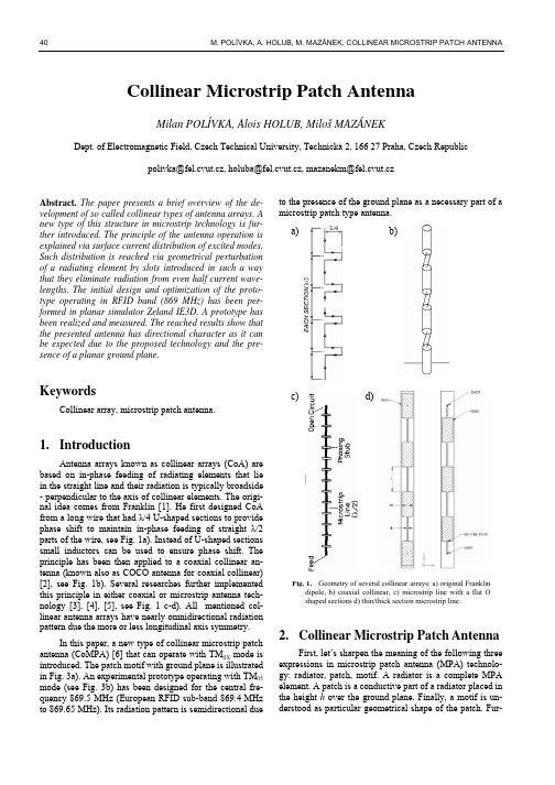
40 M. POLÍVKA, A. HOLUB, M. MAZÁNEK, COLLINEAR MICROSTRIP PATCH ANTENNACollinear Microstrip Patch AntennaMilan POLÍVKA, Alois HOLUB, Miloš MAZÁNEKDept. of Electromagnetic Field, Czech Technical University, Technická 2, 166 27 Praha, Czech Republicpolívka@fel.cvut.cz, holuba@fel.cvut.cz, mazanekm@fel.cvut.czAbstract. The paper presents a brief overview of the de-velopment of so called collinear types of antenna arrays. A new type of this structure in microstrip technology is fur-ther introduced. The principle of the antenna operation is explained via surface current distribution of excited modes. Such distribution is reached via geometrical perturbation of a radiating element by slots introduced in such a way that they eliminate radiation from even half current wave-lengths. The initial design and optimization of the proto-type operating in RFID band (869 MHz) has been per-formed in planar simulator Zeland IE3D. A prototype has been realized and measured. The reached results show that the presented antenna has directional character as it can be expected due to the proposed technology and the pre-sence of a planar ground plane.KeywordsCollinear array, microstrip patch antenna.1.IntroductionAntenna arrays known as collinear arrays (CoA) are based on in-phase feeding of radiating elements that lie in the straight line and their radiation is typically broadside - perpendicular to the axis of collinear elements. The origi-nal idea comes from Franklin [1]. He first designed CoA from a long wire that had λ/4 U-shaped sections to provide phase shift to maintain in-phase feeding of straight λ/2 parts of the wire, see Fig. 1a). Instead of U-shaped sections small inductors can be used to ensure phase shift. The principle has been then applied to a coaxial collinear an-tenna (known also as COCO antenna for coaxial collinear) [2], see Fig. 1b). Several researches further implemented this principle in either coaxial or microstrip antenna tech-nology [3], [4], [5], see Fig. 1 c-d). All mentioned col-linear antenna arrays have nearly omnidirectional radiation pattern due the more or less longitudinal axis symmetry.In this paper, a new type of collinear microstrip patch antenna (CoMPA) [6] that can operate with TM0X mode is introduced. The patch motif with ground plane is illustrated in Fig. 3a). An experimental prototype operating with TM05 mode (see Fig. 3b) has been designed for the central fre-quency 869.5 MHz (European RFID sub-band 869.4 MHz to 869.65 MHz). Its radiation pattern is semidirectional due to the presence of the ground plane as a necessary part of amicrostrip patch type antenna.a)b)c)d)Fig. 1.Geometry of several collinear arrays: a) original Franklin dipole, b) coaxial collinear, c) microstrip line with a flat Oshaped sections d) thin/thick section microstrip line.2.Collinear Microstrip Patch AntennaFirst, let’s sharpen the meaning of the following three expressions in microstrip patch antenna (MPA) technolo-gy: radiator, patch, motif. A radiator is a complete MPA element. A patch is a conductive part of a radiator placed in the height h over the ground plane. Finally, a motif is un-derstood as particular geometrical shape of the patch. Fur-RADIOENGINEERING, VOL. 14, NO. 4, DECEMBER 2005 41 ther, we describe exciting in-phase currents on the planarstructure of CoMPA. The idea is based on the applicationof so called perturbation elements (PE) – geometrical per-turbations of a patch operating with higher order modes.As it is well-known MPA can be designed to operatewith higher order modes. Here TM0X mode (where x de-termines the number of half current wavelengths in theresonant longitudinal dimension of the patch) is used. PEsin the shape of slots are then applied to the structure of thepatch in such a way that they eliminate radiation from evenout-phase half current wavelengths. Specific motif(s) of theperturbed patch thus arise. The simplest example of theusage of the described principle is MPA operating withTM03 mode with one central narrow slot placed in the mid-dle of the patch. The slot of the length approx. λg/2 and thewidth of a fragment of λg causes that second/even currentsflow around the slot (see Fig. 2a). The currents in the vi-cinity of the slot circumference thus cancel their contribu-tions to the radiated fields due to the out-phase orientationon opposite sides. Vector current distribution of MPA ope-rating with TM05 mode with two slots is illustrated in Fig.2b. The same effect around both slots as in case of a motifwith TM03mode can be seen in Fig. 2b.a)b)Fig. 2.Vector surface current distribution on the patch witha) TM03 and b) TM05 modes as modeled in Zeland IE3D withinfinite ground plane.An approximate dimension of the initial model comingfrom the above mentioned idea can be seen in Fig. 3. Suchinitial design has been optimized by means of IE3Dbuild-in procedures with the criteria of impedance match-ing and maximum gain. The dimensions of the optimizedantenna are: the patch 268 x 643 mm and the ground plane298 x680 mm. The height of the patch over the groundplane is 10 mm. The patch was excited by a coaxial feedingplaced on y-axis symmetry in the distance of approx. 0.05λg above the lower slot (see Fig. 3). In IE3D feeding wasmodeled by vertical localized port.The measured reflection coefficient of the realizedprototype with and without 3 mm thick HPS (hardenedpolystyren) radom placed in the height of 40 mm over thepatch is illustrated in Fig. 4.a)b)Fig. PA operating with TM05 mode: a) top view of thelayout with optimized dimensions related to wavelength, b)photograph of the prototype05dielectric cover.42 M. POLÍVKA, A. HOLUB, M. MAZÁNEK, COLLINEAR MICROSTRIP PATCH ANTENNAMeasured radiation patterns are illustrated in Fig. 5. The distance between the middle part of rectangular in-phase source current areas is approx. 0.68 λ0, that’s why the side-lobe level is about –13 dB as in case of 0.5 λ0 spaced uni-form array. The front-back ratio is about 19 dB in E plane and 14 dB in H plane although ground plane dimensions are just only about 0.1 λ0 larger than the patch itself.-40-30-20-100302106024090270120300150330180a)[dB]Eco Ex-40-30-20-100302106024090270120300150330180b)Eco Ex[dB]Fig. 5. Measured radiation patterns of CoMPA operating withTM 05 mode in a) E-plane, b) H-plane.The antenna gain (Tab. 1.) was measured by substitution method at 869 MHz in the antenna anechoic chamber [7] with the help of standard horn antennas. Simulated values of directivity 12.6 dBi and gain 12.4 are a little bit higher than the measured value 11.7 dBi of gain. Of course preci-se gain error estimation could be made but anyway a gain error at least of about +/- 0.5 dBi can be supposed.Simulated directivity [dBi] Simulated gain [dBi] Simulated efficiency [%] Measured gain [dBi] 12.6 12.4 95 11.7Tab. 1. Measured and simulated values of gain, directivity and efficiency.Measured narrower 3 dB beamwidth in E plane (25°) con-firms measurement results (Tab. 2.) that exhibit gain en-hancement compared to gain of standard rectangular mic-rostrip patch operating with TM 01 mode (approx. 6-9 dBi, see for example [8]). Impedance bandwidth is related to the common value of VSWR = 2. The value of BW = 2.8 % is relatively small as in case of microstrip patch antennas ge-nerally. In the particular RFID application the bandwidth is sufficient as just 250 kHz band is required.BW [MHz] BW [%] θ3dB [°] in E plane θ3dB [°] in H plane24 2.8 2562Tab. 2. Measured values of CoMPA with TM 05 mode bandwidthand 3dB beamwidths.3. ConclusionThe novel type of collinear antenna array was propo-sed, designed and realized in microstrip patch antenna technology. The principle of the operation has been expla-ined via surface current distribution on the structure of the antenna and can be described as the slot loaded microstrip patch operating with TM 0x modes. Due to the collinear ar-rangement of in-phase source current areas, the beamwidth in E plane together with directivity can be enhanced by in-creasing the order of operational mode together with enlar-gement of patch resonant dimension. Realization in micro-strip patch antenna technology thus causes that the propo-sed antenna belongs to directive kinds of antennas compa-red to omnidirectional coaxial types of collinear arrays.AcknowledgementThis work has been conducted at the Dept. of Electro-magnetic Field of the Czech Technical University in Pra-gue and supported by the grant of the Czech Grant Agency no. 102/04/P131 Multiband planar antennas with compact-shaped radiators and by the Czech Ministry of Education project Research in the area of the prospective information and navigation technologies MSM 6840770014.References[1] FRANKLIN, C. S. Brit. Patent 242342-1924, 1924.[2] JUDAZS, T. J., BALSLEY, B. B. Improved theoretical and experi-mental models for the coaxial collinear antenna. IEEE Trans. Anten-nas and Propagat . 1989, vol. 37, p.289-296. [3] SOLBACH, K. Microstrip-Franklin Antenna. IEEE Trans. Antennasand Propagat . 1982, vol. 30, no. 4, p. 773-775. [4] ČERNOHORSKÝ, D., NOVÁČEK, Z., Dipole array excited by slotsin its coaxial feeder. Radioengineering. 2001, vol. 10, no. 4, p. 9-16. [5] BANCROFT, R., BATEMAN, B.. An omnidirectional planar micro-strip antenna. IEEE Trans. Antennas and Propagat . 2004, vol. 52, no. 11, p. 3151-3153. [6] POLÍVKA, M., HOLUB, A. CZ Patent Application PUV 2005-396,2005. [7] MAZÁNEK, M., KLEPAL, M., PECHA Č, P., POLÍVKA, M., BAR-TÍK, H. Anechoic and EMC chambers - modelling, design, testing. In Proc. of the Millennium Conference on Antennas and Propaga-tion. Noordwijk, European Space Agency, 2000, vol. 2, p. 156-160. [8] GARG. R., BHARTIA, P. Microstrip Antenna Design Handbook.,Artech House, 2000.。

指南针物理原理知识点The principle of a compass is based on the Earth's magnetic field. 指南针的原理基于地球的磁场。
This magnetic field is generated by the movement of molten iron in the Earth's outer core. 这个磁场是由地球外核内的熔融铁的运动产生的。
As the Earth spins on its axis, this molten iron creates a magnetic field that extends out into space. 随着地球在其轴上旋转,这些熔融的铁形成了一个延伸到太空的磁场。
The compass contains a small, lightweight magnet that is free to align itself with the Earth's magnetic field. 指南针内含有一个小型的轻质磁铁,它能够自由地与地球的磁场保持一致。
When the compass is held level, the magnet within it aligns itself with the Earth's magnetic field and points towards the magnetic north pole. 当指南针保持水平时,其中的磁铁会与地球的磁场保持一致,并指向磁性北极。
This creates a reliable method for determining direction, and has been used by humans for centuries for navigation. 这创造了一种可靠的方向确定方法,几个世纪以来一直被人类用于导航。
Conventional optical components rely on gradual phase shifts accumulated during light propagation to shape light beams. New degrees of freedom are attained by introducing abrupt phase changes over the scale of the wavelength. A two-dimensional array of optical resonators with spatially varying phase response and sub-wavelength separation can imprint such phase discontinuities on propagating light as it traverses the interface between two media. Anomalous reflection and refraction phenomena are observed in this regime in optically thin arrays of metallic antennas on silicon with a linear phase variation along the interface, in excellent agreement with generalized laws derived from Fermat’s principle. Phase discontinuities provide great flexibility in the design of light beams as illustrated by the generation of optical vortices using planar designer metallic interfaces. The shaping of the wavefront of light by optical components such as lenses and prisms, as well as diffractive elements like gratings and holograms, relies on gradual phase changes accumulated along the optical path. This approach is generalized in transformation optics (1, 2) which utilizesmetamaterials to bend light in unusual ways, achieving suchphenomena as negative refraction, subwavelength-focusing,and cloaking (3, 4) and even to explore unusual geometries ofspace-time in the early universe (5). A new degree of freedomof controlling wavefronts can be attained by introducingabrupt phase shifts over the scale of the wavelength along theoptical path, with the propagation of light governed byFermat’s principle. The latter states that the trajectory takenbetween two points A and B by a ray of light is that of leastoptical path, ()B A n r dr ∫r , where ()n r r is the local index of refraction, and readily gives the laws of reflection and refraction between two media. In its most general form,Fermat’s principle can be stated as the principle of stationaryphase (6–8); that is, the derivative of the phase()B A d r ϕ∫r accumulated along the actual light path will be zero with respect to infinitesimal variations of the path. We show that an abrupt phase delay ()s r Φr over the scale of the wavelength can be introduced in the optical path by suitably engineering the interface between two media; ()s r Φr depends on the coordinate s r r along the interface. Then the total phase shift ()B s A r k dr Φ+⋅∫r r r will be stationary for the actual path that light takes; k r is the wavevector of the propagating light. This provides a generalization of the laws of reflection and refraction, which is applicable to a wide range of subwavelength structured interfaces between two media throughout the optical spectrum. Generalized laws of reflection and refraction. The introduction of an abrupt phase delay, denoted as phase discontinuity, at the interface between two media allows us to revisit the laws of reflection and refraction by applying Fermat’s principle. Consider an incident plane wave at an angle θi . Assuming that the two rays are infinitesimally close to the actual light path (Fig. 1), then the phase difference between them is zero ()()()s in s in 0o i i o t t kn d x d kn d x θθ+Φ+Φ−+Φ=⎡⎤⎡⎤⎣⎦⎣⎦ (1) where θt is the angle of refraction, Φ and Φ+d Φ are, respectively, the phase discontinuities at the locations where the two paths cross the interface, dx is the distance between the crossing points, n i and n t are the refractive indices of thetwo media, and k o = 2π/λo , where λo is the vacuumwavelength. If the phase gradient along the interface isdesigned to be constant, the previous equation leads to thegeneralized Snell’s law of refraction Light Propagation with Phase Discontinuities: Generalized Laws of Reflection and RefractionNanfang Yu ,1 Patrice Genevet ,1,2 Mikhail A. Kats ,1 Francesco Aieta ,1,3 Jean-Philippe Tetienne ,1,4 Federico Capasso ,1 Zeno Gaburro 1,51School of Engineering and Applied Sciences, Harvard University, Cambridge, Massachusetts 02138, USA. 2Institute for Quantum Studies and Department of Physics, Texas A&M University, College Station, Texas 77843, USA. 3Dipartimento di Fisica e Ingegneria dei Materiali e del Territorio, Università Politecnica delle Marche, via Brecce Bianche, 60131 Ancona, Italy. 4Laboratoire de Photonique Quantique et Moléculaire, Ecole Normale Supérieure de Cachan and CNRS, 94235 Cachan, France. 5Dipartimento di Fisica, Università degli Studi di Trento, via Sommarive 14, 38100 Trento, Italy.o n S e p t e m b e r 1, 2011w w w .s c i e n c e m a g .o r g D o w n l o a d e d f r o m()()sin sin 2o t t i i d n n dx λθθπΦ−= (2) Equation 2 implies that the refracted ray can have an arbitrary direction, provided that a suitable constant gradient of phase discontinuity along the interface (d Φ/dx ) is introduced. Note that because of the non-zero phase gradient in this modified Snell’s law, the two angles of incidence ±θi lead to different values for the angle of refraction. As a consequence there are two possible critical angles for total internal reflection, provided that n t < n i : arcsin 2to c i i n d n n dx λθπ⎛⎞Φ=±−⎜⎟⎝⎠ (3)Similarly, for the reflected light we have ()()sin sin 2o r i i d n dx λθθπΦ−= (4) where θr is the angle of reflection. Note the nonlinear relationbetween θr and θI , which is markedly different fromconventional specular reflection. Equation 4 predicts that there is always a critical incidence angle arcsin 12o c i d n dx λθπ⎛⎞Φ′=−⎜⎟⎝⎠ (5) above which the reflected beam becomes evanescent. In the above derivation we have assumed that Φ is a continuous function of the position along the interface; thus all the incident energy is transferred into the anomalous reflection and refraction. However because experimentally we use an array of optically thin resonators with sub-wavelength separation to achieve the phase change along the interface, this discreteness implies that there are also regularly reflected and refracted beams, which follow conventional laws of reflection and refraction (i.e., d Φ/dx =0 in Eqs. 2 and 4). The separation between the resonators controls the relative amount of energy in the anomalously reflected and refracted beams. We have also assumed that the amplitudes of the scattered radiation by each resonator are identical, so that the refracted and reflected beams are plane waves. In the next section we will show by simulations, which represent numerical solutions of Maxwell’s equations, how indeed one can achieve the equal-amplitude condition and the constant phase gradient along the interface by suitable design of the resonators. Note that there is a fundamental difference between the anomalous refraction phenomena caused by phase discontinuities and those found in bulk designer metamaterials, which are caused by either negative dielectric permittivity and negative magnetic permeability or anisotropic dielectric permittivity with different signs ofpermittivity tensor components along and transverse to thesurface (3, 4).Phase response of optical antennas. The phase shift between the emitted and the incident radiation of an optical resonator changes appreciably across a resonance. By spatially tailoring the geometry of the resonators in an array and hence their frequency response, one can design the phase shift along the interface and mold the wavefront of the reflected and refracted beams in nearly arbitrary ways. The choice of the resonators is potentially wide-ranging, fromelectromagnetic cavities (9, 10), to nanoparticles clusters (11,12) and plasmonic antennas (13, 14). We concentrated on thelatter, due to their widely tailorable optical properties (15–19)and the ease of fabricating planar antennas of nanoscalethickness. The resonant nature of a rod antenna made of aperfect electric conductor is shown in Fig. 2A (20).Phase shifts covering the 0 to 2π range are needed toprovide full control of the wavefront. To achieve the requiredphase coverage while maintaining large scatteringamplitudes, we utilized the double resonance properties of V-shaped antennas, which consist of two arms of equal length h connected at one end at an angle Δ (Fig. 2B). We define twounit vectors to describe the orientation of a V-antenna: ŝalong the symmetry axis of the antenna and â perpendicular to ŝ (Fig. 2B). V-antennas support “symmetric” and “antisymmetric” modes (middle and right panels of Fig. 2B),which are excited by electric-field components along ŝ and â axes, respectively. In the symmetric mode, the current distribution in each arm approximates that of an individual straight antenna of length h (Fig. 2B middle panel), and therefore the first-order antenna resonance occurs at h ≈ λeff /2, where λeff is the effective wavelength (14). In the antisymmetric mode, the current distribution in each arm approximates that of one half of a straight antenna of length 2h (Fig. 2B right panel), and the condition for the first-order resonance of this mode is 2h ≈ λeff /2.The polarization of the scattered radiation is the same as that of the incident light when the latter is polarized along ŝ or â. For an arbitrary incident polarization, both antenna modes are excited but with substantially different amplitude and phase due to their distinctive resonance conditions. As a result, the scattered light can have a polarization different from that of the incident light. These modal properties of the V-antennas allow one to design the amplitude, phase, and polarization state of the scattered light. We chose the incident polarization to be at 45 degrees with respect to ŝ and â, so that both the symmetric and antisymmetric modes can be excited and the scattered light has a significant component polarized orthogonal to that of the incident light. Experimentally this allows us to use a polarizer to decouple the scattered light from the excitation.o n S e p t e m b e r 1, 2011w w w .s c i e n c e m a g .o r g Do w n l o a d e d f r o mAs a result of the modal properties of the V-antennas and the degrees of freedom in choosing antenna geometry (h and Δ), the cross-polarized scattered light can have a large range of phases and amplitudes for a given wavelength λo; see Figs. 2D and E for analytical calculations of the amplitude and phase response of V-antennas assumed to be made of gold rods. In Fig. 2D the blue and red dashed curves correspond to the resonance peaks of the symmetric and antisymmetric mode, respectively. We chose four antennas detuned from the resonance peaks as indicated by circles in Figs. 2D and E, which provide an incremental phase of π/4 from left to right for the cross-polarized scattered light. By simply taking the mirror structure (Fig. 2C) of an existing V-antenna (Fig. 2B), one creates a new antenna whose cross-polarized emission has an additional π phase shift. This is evident by observing that the currents leading to cross-polarized radiation are π out of phase in Figs. 2B and C. A set of eight antennas were thus created from the initial four antennas as shown in Fig. 2F. Full-wave simulations confirm that the amplitudes of the cross-polarized radiation scattered by the eight antennas are nearly equal with phases in π/4 increments (Fig. 2G).Note that a large phase coverage (~300 degrees) can also be achieved using arrays of straight antennas (fig. S3). However, to obtain the same range of phase shift their scattering amplitudes will be significantly smaller than those of V-antennas (fig. S3). As a consequence of its double resonances, the V-antenna instead allows one to design an array with phase coverage of 2π and equal, yet high, scattering amplitudes for all of the array elements, leading to anomalously refracted and reflected beams of substantially higher intensities.Experiments on anomalous reflection and refraction. We demonstrated experimentally the generalized laws of reflection and refraction using plasmonic interfaces constructed by periodically arranging the eight constituent antennas as explained in the caption of Fig. 2F. The spacing between the antennas should be sub-wavelength to provide efficient scattering and to prevent the occurrence of grating diffraction. However it should not be too small; otherwise the strong near-field coupling between neighboring antennas would perturb the designed scattering amplitudes and phases.A representative sample with the densest packing of antennas, Γ= 11 µm, is shown in Fig. 3A, where Γ is the lateral period of the antenna array. In the schematic of the experimental setup (Fig. 3B), we assume that the cross-polarized scattered light from the antennas on the left-hand side is phase delayed compared to the ones on the right. By substituting into Eq. 2 -2π/Γ for dΦ/dx and the refractive indices of silicon and air (n Si and 1) for n i and n t, we obtain the angle of refraction for the cross-polarized lightθt,٣= arcsin[n Si sin(θi) – λo/Γ] (6) Figure 3C summarizes the experimental results of theordinary and the anomalous refraction for six samples with different Γ at normal incidence. The incident polarization isalong the y-axis in Fig. 3A. The sample with the smallest Γcorresponds to the largest phase gradient and the mostefficient light scattering into the cross polarized beams. We observed that the angles of anomalous refraction agree wellwith theoretical predictions of Eq. 6 (Fig. 3C). The same peak positions were observed for normal incidence withpolarization along the x-axis in Fig. 3A (Fig. 3D). To a good approximation, we expect that the V-antennas were operating independently at the packing density used in experiments (20). The purpose of using a large antenna array (~230 µm ×230 µm) is solely to accommodate the size of the plane-wave-like excitation (beam radius ~100 µm). The periodic antenna arrangement is used here for convenience, but is notnecessary to satisfy the generalized laws of reflection and refraction. It is only necessary that the phase gradient isconstant along the plasmonic interface and that the scattering amplitudes of the antennas are all equal. The phaseincrements between nearest neighbors do not need to be constant, if one relaxes the unnecessary constraint of equal spacing between nearest antennas.Figures 4A and B show the angles of refraction and reflection, respectively, as a function of θi for both thesilicon-air interface (black curves and symbols) and the plasmonic interface (red curves and symbols) (20). In therange of θi = 0-9 degrees, the plasmonic interface exhibits “negative” refraction and reflection for the cross-polarized scattered light (schematics are shown in the lower right insetsof Figs. 4A and B). Note that the critical angle for totalinternal reflection is modified to about -8 and +27 degrees(blue arrows in Fig. 4A) for the plasmonic interface in accordance with Eq. 3 compared to ±17 degrees for thesilicon-air interface; the anomalous reflection does not exist beyond θi = -57 degrees (blue arrow in Fig. 4B).At normal incidence, the ratio of intensity R between the anomalously and ordinarily refracted beams is ~ 0.32 for the sample with Γ = 15 µm (Fig. 3C). R rises for increasingantenna packing densities (Figs. 3C and D) and increasingangles of incidence (up to R≈ 0.97 at θi = 14 degrees (fig.S1B)). Because of the experimental configuration, we are notable to determine the ratio of intensity between the reflected beams (20), but we expect comparable values.Vortex beams created by plasmonic interfaces. To demonstrate the versatility of the concept of interfacial phase discontinuities, we fabricated a plasmonic interface that isable to create a vortex beam (21, 22) upon illumination by normally incident linearly polarized light. A vortex beam hasa helicoidal (or “corkscrew-shaped”) equal-phase wavefront. Specifically, the beam has an azimuthal phase dependenceexp(i lφ) with respect to the beam axis and carries an orbitalonSeptember1,211www.sciencemag.orgDownloadedfromangular momentum of L l=h per photon (23), where the topological charge l is an integer, indicating the number of twists of the wavefront within one wavelength; h is the reduced Planck constant. These peculiar states of light are commonly generated using a spiral phase plate (24) or a computer generated hologram (25) and can be used to rotate particles (26) or to encode information in optical communication systems (27).The plasmonic interface was created by arranging the eight constituent antennas as shown in Figs. 5A and B. The interface introduces a spiral-like phase delay with respect to the planar wavefront of the incident light, thereby creating a vortex beam with l = 1. The vortex beam has an annular intensity distribution in the cross-section, as viewed in a mid-infrared camera (Fig. 5C); the dark region at the center corresponds to a phase singularity (22). The spiral wavefront of the vortex beam can be revealed by interfering the beam with a co-propagating Gaussian beam (25), producing a spiral interference pattern (Fig. 5E). The latter rotates when the path length of the Gaussian beam was changed continuously relative to that of the vortex beam (movie S1). Alternatively, the topological charge l = 1 can be identified by a dislocated interference fringe when the vortex and Gaussian beams interfere with a small angle (25) (Fig. 5G). The annular intensity distribution and the interference patterns were well reproduced in simulations (Figs. D, F, and H) by using the calculated amplitude and phase responses of the V-antennas (Figs. 2D and E).Concluding remarks. Our plasmonic interfaces, consisting of an array of V-antennas, impart abrupt phase shifts in the optical path, thus providing great flexibility in molding of the optical wavefront. This breaks the constraint of standard optical components, which rely on gradual phase accumulation along the optical path to change the wavefront of propagating light. We have derived and experimentally confirmed generalized reflection and refraction laws and studied a series of intriguing anomalous reflection and refraction phenomena that descend from the latter: arbitrary reflection and refraction angles that depend on the phase gradient along the interface, two different critical angles for total internal reflection that depend on the relative direction of the incident light with respect to the phase gradient, critical angle for the reflected light to be evanescent. We have also utilized a plasmonic interface to generate optical vortices that have a helicoidal wavefront and carry orbital angular momentum, thus demonstrating the power of phase discontinuities as a design tool of complex beams. The design strategies presented in this article allow one to tailor in an almost arbitrary way the phase and amplitude of an optical wavefront, which should have major implications for transformation optics and integrated optics. We expect that a variety of novel planar optical components such as phased antenna arrays in the optical domain, planar lenses,polarization converters, perfect absorbers, and spatial phase modulators will emerge from this approach.Antenna arrays in the microwave and millimeter-waveregion have been widely used for the shaping of reflected and transmitted beams in the so-called “reflectarrays” and “transmitarrays” (28–31). There is a connection between thatbody of work and our results in that both use abrupt phase changes associated with antenna resonances. However the generalization of the laws of reflection and refraction wepresent is made possible by the deep-subwavelengththickness of our optical antennas and their subwavelength spacing. It is this metasurface nature of the plasmonicinterface that distinguishes it from reflectarrays and transmitarrays. The last two cannot be treated as an interfacein the effective medium approximation for which one canwrite down the generalized laws, because they typicallyconsist of a double layer structure comprising a planar arrayof antennas, with lateral separation larger than the free-space wavelength, and a ground plane (in the case of reflectarrays)or another array (in the case of transmitarrays), separated by distances ranging from a fraction of to approximately one wavelength. In this case the phase along the plane of the array cannot be treated as a continuous variable. This makes it impossible to derive for example the generalized Snell’s lawin terms of a phase gradient along the interface. This generalized law along with its counterpart for reflectionapplies to the whole optical spectrum for suitable designer interfaces and it can be a guide for the design of new photonic devices.References and Notes1. J. B. Pendry, D. Schurig, D. R. Smith, “Controllingelectromagnetic fields,” Science 312, 1780 (2006).2. U. Leonhardt, “Optical conformal mapping,” Science 312,1777 (2006).3. W. Cai, V. Shalaev, Optical Metamaterials: Fundamentalsand Applications (Springer, 2009)4. N. Engheta, R. W. Ziolkowski, Metamaterials: Physics andEngineering Explorations (Wiley-IEEE Press, 2006).5. I. I Smolyaninov, E. E. Narimanov, Metric signaturetransitions in optical metamaterials. Phys. Rev. Lett.105,067402 (2010).6. S. D. Brorson, H. A. Haus, “Diffraction gratings andgeometrical optics,” J. Opt. Soc. Am. B 5, 247 (1988).7. R. P. Feynman, A. R. Hibbs, Quantum Mechanics andPath Integrals (McGraw-Hill, New York, 1965).8. E. Hecht, Optics (3rd ed.) (Addison Wesley PublishingCompany, 1997).9. H. T. Miyazaki, Y. Kurokawa, “Controlled plasmonnresonance in closed metal/insulator/metal nanocavities,”Appl. Phys. Lett. 89, 211126 (2006).onSeptember1,211www.sciencemag.orgDownloadedfrom10. D. Fattal, J. Li, Z. Peng, M. Fiorentino, R. G. Beausoleil,“Flat dielectric grating reflectors with focusing abilities,”Nature Photon. 4, 466 (2010).11. J. A. Fan et al., “Self-assembled plasmonic nanoparticleclusters,” Science 328, 1135 (2010).12. B. Luk’yanchuk et al., “The Fano resonance in plasmonicnanostructures and metamaterials,” Nature Mater. 9, 707 (2010).13. R. D. Grober, R. J. Schoelkopf, D. E. Prober, “Opticalantenna: Towards a unity efficiency near-field opticalprobe,” Appl. Phys. Lett. 70, 1354 (1997).14. L. Novotny, N. van Hulst, “Antennas for light,” NaturePhoton. 5, 83 (2011).15. Q. Xu et al., “Fabrication of large-area patternednanostructures for optical applications by nanoskiving,”Nano Lett. 7, 2800 (2007).16. M. Sukharev, J. Sung, K. G. Spears, T. Seideman,“Optical properties of metal nanoparticles with no center of inversion symmetry: Observation of volume plasmons,”Phys. Rev. B 76, 184302 (2007).17. P. Biagioni, J. S. Huang, L. Duò, M. Finazzi, B. Hecht,“Cross resonant optical antenna,” Phys. Rev. Lett. 102,256801 (2009).18. S. Liu et al., “Double-grating-structured light microscopyusing plasmonic nanoparticle arrays,” Opt. Lett. 34, 1255 (2009).19. J. Ginn, D. Shelton, P. Krenz, B. Lail, G. Boreman,“Polarized infrared emission using frequency selectivesurfaces,” Opt. Express 18, 4557 (2010).20. Materials and methods are available as supportingmaterial on Science Online.21. J. F. Nye, M. V. Berry, “Dislocations in wave trains,”Proc. R. Soc. Lond. A. 336, 165 (1974).22. M. Padgett, J. Courtial, L. Allen, “Ligh’'s orbital angularmomentum,” Phys. Today 57, 35 (2004).23. L. Allen, M. W. Beijersbergen, R. J. C. Spreeuw, J. P.Woerdman, “Orbital angular momentum of light and the transformation of Laguerre-Gaussian laser modes,” Phys.Rev. A, 45, 8185 (1992).24. M. W. Beijersbergen, R. P. C. Coerwinkel, M. Kristensen,J. P. Woerdman, “Helical-wavefront laser beams produced with a spiral phaseplate,” Opt. Commun. 112, 321 (1994).25. N. R. Heckenberg, R. McDuff, C. P. Smith, A. G. White,“Generation of optical phase singularities by computer-generated holograms,” Opt. Lett. 17, 221 (1992).26. H. He, M. E. J. Friese, N. R. Heckenberg, H. Rubinsztein-Dunlop, “Direct observation of transfer of angularmomentum to absorptive particles from a laser beam witha phase singularity,” Phys. Rev. Lett. 75, 826 (1995).27. G. Gibson et al, “Free-space information transfer usinglight beams carrying orbital angular momentum,” Opt.Express 12, 5448 (2004). 28. D. M. Pozar, S. D. Targonski, H. D. Syrigos, “Design ofmillimeter wave microstrip reflectarrays,” IEEE Trans.Antennas Propag. 45, 287 (1997).29. J. A. Encinar, “Design of two-layer printed reflectarraysusing patches of variable size,” IEEE Trans. AntennasPropag. 49, 1403 (2001).30. C. G. M. Ryan et al., “A wideband transmitarray usingdual-resonant double square rings,” IEEE Trans. AntennasPropag. 58, 1486 (2010).31. P. Padilla, A. Muñoz-Acevedo, M. Sierra-Castañer, M.Sierra-Pérez, “Electronically reconfigurable transmitarrayat Ku band for microwave applications,” IEEE Trans.Antennas Propag. 58, 2571 (2010).32. H. R. Philipp, “The infrared optical properties of SiO2 andSiO2 layers on silicon,” J. Appl. Phys. 50, 1053 (1979).33. R. W. P. King, The Theory of Linear Antennas (HarvardUniversity Press, 1956).34. J. D. Jackson, Classical Electrodynamics (3rd edition)(John Wiley & Sons, Inc. 1999) pp. 665.35. E. D. Palik, Handbook of Optical Constants of Solids(Academic Press, 1998).36. I. Puscasu, D. Spencer, G. D. Boreman, “Refractive-indexand element-spacing effects on the spectral behavior ofinfrared frequency-selective surfaces,” Appl. Opt. 39,1570 (2000).37. G. W. Hanson, “On the applicability of the surfaceimpedance integral equation for optical and near infraredcopper dipole antennas,” IEEE Trans. Antennas Propag.54, 3677 (2006).38. C. R. Brewitt-Taylor, D. J. Gunton, H. D. Rees, “Planarantennas on a dielectric surface,” Electron. Lett. 17, 729(1981).39. D. B. Rutledge, M. S. Muha, “Imaging antenna arrays,”IEEE Trans. Antennas Propag. 30, 535 (1982). Acknowledgements: The authors acknowledge helpful discussion with J. Lin, R. Blanchard, and A. Belyanin. Theauthors acknowledge support from the National ScienceFoundation, Harvard Nanoscale Science and EngineeringCenter (NSEC) under contract NSF/PHY 06-46094, andthe Center for Nanoscale Systems (CNS) at HarvardUniversity. Z. G. acknowledges funding from theEuropean Communities Seventh Framework Programme(FP7/2007-2013) under grant agreement PIOF-GA-2009-235860. M.A.K. is supported by the National ScienceFoundation through a Graduate Research Fellowship.Harvard CNS is a member of the NationalNanotechnology Infrastructure Network (NNIN). TheLumerical FDTD simulations in this work were run on theOdyssey cluster supported by the Harvard Faculty of Artsand Sciences (FAS) Sciences Division ResearchComputing Group.onSeptember1,211www.sciencemag.orgDownloadedfrom。
指南针英文介绍讲解学习(第1页)一、引言:认识指南针(Introduction to Compass)指南针,一种古老的导航工具,自古以来便为人类探索未知世界提供了方向。
在英文中,指南针被称为“Compass”,今天我们将一起学习关于指南针的英文介绍。
二、指南针的历史(History of Compass)1. 起源(Origin)指南针最早起源于中国,大约在公元前4世纪,我国先民们发现了磁铁的性质,并制成了最早的指南针。
当时的指南针主要用于风水和占卜。
2. 传播与发展(Spread and Development)随着时间的推移,指南针逐渐传入阿拉伯地区,后来又传到了欧洲。
在15世纪,指南针成为航海家们探险的重要工具,为地理大发现奠定了基础。
三、指南针的工作原理(Working Principle of Compass)1. 地球磁场(Earth's Magnetic Field)指南针之所以能指示方向,是因为地球本身就是一个巨大的磁体。
地球的磁场分为南极和北极,指南针的磁针会指向地球的磁北极。
2. 磁针指向(Magnetic Needle Direction)指南针的磁针一端指向地球的磁北极,另一端指向磁南极。
在英文中,指向磁北极的一端被称为“North Pole”,指向磁南极的一端被称为“South Pole”。
四、指南针的种类(Types of Compass)1. 干扰式指南针(Dry Compass)干扰式指南针是最常见的指南针类型,其特点是磁针悬浮在液体(如油或酒精)中,以减少摩擦。
2. 指南针罗盘(Compass Card)指南针罗盘通常用于航海,其特点是磁针固定在一个可旋转的圆盘上,圆盘上刻有方位刻度。
指南针英文介绍讲解学习(第2页)五、指南针的应用(Applications of Compass)1. 航海导航(Maritime Navigation)在航海领域,指南针是最基本的导航工具之一。