先进的PFC PWM组合控制UCC28510
- 格式:doc
- 大小:202.50 KB
- 文档页数:9
IMPORTANT NOTICETexas Instruments Incorporated and its subsidiaries(TI)reserve the right to make corrections,modifications,enhancements,improvements, and other changes to its products and services at any time and to discontinue any product or service without notice.Customers should obtain the latest relevant information before placing orders and should verify that such information is current and complete.All products are sold subject to TI’s terms and conditions of sale supplied at the time of order acknowledgment.TI warrants performance of its hardware products to the specifications applicable at the time of sale in accordance with TI’s standard warranty.Testing and other quality control techniques are used to the extent TI deems necessary to support this warranty.Except where mandated by government requirements,testing of all parameters of each product is not necessarily performed.TI assumes no liability for applications assistance or customer product design.Customers are responsible for their products and applications using TI components.To minimize the risks associated with customer products and applications,customers should provide adequate design and operating safeguards.TI does not warrant or represent that any license,either express or implied,is granted under any TI patent right,copyright,mask work right, or other TI intellectual property right relating to any combination,machine,or process in which TI products or services are rmation published by TI regarding third-party products or services does not constitute a license from TI to use such products or services or a warranty or endorsement e of such information may require a license from a third party under the patents or other intellectual property of the third party,or a license from TI under the patents or other intellectual property of TI.Reproduction of TI information in TI data books or data sheets is permissible only if reproduction is without alteration and is accompanied by all associated warranties,conditions,limitations,and notices.Reproduction of this information with alteration is an unfair and deceptive business practice.TI is not responsible or liable for such altered rmation of third parties may be subject to additional restrictions.Resale of TI products or services with statements different from or beyond the parameters stated by TI for that product or service voids all express and any implied warranties for the associated TI product or service and is an unfair and deceptive business practice.TI is not responsible or liable for any such statements.TI products are not authorized for use in safety-critical applications(such as life support)where a failure of the TI product would reasonably be expected to cause severe personal injury or death,unless officers of the parties have executed an agreement specifically governing such use.Buyers represent that they have all necessary expertise in the safety and regulatory ramifications of their applications,and acknowledge and agree that they are solely responsible for all legal,regulatory and safety-related requirements concerning their products and any use of TI products in such safety-critical applications,notwithstanding any applications-related information or support that may be provided by TI.Further,Buyers must fully indemnify TI and its representatives against any damages arising out of the use of TI products in such safety-critical applications.TI products are neither designed nor intended for use in military/aerospace applications or environments unless the TI products are specifically designated by TI as military-grade or"enhanced plastic."Only products designated by TI as military-grade meet military specifications.Buyers acknowledge and agree that any such use of TI products which TI has not designated as military-grade is solely at the Buyer's risk,and that they are solely responsible for compliance with all legal and regulatory requirements in connection with such use. TI products are neither designed nor intended for use in automotive applications or environments unless the specific TI products are designated by TI as compliant with ISO/TS16949requirements.Buyers acknowledge and agree that,if they use any non-designated products in automotive applications,TI will not be responsible for any failure to meet such requirements.Following are URLs where you can obtain information on other Texas Instruments products and application solutions:Products ApplicationsAudio /audio Automotive and Transportation /automotiveAmplifiers Communications and Telecom /communicationsData Converters Computers and Peripherals /computersDLP®Products Consumer Electronics /consumer-appsDSP Energy and Lighting /energyClocks and Timers /clocks Industrial /industrialInterface Medical /medicalLogic Security /securityPower Mgmt Space,Avionics and Defense /space-avionics-defense Microcontrollers Video and Imaging /videoRFID OMAP Mobile Processors /omapWireless Connectivity /wirelessconnectivityTI E2E Community Home Page Mailing Address:Texas Instruments,Post Office Box655303,Dallas,Texas75265Copyright©2012,Texas Instruments Incorporated。
i CBSTi CBST= i D1− i Q2Figure 8. Timing Waveforms for Synchronization SchemePACKAGING INFORMATIONOrderable Device Status(1)PackageType PackageDrawingPins PackageQtyEco Plan(2)Lead/Ball Finish MSL Peak Temp(3)UCC28500DW ACTIVE SOIC DW2025Green(RoHS&no Sb/Br)CU NIPDAU Level-2-260C-1YEARUCC28500DWG4ACTIVE SOIC DW2025Green(RoHS&no Sb/Br)CU NIPDAU Level-2-260C-1YEARUCC28500N ACTIVE PDIP N2020Green(RoHS&no Sb/Br)CU NIPDAU N/A for Pkg TypeUCC28500NG4ACTIVE PDIP N2020Green(RoHS&no Sb/Br)CU NIPDAU N/A for Pkg TypeUCC28501DW ACTIVE SOIC DW2025Green(RoHS&no Sb/Br)CU NIPDAU Level-2-260C-1YEARUCC28501DWG4ACTIVE SOIC DW2025Green(RoHS&no Sb/Br)CU NIPDAU Level-2-260C-1YEARUCC28501DWTR ACTIVE SOIC DW202000Green(RoHS&no Sb/Br)CU NIPDAU Level-2-260C-1YEARUCC28501DWTRG4ACTIVE SOIC DW202000Green(RoHS&no Sb/Br)CU NIPDAU Level-2-260C-1YEARUCC28501N ACTIVE PDIP N2020Green(RoHS&no Sb/Br)CU NIPDAU N/A for Pkg TypeUCC28501NG4ACTIVE PDIP N2020Green(RoHS&no Sb/Br)CU NIPDAU N/A for Pkg TypeUCC28502DW ACTIVE SOIC DW2025Green(RoHS&no Sb/Br)CU NIPDAU Level-2-260C-1YEARUCC28502DWG4ACTIVE SOIC DW2025Green(RoHS&no Sb/Br)CU NIPDAU Level-2-260C-1YEARUCC28503DW ACTIVE SOIC DW2025Green(RoHS&no Sb/Br)CU NIPDAU Level-2-260C-1YEARUCC28503DWG4ACTIVE SOIC DW2025Green(RoHS&no Sb/Br)CU NIPDAU Level-2-260C-1YEARUCC38500DW ACTIVE SOIC DW2025Green(RoHS&no Sb/Br)CU NIPDAU Level-2-260C-1YEARUCC38500DWG4ACTIVE SOIC DW2025Green(RoHS&no Sb/Br)CU NIPDAU Level-2-260C-1YEARUCC38500N ACTIVE PDIP N2020Green(RoHS&no Sb/Br)CU NIPDAU N/A for Pkg TypeUCC38500NG4ACTIVE PDIP N2020Green(RoHS&no Sb/Br)CU NIPDAU N/A for Pkg TypeUCC38501DW ACTIVE SOIC DW2025Green(RoHS&no Sb/Br)CU NIPDAU Level-2-260C-1YEARUCC38501DWG4ACTIVE SOIC DW2025Green(RoHS&no Sb/Br)CU NIPDAU Level-2-260C-1YEARUCC38501DWTR ACTIVE SOIC DW202000Green(RoHS&no Sb/Br)CU NIPDAU Level-2-260C-1YEARUCC38501DWTRG4ACTIVE SOIC DW202000Green(RoHS&no Sb/Br)CU NIPDAU Level-2-260C-1YEARUCC38501N ACTIVE PDIP N2020Green(RoHS&no Sb/Br)CU NIPDAU N/A for Pkg TypeUCC38501NG4ACTIVE PDIP N2020Green(RoHS&no Sb/Br)CU NIPDAU N/A for Pkg TypeUCC38502DW ACTIVE SOIC DW2025Green(RoHS&no Sb/Br)CU NIPDAU Level-2-260C-1YEAROrderable Device Status(1)PackageType PackageDrawingPins PackageQtyEco Plan(2)Lead/Ball Finish MSL Peak Temp(3)UCC38502DWG4ACTIVE SOIC DW2025Green(RoHS&no Sb/Br)CU NIPDAU Level-2-260C-1YEARUCC38502DWTR ACTIVE SOIC DW202000Green(RoHS&no Sb/Br)CU NIPDAU Level-2-260C-1YEARUCC38502DWTRG4ACTIVE SOIC DW202000Green(RoHS&no Sb/Br)CU NIPDAU Level-2-260C-1YEARUCC38502N ACTIVE PDIP N2020Green(RoHS&no Sb/Br)CU NIPDAU N/A for Pkg TypeUCC38502NG4ACTIVE PDIP N2020Green(RoHS&no Sb/Br)CU NIPDAU N/A for Pkg TypeUCC38503DW ACTIVE SOIC DW2025Green(RoHS&no Sb/Br)CU NIPDAU Level-2-260C-1YEARUCC38503DWG4ACTIVE SOIC DW2025Green(RoHS&no Sb/Br)CU NIPDAU Level-2-260C-1YEARUCC38503DWTR ACTIVE SOIC DW202000Green(RoHS&no Sb/Br)CU NIPDAU Level-2-260C-1YEARUCC38503DWTRG4ACTIVE SOIC DW202000Green(RoHS&no Sb/Br)CU NIPDAU Level-2-260C-1YEARUCC38503N ACTIVE PDIP N2020Green(RoHS&no Sb/Br)CU NIPDAU N/A for Pkg TypeUCC38503NG4ACTIVE PDIP N2020Green(RoHS&no Sb/Br)CU NIPDAU N/A for Pkg Type(1)The marketing status values are defined as follows:ACTIVE:Product device recommended for new designs.LIFEBUY:TI has announced that the device will be discontinued,and a lifetime-buy period is in effect.NRND:Not recommended for new designs.Device is in production to support existing customers,but TI does not recommend using this part in a new design.PREVIEW:Device has been announced but is not in production.Samples may or may not be available.OBSOLETE:TI has discontinued the production of the device.(2)Eco Plan-The planned eco-friendly classification:Pb-Free(RoHS),Pb-Free(RoHS Exempt),or Green(RoHS&no Sb/Br)-please check /productcontent for the latest availability information and additional product content details.TBD:The Pb-Free/Green conversion plan has not been defined.Pb-Free(RoHS):TI's terms"Lead-Free"or"Pb-Free"mean semiconductor products that are compatible with the current RoHS requirements for all6substances,including the requirement that lead not exceed0.1%by weight in homogeneous materials.Where designed to be soldered at high temperatures,TI Pb-Free products are suitable for use in specified lead-free processes.Pb-Free(RoHS Exempt):This component has a RoHS exemption for either1)lead-based flip-chip solder bumps used between the die and package,or2)lead-based die adhesive used between the die and leadframe.The component is otherwise considered Pb-Free(RoHS compatible)as defined above.Green(RoHS&no Sb/Br):TI defines"Green"to mean Pb-Free(RoHS compatible),and free of Bromine(Br)and Antimony(Sb)based flame retardants(Br or Sb do not exceed0.1%by weight in homogeneous material)(3)MSL,Peak Temp.--The Moisture Sensitivity Level rating according to the JEDEC industry standard classifications,and peak solder temperature.Important Information and Disclaimer:The information provided on this page represents TI's knowledge and belief as of the date that it is provided.TI bases its knowledge and belief on information provided by third parties,and makes no representation or warranty as to the accuracy of such information.Efforts are underway to better integrate information from third parties.TI has taken and continues to take reasonable steps to provide representative and accurate information but may not have conducted destructive testing or chemical analysis on incoming materials and chemicals.TI and TI suppliers consider certain information to be proprietary,and thus CAS numbers and other limited information may not be available for release.In no event shall TI's liability arising out of such information exceed the total purchase price of the TI part(s)at issue in this document sold by TI to Customer on an annual basis.TAPE AND REEL INFORMATION*All dimensions are nominalDevicePackage Type Package Drawing Pins SPQReel Diameter (mm)Reel Width W1(mm)A0(mm)B0(mm)K0(mm)P1(mm)W (mm)Pin1Quadrant UCC28501DWTR SOIC DW 202000330.024.410.813.0 2.712.024.0Q1UCC38501DWTR SOIC DW 202000330.024.410.813.0 2.712.024.0Q1UCC38502DWTR SOIC DW 202000330.024.410.813.0 2.712.024.0Q1UCC38503DWTRSOICDW202000330.024.410.813.02.712.024.0Q1*All dimensions are nominalDevice Package Type Package Drawing Pins SPQ Length(mm)Width(mm)Height(mm) UCC28501DWTR SOIC DW202000346.0346.041.0 UCC38501DWTR SOIC DW202000346.0346.041.0 UCC38502DWTR SOIC DW202000346.0346.041.0 UCC38503DWTR SOIC DW202000346.0346.041.0IMPORTANT NOTICETexas Instruments Incorporated and its subsidiaries(TI)reserve the right to make corrections,modifications,enhancements,improvements, and other changes to its products and services at any time and to discontinue any product or service without notice.Customers should obtain the latest relevant information before placing orders and should verify that such information is current and complete.All products are sold subject to TI’s terms and conditions of sale supplied at the time of order acknowledgment.TI warrants performance of its hardware products to the specifications applicable at the time of sale in accordance with TI’s standard warranty.Testing and other quality control techniques are used to the extent TI deems necessary to support this warranty.Except where mandated by government requirements,testing of all parameters of each product is not necessarily performed.TI assumes no liability for applications assistance or customer product design.Customers are responsible for their products and applications using TI components.To minimize the risks associated with customer products and applications,customers should provide adequate design and operating safeguards.TI does not warrant or represent that any license,either express or implied,is granted under any TI patent right,copyright,mask work right, or other TI intellectual property right relating to any combination,machine,or process in which TI products or services are rmation published by TI regarding third-party products or services does not constitute a license from TI to use such products or services or a warranty or endorsement e of such information may require a license from a third party under the patents or other intellectual property of the third party,or a license from TI under the patents or other intellectual property of TI.Reproduction of TI information in TI data books or data sheets is permissible only if reproduction is without alteration and is accompanied by all associated warranties,conditions,limitations,and notices.Reproduction of this information with alteration is an unfair and deceptive business practice.TI is not responsible or liable for such altered rmation of third parties may be subject to additional restrictions.Resale of TI products or services with statements different from or beyond the parameters stated by TI for that product or service voids all express and any implied warranties for the associated TI product or service and is an unfair and deceptive business practice.TI is not responsible or liable for any such statements.TI products are not authorized for use in safety-critical applications(such as life support)where a failure of the TI product would reasonably be expected to cause severe personal injury or death,unless officers of the parties have executed an agreement specifically governing such use.Buyers represent that they have all necessary expertise in the safety and regulatory ramifications of their applications,and acknowledge and agree that they are solely responsible for all legal,regulatory and safety-related requirements concerning their products and any use of TI products in such safety-critical applications,notwithstanding any applications-related information or support that may be provided by TI.Further,Buyers must fully indemnify TI and its representatives against any damages arising out of the use of TI products in such safety-critical applications.TI products are neither designed nor intended for use in military/aerospace applications or environments unless the TI products are specifically designated by TI as military-grade or"enhanced plastic."Only products designated by TI as military-grade meet military specifications.Buyers acknowledge and agree that any such use of TI products which TI has not designated as military-grade is solely at the Buyer's risk,and that they are solely responsible for compliance with all legal and regulatory requirements in connection with such use. TI products are neither designed nor intended for use in automotive applications or environments unless the specific TI products are designated by TI as compliant with ISO/TS16949requirements.Buyers acknowledge and agree that,if they use any non-designated products in automotive applications,TI will not be responsible for any failure to meet such requirements.Following are URLs where you can obtain information on other Texas Instruments products and application solutions:Products ApplicationsAmplifiers AudioData Converters AutomotiveDSP BroadbandClocks and Timers Digital ControlInterface MedicalLogic MilitaryPower Mgmt Optical NetworkingMicrocontrollers SecurityRFID TelephonyRF/IF and ZigBee®Solutions Video&ImagingWirelessMailing Address:Texas Instruments,Post Office Box655303,Dallas,Texas75265Copyright©2008,Texas Instruments Incorporated。

提高电源转换效率的交错式PFC控制技术及应用多年以来,多种创新型功率因数校正(PFC)技术不断问世。
采纳升压拓扑结构的有源功率因数校正就是首批创新技术中的一种。
因为不再需要大体积的无源PFC解决计划,所以有源功率因数校正技术提高了功率密度。
另一个创新技术为转移模式PFC,该技术消退了PFC预调整器的升压中的反向复原,不但降低了转换器的开关损耗,而且还提高了系统效率。
用来增强功率密度并提高系统效率的PFC下一个创新技术为交叉式PFC预调整器。
电源设计工程师设计交叉式PFC转换器已有数年,但因缺少合适的控制器,所以对电源控制的设计必需十分谨慎。
为使交叉式PFC设计变得更轻松,(TI)开发出两款交叉式PFC控制器:一款为针对平均电流模式预调整器的控制器(UCC28070),另一款为针对交叉式转移模式PFC预调整器的控制器(UCC28060)。
本文将研究如何利用交叉式PFC及其控制技术来增强功率密度、提高系统效率并降低系统成本。
交叉式PFC升压预调整器(图1)仅由两个PFC升压转换器组成,这两个升压转换器的工作相位相差180°,可降低由电流(IL1和IL2)引起的输入电流(IIN)。
因为电感高频纹波电流为反相,所以二者互相抵销,从而降低由升压电感电流引起的输入纹波电流。
电感纹波电流的消退允许电源设计工程师在削减由升压电感引起的输入纹波的同时并联升压PFC预调整器,这可以降低总的电感升压幅度和/或缩小EMI尺寸。
此外,与单级拓扑结构相比,交叉式PFC预调整器的高频输出的均方根(RMS)电流(ICOUT)不到前者的50%。
高频升压电容的RMS电流的削减最多可以使升压电容数量下降25%。
请不要将升压电容数量与设计时所需的电容数量相混淆,转换器所需的电容数量普通由保持时光打算。
图1:交叉式PFC升压预调整器仅由两个PFC升压转换器。
第1页共4页。

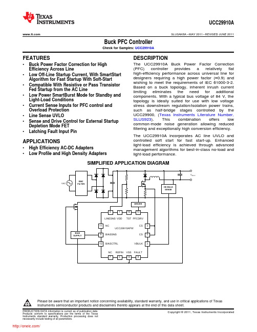
UCC29910A SLUSAK8A–MAY2011–REVISED JUNE2011Buck PFC ControllerCheck for Samples:UCC29910AFEATURES DESCRIPTIONThe UCC29910A Buck Power Factor Correction •Buck Power Factor Correction for High(PFC)controller provides a relatively flat Efficiency Across Linehigh-efficiency performance across universal line for •Low Off-Line Startup Current,With SmartStartdesigners requiring a high power factor(>0.9)and Algorithm for Fast Startup With Soft-Startwishing to meet the requirements of IEC61000-3-2.•Compatible With Resistive or Pass Transistor Based on a buck topology,inherent inrush current Fed Startup from the AC Line limiting eliminates the need for additional •Low Power SmartBurst Mode for Standby and components.With a typical bus voltage of84V,the Light-Load Conditions topology is ideally suited for use with low voltagestress downstream regulation/isolation power trains,•Current Sense Inputs for PFC control andsuch as half-bridge stages controlled by the Overload ProtectionUCC29900,(Texas Instruments Literature Number,•Line Sense UVLOSLUS923).This combination offers low •Sense and Drive Control for External Startupcommon-mode noise generation allowing reduced Depletion Mode FETfiltering and exceptionally high conversion efficiency.•Latching Fault Input PinThe UCC29910A incorporates AC line UVLO andcontrolled soft start for fast start-up.Enhanced APPLICATIONSlight-load efficiency is achieved through advanced •High Efficiency AC-DC Adapters management algorithms for best-in-class no-load and •Low Profile and High Density Adapters light-load performance.SIMPLIFIED APPLICATION DIAGRAMPlease be aware that an important notice concerning availability,standard warranty,and use in critical applications of TexasInstruments semiconductor products and disclaimers thereto appears at the end of this data sheet.PRODUCTION DATA information is current as of publication date.Copyright©2011,Texas Instruments Incorporated Products conform to specifications per the terms of the TexasInstruments standard warranty.Production processing does notnecessarily include testing of all parameters.UCC29910ASLUSAK8A–MAY2011–REVISED This integrated circuit can be damaged by ESD.Texas Instruments recommends that all integrated circuits be handled with appropriate precautions.Failure to observe proper handling and installation procedures can cause damage.ESD damage can range from subtle performance degradation to complete device failure.Precision integrated circuits may be more susceptible to damage because very small parametric changes could cause the device not to meet its published specifications.ORDERING INFORMATIONPART NUMBER PACKAGE PACKINGUCC29910APW Plastic,14-Pin TSSOP(PW)90-Pc.TubeUCC29910APWR Plastic,14-Pin TSSOP(PW)2000-Pc.Tape and ReelABSOLUTE MAXIMUM RATINGSover operating free-air temperature range(unless otherwise noted)(1)(2)(3)VALUE UNIT4.1V DD Supply Voltage-0.3V Voltage:All pins−0.3to VDD+0.3T A Operating free air temperature,(4)−40to105T J Operational junction temperature,(4)°C T STG Storage temperature(4)−40to105Lead temperature(10seconds)260(1)These are stress limits.Stress beyond these limits may cause permanent damage to the device.Functional operation of the device atthese or any conditions beyond those indicated under RECOMMENDED OPERATING CONDITIONS is not implied.Exposure to absolute maximum rated conditions for extended periods of time may affect device reliability.(2)All voltages are with respect to VSS.(3)All currents are positive into the terminal,negative out of the terminal.(4)Higher temperature may be applied during board soldering process according to the current JEDEC J-STD-020specification with peakreflow temperatures not higher than classified on the device label on the shipping boxes or reels.THERMAL INFORMATIONTHERMAL METRIC(1)UNITSPINSθJA Junction-to-ambient thermal resistance(2)θJCtop Junction-to-case(top)thermal resistance(3)θJB Junction-to-board thermal resistance(4)°C/WψJT Junction-to-top characterization parameter(5)ψJB Junction-to-board characterization parameter(6)θJCbot Junction-to-case(bottom)thermal resistance(7)(1)For more information about traditional and new thermal metrics,see the IC Package Thermal Metrics application report,SPRA953.(2)The junction-to-ambient thermal resistance under natural convection is obtained in a simulation on a JEDEC-standard,high-K board,asspecified in JESD51-7,in an environment described in JESD51-2a.(3)The junction-to-case(top)thermal resistance is obtained by simulating a cold plate test on the package top.No specificJEDEC-standard test exists,but a close description can be found in the ANSI SEMI standard G30-88.(4)The junction-to-board thermal resistance is obtained by simulating in an environment with a ring cold plate fixture to control the PCBtemperature,as described in JESD51-8.(5)The junction-to-top characterization parameter,ψJT,estimates the junction temperature of a device in a real system and is extractedfrom the simulation data for obtainingθJA,using a procedure described in JESD51-2a(sections6and7).(6)The junction-to-board characterization parameter,ψJB,estimates the junction temperature of a device in a real system and is extractedfrom the simulation data for obtainingθJA,using a procedure described in JESD51-2a(sections6and7).(7)The junction-to-case(bottom)thermal resistance is obtained by simulating a cold plate test on the exposed(power)pad.No specificJEDEC standard test exists,but a close description can be found in the ANSI SEMI standard G30-88.2Submit Documentation Feedback Copyright©2011,Texas Instruments IncorporatedProduct Folder Link(s):UCC29910AUCC29910A SLUSAK8A–MAY2011–REVISED JUNE2011RECOMMENDED OPERATING CONDITIONSover operating free-air temperature range,all the voltages refer to the VSS pin(unless otherwise noted)MIN NOM MAX UNITT A Operating free air temperature−40105°C VDD Input Voltage 3.0 3.6V All Inputs0VDDELECTRICAL CHARACTERISTICSover operating free-air temperature range(unless otherwise noted)PARAMETER TEST CONDITIONS MIN TYP MAX UNIT Supply CurrentI VDD Operating current V DD=3.3V58mA Voltage Monitoring(1)V NM VBULK nominal Normal mode(2)PFCDRV=100kHz 1.042 1.048 1.054VV BH VLINESNS start-up VB(min)<VBIASSNS<V B(max)258264270V BL VLINESNS brownout Normal mode(2)243249255mVRMS V LM VLINESNS max Normal mode(2)925931937V B(maxVBIASSNS max VLINESNS>V BH907913919)mVV B(min)VBIASSNS min VLINESNS>V BH451457463FAULT Inputt f Latch Time(3)Normal mode(2),FAULT pin goes<0.8V100µsPositive going input thresholdV IT+ 1.45 2.5 voltageNegative going input thresholdV IT-0.8 1.85V voltageInput voltage hysteresis VIT+-V HYS0.31 VIT-PFCDRV sectionf SW Switching frequency Normal mode(2)94100106kHzAt PFCDRV pin,normal mode(2),VLINESNS=V BH,D MAX Max duty cycle89%90%91%VBULK=1.025VVDD-I O=-1.5mA VDD0.25VHigh level output voltage atV OHPFCDRV pin VDD-I O=-6mA VDD V0.6VI O=1.5mA00.25Low Level Output Voltage atV OLPFCDRV pin I=6mA00.6OBIASCTRL OutputLow level output voltage at Start-up mode(4),VBIASSNS increasing and<V BC00.25 BIASCTRL pin V B(max),I O=1.5mAV High level output voltage at Start-up mode(4),VBIASSNS decreasing and>VDD-VDD BIASCTRL pin V B(min),I O=-1.5mA0.25V(1)VBULK,VLINESNS and VBIASSNS voltage thresholds are based on VREFIN=1.500V.These will change proportionally as VREFINchanges.Input bias current at these pins is±50nA max.(2)Normal mode entered when VDD present,V REFIN=1.500V,VLINESNS increased from0to V BH<VLINESNS<V LM,VBIASSNSincreased from0to V B(max)<VBIASSNS<1.025V then reduced to V B(min)<VBIASSNS<V B(max),V CS=150mV,VBULK increased to V NM then reduced to1.025V.There is a600-ms timeout on this process.(3)FAULT inputs shorter than t f cause a non-latched shutdown.FAULT inputs longer than t f cause a latched shutdown.(4)Start-up mode entered when VDD present,VLINESNS increased from0to V BH<VLINESNS<V LM,VBIASSNS increased from0toV B(max)<VBIASSNS<1.025V then reduced to V B(min)<VBIASSNS<V B(max),VBULK=0V.There is a600ms timeout on this process.Copyright©2011,Texas Instruments Incorporated Submit Documentation Feedback3Product Folder Link(s):UCC29910AVDD VSS VBULKCS LINESNSCS REFIN NCFAULTBIASSNS TST NC BIASCTRL PFCDRV UCC29910ASLUSAK8A –MAY 2011–REVISED JUNE 2011DEVICE INFORMATIONTERMINAL FUNCTIONSTERMINALI/O DESCRIPTIONNAME NO.Provides power to the device;should be decoupled with ceramic capacitor (1µF),connected VDD 1-directly across pins 1-14.VBULK 2I Voltage sensing of the bulk capacitor.CS 3I Current sense input for PFC stage.LINESNS 4I Rectified AC line sense input.CS 5I Current sense input for PFC stage.REFIN 6I Reference input for internal comparators/error amplifier.NC 7-NC,this pin is not used,and should be left open.FAULT 8I Fault input for over-voltage or over-load protection.BIASSNS 9I Sense input for the bias rail for startup control.TST 10I This pin should be connected directly to VDD.NC 11-No connection should be made to this pin.BIASCTRL 12O Control output for the external startup FET for startup control.PFCDRV 13O Drive for PFC FET.VSS14-Ground for internal circuitry.4Submit Documentation FeedbackCopyright ©2011,Texas Instruments IncorporatedProduct Folder Link(s):UCC29910AUCC29910A SLUSAK8A–MAY2011–REVISED JUNE2011Detailed Pin DescriptionPin1–VDD:This pin supplies power to the device.A minimum supply voltage level of3.0V and maximum of 3.6V is recommended.Pin2–VBULK:The output voltage level,V BULK is sensed on this pin.The HV bulk sensing network should be scaled so that the desired output voltage produces V NM at this pin.The Thevenin impedance at this pin should be below20kΩ,with appropriate capacitance provided for noise filtering.NOTEThe V BULK scaling and LINESNS scaling must maintain a ratio of close to4:1to ensureoptimum operation of the SmartStart algorithm.Pin3–CS:This pin senses the current in the PFC stage.Both CS pins must be connected to the current sense signal and it is not permissible to leave one floating.The CS pins are intended to sense average low side PFC FET current directly.A150-mΩcurrent sense resistor value is optimal for powers of90W,with appropriate scaling for higher power levels.The recommended feed impedance level is approximately100Ω,and a capacitor of1µF is also recommended to act as a filter on the input current and to minimise noise pickup.A smaller value capacitor may result in possible current loop instability.A larger cap value may result in poor Power Factor(PF) due to excessive current signal phase shift.UCC29910A does not provide cycle-by-cycle inductor current limiting.An external circuit is needed if this type of protection is required.Pin4–LINESNS:This pin senses the rectified line voltage.The internal reference for this pin is internally scaled to¼of the VBULK reference.NOTEThe LINESNS scaling and VBULK scaling must maintain a ratio of close to1:4to ensureoptimum operation of the SmartStart algorithm.A peak of high-line voltage(typically373-V for264-VAC input)should be scaled to correspond to1.158V DC at this pin.A pin feed impedance of less than20kΩis recommended along with a filter capacitor of at least2.2nF for noise filtering.The RMS voltage at this pin must be greater than VBH before PFCDRV can start switching. The PFCDRV will go low if the RMS voltage drops below the brownout level V BL(21ms timeout).The controller will not start if VLINESNS exceeds VLM,(VBULK=0V).Pin5–CS:See pin3description above.This pin senses the current in the PFC stage,pins3and5must be connected together.Pin6–REFIN:This pin must be connected to an external accurate1.500V reference source,ing a suitable shunt regulator with voltage setting resistors such as TLVH431A.The reference voltage must be established within100ms after VDD reaches3.0V.Pin7–NC:This pin is not used,and should be left open.Copyright©2011,Texas Instruments Incorporated Submit Documentation Feedback5Product Folder Link(s):UCC29910AVSSPFCDRVCSFAULTVDDCS VBULK BIASSNSBIASCTRLNCREFIN LINESNSTSTNCUCC29910ASLUSAK8A –MAY 2011–REVISED JUNE 2011Pin 8–FAULT:This pin when pulled low causes PFCDRV and BIASCTRL to go low,typically within 10us.After a 100us delay the FAULT input is sampled again.If the FAULT has cleared high,the UCC29910A goes into SmartStart mode.If the FAULT input is still low the device enters a latched shutdown state.Pin 9–BIASSNS:This pin is used to sense the PFC stage bias rail (normally in the 8V to 12V range to drive the PFC power MOSFET)during start-up to allow control of the external start-up FET.The voltage at this pin must be greater than V B(max)before PFCDRV switching commences.If the voltage drops below V B(min)the BIASCTRL output goes low,which can enable an external start-up FET.Pin 10–TST:This pin provides no user function.It must be connected to VDD.Pin 11–NC:This pin is for internal use only,and must be normally left open.Pin 12–BIASCTRL:This pin allows control of an external start-up FET.Pin 13–PFCDRV:This pin is used to drive the low-side PFC FET indirectly.This pin should be connected to a level-shifting gate driver to provide the required drive signal amplitude for typical high voltage power FETs.For this drive signal,D MAX is limited to 90%duty cycle.Pin 14–VSS:This pin is the common ground connection for the device.UCC29910A Functional Block Diagram6Submit Documentation FeedbackCopyright ©2011,Texas Instruments IncorporatedProduct Folder Link(s):UCC29910AUCC29910A SLUSAK8A–MAY2011–REVISED JUNE2011APPLICATION INFORMATIONThe UCC29910A controls a Buck PFC stage and is particularly suited to AC/DC applications in the power range from65W to130W.A fully characterised reference design using the UCC29910A PFC controller and the UCC29900Integral Cycle Controller is available on request.The design is for a90W PSU intended for laptop adapter applications.It comprises a Buck PFC front end using the UCC29910A to convert line power to a nominal84VDC.A UCC29900controls the conversion of this bulk voltage to a nominal19.25V output using a half bridge output power stage.The paragraphs following give some details on how the UCC29910A has been used in this application.Additional guidelines for both the UCC29910A and UCC29900are available on request. PORA Power On Reset function operates at turn-on.Start Up Bias ControlThis block controls the BIASCTRL output which may be used to control an external depletion mode start-up FET during the start-up phase and also while the UCC29910A is operating in SmartBurst Light Load mode(explained below).After POR the BIASCTRL output is held low until the voltage at the BIASSNS pin reaches V B(max)at which point BIASCTRL is driven high which turns the external FET off and the start-up phase is initiated.The UCC29910A continues to monitor the voltage at the BIASSNS pin and if it drops below V B(min)BIASCTRL goes low again,turning the start-up FET on again.At the end of the start-up phase the UCC29910A enters normal mode operation and BIASCTRL pin is held high.In normal mode,auxiliary windings maintain the V CCA rail(see Figure5).When the UCC29910A is operating in SmartBurst light-load mode there is a possibility that these auxiliary windings can no longer supply enough current to support the bias supply within acceptable limits.The start-up bias control block prevents the bias rail from collapsing by setting the BIASCTRL pin low if VBIASSNS drops below V B(min).This signal may be used to turn on the external start-up FET on,thereby supplying added current to the bias rail.If VBIASSNS increases above V BLO(495mV approx.)BIASCTRL is set low again.The bias rail is therefore controlled between acceptable limits.Brown_Out Detection and Filter,Latch Reset DetectIf the RMS voltage at the LINESNS pin drops below V BL for more than21ms(approx)the controller latches off. In this condition,the PFCDRV pin is low.The UCC29910A recovers from this state if the RMS voltage at the LINESNS pin falls below the reset level(V RS=218-mV RMS)for at least120ms and then increases to at least V BH.When this happens the UCC29910A enters its start-up mode after a10-s timeout.Power cycling is not needed for recovery after a brown_out event.Smart Start,Soft Start,Burst ControlThis module controls the gate control logic during the start-up phase.OscillatorThe internal oscillator runs at a fixed100kHz.Copyright©2011,Texas Instruments Incorporated Submit Documentation Feedback7Product Folder Link(s):UCC29910AUCC29910ASLUSAK8A–MAY2011–REVISED Control systemThe UCC29910A uses an average current mode control loop to regulate the output voltage,this eliminates the need for slope compensation.The two inputs to this control loop are the voltages at the VBULK and CS(Current Sense)pins.Voltage Loop–PI Error AmpThe output of the PI(Proportional Integral)Error Amplifier is proportional to the difference between the voltages at the VBULK pin and the REFIN pins.The integral term in the amplifier drives the steady state error to zero but, in common with virtually all PFC controllers the control loop bandwidth is very low–approximately10Hz in this case.Current SenseThe CS pins allow the UCC29910A to sense the average current in the power stage.The current sense signal is subtracted from the demand signal from the error amplifier and the result is used to set the PFCDRV duty cycle. PWM GeneratorThe PWM Generator generates a duty cycle signal which is fed into the gate control logic.The duty cycle commanded is proportional to the demand signal from the control loop.Light Load Detect/Burst Mode ControlAs the load on the power stage decreases the standing losses due to,for example,the drive power needed to effect switching of the main power MOSFET,becomes an increasingly important proportion of the whole.The UCC29910A includes a SmartBurst light-load mode which significantly reduces these standing losses.In Normal Mode operation the UCC29910A continuously switches the power MOSFET,in light load the power MOSFET is switched in a burst mode.Power losses are reduced very significantly between bursts because there is no switching activity in the power train.During the burst,the power train is efficiently operated at close to full power. The average power transferred from input to output is controlled by modulating the interval between bursts. Gate Control LogicThe Gate Control Logic block takes the inputs from a number of sources and outputs the PFCDRV signal.The fault latch output disables the gate control logic and sets the PFCDRV to low.The BULK OV clamp forces the PFCDRV output low if the voltage at the VBULK pin exceeds107%of V NM.The Start-up burst signal determines the PFCDRV on and off times during the start-up phase before the PWM generator becomes active.The PFC duty cycle signal sets the PFCDRV output duty cycle demand in normal mode.A line dependent D MIN and a90%D MAX limit are applied.The light load detect burst mode control block controls operation during light load mode and entry to and exit from this mode.8Submit Documentation Feedback Copyright©2011,Texas Instruments IncorporatedProduct Folder Link(s):UCC29910AUCC29910A SLUSAK8A–MAY2011–REVISED JUNE2011BULK OV ClampThe low bandwidth of the normal control loop prevents it from controlling an increase in VBULK due for example, to a large step reduction in the load on the VBULK output.This clamp activates within120µs if the voltage at the VBULK pin exceeds107%of V NM.When activated,it blanks the gate control logic output and the PFCDRV pin is held low.This clamp is non-latching so it releases once VBULK falls below trip level,i.e.,107%of VNM.For a short duration BULK OV clamp event,recovery will be back to the operating mode in place at the beginning of the event(usually normal mode).If VBULK stays above the clamp level for long enough,the conditions for entry into light load mode may be satisfied and recovery will be into light load mode.ReferenceAll of the measurement functions within the UCC29910A use the REFIN pin for their reference voltage,these include(V NM,V BH,V BL,V LM,V B(max),V B(min)and V CS).The specifications are written on the assumption that the reference voltage is1.500V and variations in this will proportionally affect the accuracy of measurements.The REFIN pin should be bypassed to V SS to reduce noise.A100-nF capacitor connected between pin6and pin14 is recommended,this part should be placed as close as possible to the controller and connected with minimum length tracks.Fault LatchThis latch is activated by pulling the FAULT pin to V SS.When activated the current PWM cycle is terminated, PFCDRV is held Low and BIASCTRL is set low.The controller enters SmartStart mode if the FAULT input clears high in less than t f(100µs).If the FAULT input persists for longer than t f the controller enters a latched shutdown mode The latched state is cleared if the LINESNS pin is held below215mV RMS for120ms.The controller will re-start after a10-s delay,providing LINESNS has recovered to at least V BH.Alternatively cycling chip power off then on will also clear the latched state.Connecting a1-nF capacitor between the FAULT pin and VSS is recommended to reduce the risk of nuisance tripping.PFC DriveA power MOSFET driver,such as an NPN and PNP transistor or a UCC27324will normally be required to convert the PFCDRV output from the UCC29910A to the current and voltage levels typically needed to ensure correct power MOSFET operation.Copyright©2011,Texas Instruments Incorporated Submit Documentation Feedback9Product Folder Link(s):UCC29910A-V PRIHVUCC29910ASLUSAK8A –MAY 2011–REVISED JUNE 2011Buck PFC Power StageThe PFC stage converts the incoming rectified line voltage to a DC voltage on the output capacitors,power transfer happening during the times when the line voltage is greater than the output voltage.The resulting conduction angle is a function of both the incoming line and output voltages.In the reference design mentioned above,the output voltage is set to 84VDC.This is low enough to allow conduction angles sufficient to achieve a PF (Power Factor)of at least 0.9over an input voltage range from 90VAC to 264VAC.Other output voltage levels may be set by altering the voltage sensing network at the VBULK pin.A 4:1ratio between the VBULK and LINESNS scaling ensures optimum operation of the SmartStart algorithm,so if the VBULK scaling is altered significantly,then the LINESNS scaling should be altered too.A high efficiency second stage,controlled by a UCC29900,can then down-convert to a nominal output of 19.25V using a transformer with a simple 4:1turns ratio,or to any other desired output voltage.The basic Buck PFC power stage is shown in Figure 1.This low-side switched buck stage has the same performance as the more usual high-side switched buck converter.It features easy power FET drive,at the expense of requiring output sense through a PNP level shift transistor,Q9.The incoming AC line is fed through a rectifier and filter stages,not shown here.The resulting unipolar voltage (V HV )is then fed into the power stage.The MOSFET is switched at a constant 100kHz and the freewheeling diode function is provided by D1.The output voltage (V BULK )is developed across the two large capacitors,C2and C21.Figure 1.Buck Power Stage (simplified)Figure 2.Illustrative Line Current and Voltage10Submit Documentation FeedbackCopyright ©2011,Texas Instruments IncorporatedProduct Folder Link(s):UCC29910A分销商库存信息:TIUCC29910APWR UCC29910APW UCC29910AEVM-730。

采用PFC控制器的LED照明电源系统简介
引言
LED 技术及其应用的发展超过几年前业界的预期,目前LED 已经开始步入普通照明领域。
在中国大陆的LED 公共照明方面,LED 路灯和公路隧道灯的应用走在世界的前列。
从全球的情况来看,LED 普通照明驱动电路要采用工频市电电源供电(即离线式驱动电路)。
就其拓扑结构而言,主要是隔离型反激式转换器开关电源方案。
对于200W 以上的LED 路灯,则选择双电感单电容(LLC)半桥谐振拓扑。
在100W 以下的LED 照明驱动电源中,单级PFC 反激式电路拓扑是最佳解决方案。
德州仪器(TI)公司推出的UCC28810 普通照明电源控制器,不仅支持单级PFC 反激式变换器和Triac 调光,同时还支持两级PFC 电源拓扑。
1 UCC28810 引脚功能和特点
1.1 UCC28810 封装与引脚功能
UCC28810 采用8 引脚SOIC 封装,引脚排列如为了正确应用
UCC28810,必须了解其各个引脚功能,见表1。
表1 UCC28810 引脚功能
1.2 UCC28810 的主要特点
UCC28810 是一种单级PFC 离线式LED 照明电源控制器,可以控制临界导通模式(CrM)操作的反激、降压(buck)或升压(boost)变换器,能够与传统墙上调光器接口。
UCC28810 含有一个用于反馈误差处理的跨导电压放大器、一个用来产生与输入电压成正比的电流指令的电流参考发生器、一个电流传感比较器、PWM 逻辑及驱动外部功率MOSFET 的驱动器。
UCC28810 提供过电压保护(OVP)、反馈开路保护和使能(enable)电路。
UCC28810 的。
德州仪器高性能单片机和模拟器件在高校中的应用和选型指南-电源部分黄争编著德州仪器半导体技术(上海)有限公司大学计划部2010 年6月前言作为世界领先的半导体产品供应商,TI 不仅在DSP的市场份额上有超过65%占有率的绝对优势;在模拟产品领域,TI 也一直占据出货量世界第一的位置。
而本手册是针对中国大学中创新和科研应用的简化选型指南,帮助老师和同学们快速了解TI的模拟产品。
需要提醒大家的是,这本手册仅仅涵盖了TI模拟产品的一小部分,如果您需要更为全面细致的选型帮助和技术文档,请访问/analog以获取运算放大器,数据转换器,电源管理,时钟,接口逻辑和RF等产品信息,访问 /mcu 以获得更多MSP430,M3和C2000的产品信息。
本手册将分为以下几部分介绍TI的产品和在大学生电子设计竞赛中的一些解决方案:第一章: 介绍TI概况第二章:介绍TI精密信号链产品;包括精密运算放大器,SAR和Delta-Sigma ADC及工业现场中的信号调理、采集和传输;第三章:介绍精密信号链中的噪声问题和应对方案;第四章:介绍TI高速信号链产品;包括高速运放、流水线型ADC及通信系统中的信号调理、采集和传输;第五章:介绍高速运放和ADC中的PCB设计;第六章:介绍TI的电源产品;包括一次电源,低功耗系统供电和中小功率供电方案;第七章:介绍如何有效地对开关电源进行布局和PCB设计;第八章:介绍TI单片机家族和最新的M3开发板简介和开发流程;第九章:介绍TI在设计和仿真阶段提供的一系列免费设计工具和技术文档索引。
第十章:介绍TI大学计划对中国大学的特殊支持:如何有效申请TI免费样片;特价小批量销售的相关细节;以及本手册中所介绍的芯片汇总。
本手册主要着眼于选型,因此一些涉及深入的技术细节的章节在本手册中略去,大家可以参考我们的培训PPT。
本手册所附的光盘里含有这些培训资料、本手册中芯片的数据手册和评估板资料、模拟和单片机的应用笔记、各系列单片机的设计文档、Protel格式的原理图和PCB图以及各种源代码、历年TI杯优秀论文选、设计软件等等,共计2.2GB。
先进的PFC PWM组合控制器UCC28510系列及其应用电路设计1 引言德州仪器(TI)公司新推出的UCC28510系列PFC/PWM组合控制器,含有8个型号(从UCC28510到UCC28517)。
这些控制器PFC级和PWM级栅极驱动源电流和阱电流,由先前同类器件的0.3~1.5A分别增加到2A和3A,从而使离线式开关电源(SMPS)的功率提高到300W以上。
该功率等级属于业界真正要求的严格限制谐波含量的SMPS功率范畴。
由于UCC28510系列PFC/PWM组合控制器在设计上有许多创新,在通用AC线路输入(85~265V)和负载范围内,电流谐波含量完全符合ICE1000-3-2标准要求,线路功率因数非常接近于1。
同时,PFC升压变换器输出纹波电流明显减小,系统瞬态响应得到提高。
与先前的PFC/PWM组合控制器比较,采用该系列控制器可使SMPS系统电路进一步简化,从而有助于降低系统成本,节省空间,提高系统功率密度和可靠性。
2 主要特点UCC28510系列控制器具有以下几方面的特点。
1)采用20引脚PDIP或20引脚SOICW封装(功率耗散分别为1W和0.7W),工作结温范围为-50℃~150℃。
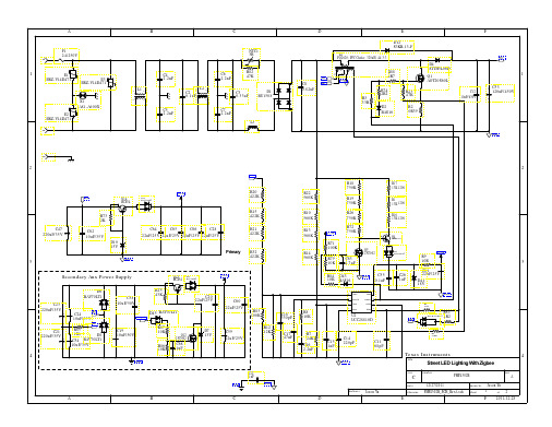
2)将连续传导模式(CCM)平均电流型控制PFC控制器和峰值电流模式PWM 级电路集成在同一芯片上,设计新颖,结构紧凑,如图1所示。
3)PFC控制器中的三输入高度线性化的乘法器和跨导(gm)电压误差放大器大大地提高了电路的瞬变响应。
4)PWM控制器最大占空比可编程设定,并且开关频率f PWM可以与f PFC相同,也可以选择f PWM=2f PFC,具体如表1所列。
5)为了减小PFC升压预调节器输出电容器上的纹波电流,PFC和PWM级分别采用前沿调制和后沿调制。
图2示出了UCC28510系列脉冲前沿/后沿调制(LEM/TEM)控制器与传统后沿/后沿调制( TEM/TEM)PFC与PWM组合控制器在能量贮存电容器(C ES)上的电流(i ES)对比。
图1 UCC28510系列PFC/PWM控制器内部结构图2 前沿/后沿调制(LEM/TEM)纹波电流与后沿/后沿调制(TEM/TEM)比较此外,UCC28510系列PFC/PWM组合控制器还具有可编程软启动,PFC输入电压前馈控制,峰值电流和功率限制,零功率检测和过电压保护等特征。
表1 UCC28510系列ICs之间的主要不同点3 应用电路及设计3.1 应用电路UCC2851X作为控制器的PFC升压预变换器与回扫(反激)式PWM功率级SMPS 电路如图3所示。
图中,UCC2851X(U1)中的PFC控制器、升压电感器L1、PFC 开关(Q1)、升压二极管D3和输出电容器C1等,组成有源PFC升压预变换器。
R3和R4组成的电阻分压器用作PFC变换器DC输出电压(400V)检测,感测信号通过U1的脚3输入到内部以7.5V为参考的误差放大器。
正比于整流电压的电流信号经电阻R1和U1的IAC脚(脚18)输入到内部乘法器,以保证整流器(D1)输入端的AC电流跟踪AC线路电压瞬时变化轨迹。
电阻R2是PFC级电流感测元件。
R2上感测的电压信号分别经U1脚16(ISENSE1)和脚14(PKLMT)输入到内部电流放大器和PFC电流限制比较器,以履行PFC级PWM脉冲占空比控制和峰值电流控制。
图3 UCC2851X典型应用电路R6和C3是U1启动元件。
当U1被启动Q1开始开关之后,变压器T1的辅助绕组、二极管D5和电容C3组成的电源电路为U1提供工作电压(和电流)。
U1脚2(RT)外部电阻R20用作设定振荡器频率。
U1脚4外部R16和R19组成的电阻分压器,用作编程PWM最大占空比。
电阻R5为PWM级电流感测元件。
R2上感测的电压信号经U1脚8(ISENSE2)输入,以履行峰值电流限制。
U1脚13(SS2)外部电容C5,用作编程PWM级栅极驱动软启动持续时间。
SMPS次级DC输出到初级的反馈环路,由电阻分压器、作为误差放大器使用的U3(TL431)和光耦合器U2组成。
U1的脚7(VERR)接收反馈信号,以控制PWM占空比。
3.2 主要元件参数确定的方法3.2.1 设计程序设计程序参考图3所示的应用电路。
首先选择UCC28510系列ICs中的一种控制器,再按以下步骤进行设计:1)功率级元器件;2)PFC级控制元件;3)PWM级控制元件。
元件的确定必须根据给定的技术条件,具体包括系统输出电压V OUT、输出功率P OUT和AC线路电压V AC范围。
其它的技术要求有效率和允许的电流谐波等。
3.2.2 确定相关参数1)PFC级最小占空比D1(min)PFC升压变换器在CCM下操作,最小占空比由最低AC线路电压V AC(min)和PFC 输出存储电容C1上的电压V C1决定。
D1(min)=1-(1)2)确定调节常数K1R能量存储电压的调节常数K1R由式(2)确定。
K1R=(2)式中:PWM导通参考是6.75V,PWM滞后为1.45V或3.2V,V REF=7.5V。
因此可得 K1R=0.29(对应UCC28510/28511/28514/28515);K1R=0.53(对应UCC28512/28513/28516/28517)。
3)最低能量存储电压V C1(min)C1上的最低能量存储电压V C1(min)由K1R和正常状态下C1上的电压V C1(nom)决定。
V C1(min)=(1-K1R)·V C1(nom)(3)4)编程PWM级开关频率f s(PWM)用U1脚RT外部电阻R20设定f s(PWM)R20=(4)推荐R20=45~500kΩ。
3.2.3 元器件的确定1)功率级元器件在图3所示的电路中,功率级元器件包括C1~C3、D1~D5、L1、R1、Q1、Q2和T1。
因篇幅所限,PWM功率级元器件Q2、D4、D5、C2和变压器T1不在此讨论。
在PFC级元器件C1、C3、D1~D3和Q1中,除C1因PFC/PWM同步化要求需要讨论外,其它元器件选择方法在固定频率PFC设计中都有介绍,故也不再涉及。
(1)升压电感器L1PFC升压电感器L1可利用式(5)计算。
L1=(5)式中:T S(PFC)为开关周期;P IN为输入功率;K RF=Δi L1(p-p)/i L1(max)=0.2~0.3,为纹波因数。
(2)电流传感电阻R2和PFC峰值电流限制编程电阻R17与R14PFC级电流感测电阻R2可由式(6)确定。
R2=(6)在式(6)中,R2操作动态范围V DYNAMIC围绕1V,i L1(max)=P IN/V AC(min)。
UCC2851X脚PKLMT外部电阻分压器R7与R14用作编程过电流门限电压。
R14可围绕10kΩ选择,R7与R14之间关系如下。
=(7)(3)电容器C1PFC升压变换器输出电容器C1的选择必须保证要求的支持(hold-up)时间t HU,其容值由式(8)确定。
C1=(8)C1还必须能经受住有效值纹波电流I C1(rms)。
I C1(rms)取决于开关Q2的电流I Q2、占空比D2(nom)、V C1(nom)和V AC(min)。
<(9)I C1(rms)与I Q2之比率可以从UCC2851X的相关曲线上查出。
(4)PWM级电流感测电阻R5UCC2851X脚8内部峰值电流限制比较器的输入门限电压V TH为1.3V,R5可按式(10)计算。
R5=V TH(1.3V)/i Q2(peak)(10)2)PFC级控制元件(1)乘法器动态范围设定乘法器动态范围依赖于PFC/PWM组合控制器IAC、VAOUT和VFF脚上的电流或电压。
这几个参数的限制条件如下:0≤i IAC(t)≤500μA(11)0≤V VOUT(t)≤5V1.4V≤V VFF≤V REF-1.4V相关元件的选择如表2所列。
表2 乘法器相关元件计算公式(2)PFC电流环路控制元件在U1的电流放大器输出(脚15)与电流放大器反相输入端(脚17)之间,在外部连接由C7和C6、R13组成的补偿网络。
R13用作设定在交叉频率f CO(PFC)上补偿器增益,选择C6在交叉频率上设置一个零点,C7用作在开关频率f S(PWM)的1/2处提供一个极点。
这三个元件的计算公式如表3所列。
表3 PFC电流环路控制元件计算公式3)PWM级控制元件U1脚4外部电阻R16和R19,用作设定最大占空比D PWM(max),以防止变压器饱和。
R16与R19之比由式(12)确定。
=-1(12)当脚4上电压为V DX时,最大占空比D PWM(max)可由式(13)计算。
D PWM(max)=(0.26-4.4×10⁻⁸f s)V DX+6.9×10⁻⁸f s-0.31(13)当V DX=4.15V时,D PWM(max)=(75±5)%。
它比PFC级最大占空比D PFC(max)〔95±5)%〕小一些。
4)元器件选择举例对于图3所示的应用电路,若AC输入范围为85~265V,PFC级电路DC输出电压是400V,输出功率为100W,U1选用UCC28517(f PFC=1/2f PWM),V CC脚电源12V,PFC级和变压器初级PWM级电路主要元器件的选择如下:(1)功率器件和磁性元件Q1和Q2选用IRFP450型MOSFET,D1选用PB66全桥整流器,D2选用G1756二极管,D3选用HFA08TB60快速恢复二极管。
升压电感器L1电感值为1.7mH,变压器T1选用PB2039。
(2)阻容元件主要阻容元件数值如表4所列。
表4 阻容元件的选择。