FPGA扩展板1-YQS
- 格式:pdf
- 大小:419.41 KB
- 文档页数:1
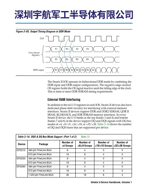
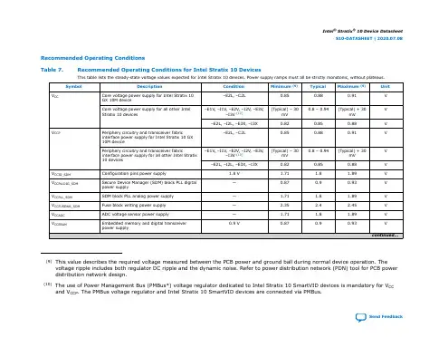
Figure2–55.Output TIming Diagram in DDR ModeThe Stratix II IOE operates in bidirectional DDR mode by combining theDDR input and DDR output configurations. The negative-edge-clockedOE register holds the OE signal inactive until the falling edge of the clock.This is done to meet DDR SDRAM timing requirements.External RAM InterfacingIn addition to the six I/O registers in each IOE, Stratix II devices also havededicated phase-shift circuitry for interfacing with external memoryinterfaces. Stratix II devices support DDR and DDR2 SDRAM, QDR IISRAM, RLDRAM II, and SDR SDRAM memory interfaces. In everyStratix II device, the I/O banks at the top (banks 3 and 4) and bottom(banks 7 and 8) of the device support DQ and DQS signals with DQ busmodes of ×4, ×8/×9, ×16/×18, or ×32/×36. Table2–14 shows the numberof DQ and DQS buses that are supported per device.Table2–14.DQS & DQ Bus Mode Support(Part 1 of2)Note(1)Device Package Number of×4GroupsNumber of×8/×9 GroupsNumber of×16/×18 GroupsNumber of×32/×36 GroupsEP2S15484-pin FineLine BGA8400 672-pin FineLine BGA18840 EP2S30484-pin FineLine BGA8400 672-pin FineLine BGA18840 EP2S60484-pin FineLine BGA8400 672-pin FineLine BGA188401,020-pin FineLine BGA361884I/O StructureTable 2–15 shows the possible settings for the I/O standards with drive strength control.Open-Drain OutputStratix II devices provide an optional open-drain (equivalent to an open-collector) output for each I/O pin. This open-drain output enables the device to provide system-level control signals (e.g., interrupt and write-enable signals) that can be asserted by any of several devices.Bus HoldEach Stratix II device I/O pin provides an optional bus-hold feature. The bus-hold circuitry can weakly hold the signal on an I/O pin at itslast-driven state. Since the bus-hold feature holds the last-driven state of the pin until the next input signal is present, you do not need an external pull-up or pull-down resistor to hold a signal level when the bus is tri-stated.Table 2–15.Programmable Drive Strength Note (1)I/O StandardI OH / I OL Current Strength Setting (mA) for ColumnI/O PinsI OH / I OL Current Strength Setting (mA) for Row I/OPins3.3-V LVTTL 24, 20, 16, 12, 8, 412, 8, 43.3-V LVCMOS 24, 20, 16, 12, 8, 48, 42.5-V LVTTL/LVCMOS 16, 12, 8, 412, 8, 41.8-V LVTTL/LVCMOS 12, 10, 8, 6, 4, 28, 6, 4, 21.5-V LVCMOS 8, 6, 4, 24, 2SSTL-2 Class I 12, 812, 8SSTL-2 Class II 24, 20, 1616SSTL-18 Class I 12, 10, 8, 6, 410, 8, 6, 4SSTL-18 Class II 20, 18, 16, 8-HSTL-18 Class I 12, 10, 8, 6, 412, 10, 8, 6, 4HSTL-18 Class II 20, 18, 16-HSTL-15 Class I 12, 10, 8, 6, 48, 6, 4HSTL-15 Class II 20, 18, 16-Note to Table 2–15:(1)The Quartus II software default current setting is the maximum setting for each I/O standard.The bus-hold circuitry also pulls undriven pins away from the input threshold voltage where noise can cause unintended high-frequency switching. You can select this feature individually for each I/O pin. The bus-hold output drives no higher than V CCIO to prevent overdriving signals. If the bus-hold feature is enabled, the programmable pull-up option cannot be used. Disable the bus-hold feature when the I/O pin has been configured for differential signals.The bus-hold circuitry uses a resistor with a nominal resistance (R BH) of approximately 7 kΩ to weakly pull the signal level to the last-driven state. See the DC & Switching Characteristics chapter in the Stratix II Device Handbook, Volume 1, for the specific sustaining current driven through this resistor and overdrive current used to identify the next-driven input level. This information is provided for each V CCIO voltage level.The bus-hold circuitry is active only after configuration. When going into user mode, the bus-hold circuit captures the value on the pin present at the end of configuration.Programmable Pull-Up ResistorEach Stratix II device I/O pin provides an optional programmablepull-up resistor during user mode. If you enable this feature for an I/O pin, the pull-up resistor (typically 25 kΩ) weakly holds the output to the V CCIO level of the output pin’s bank.Programmable pull-up resistors are only supported on user I/O pins, and are not supported on dedicated configuration pins, JTAG pins or dedicated clock pins.Advanced I/O Standard SupportStratix II device IOEs support the following I/O standards:■ 3.3-V LVTTL/LVCMOS■ 2.5-V LVTTL/LVCMOS■ 1.8-V LVTTL/LVCMOS■ 1.5-V LVCMOS■ 3.3-V PCI■ 3.3-V PCI-X mode 1■LVDS■LVPECL (on input and output clocks only)■HyperTransport technology■Differential 1.5-V HSTL Class I and II■Differential 1.8-V HSTL Class I and II■Differential SSTL-18 Class I and II■Differential SSTL-2 Class I and IIFor JTAG chains, the TDO pin of the first device drives the TDI pin of the second device in the chain. The V CCSEL input on JTAG input I/O cells (TCK , TMS , TDI , and TRST ) is internally hardwired to GND selecting the 3.3-V/2.5-V input buffer powered by V CCPD . The ideal case is to have the V CCIO of the TDO bank from the first device to match the V CCSEL settings for TDI on the second device, but that may not be possible depending on the application. Table 2–20 contains board design recommendations to ensure proper JTAG chain operation.Table 2–19.Board Design Recommendations for nCEO nCE Input Buffer Power in I/OBank 3Stratix II nCEO V CCIO Voltage Level in I/O Bank 7V C C I O = 3.3 V V C C I O =2.5 V V C C I O =1.8 V V C C I O =1.5 V V C C I O =1.2 V VCCSEL high(V C C I O Bank 3 = 1.5 V)v (1), (2)v (3), (4)v (5)v vVCCSEL high(V C C I O Bank 3 = 1.8 V)v (1), (2)v (3), (4)v vLevel shifter requiredVCCSEL low(nCE Powered by V C C P D = 3.3V)vv (4)v (6)Level shifter required Level shifter requiredNotes to Table 2–19:(1)Input buffer is 3.3-V tolerant.(2)The nCEO output buffer meets V O H (MIN) = 2.4 V .(3)Input buffer is 2.5-V tolerant.(4)The nCEO output buffer meets V OH (MIN) = 2.0 V .(5)Input buffer is 1.8-V tolerant.(6)An external 250-Ω pull-up resistor is not required, but recommended if signal levels on the board are not optimal.Table 2–20.Supported TDO/TDI Voltage Combinations (Part 1 of 2)DeviceTDI InputBuffer Power Stratix II TDO V C C I O Voltage Level in I/O Bank 4VC C I O = 3.3 V V C C I O = 2.5 V V C C I O = 1.8 V V C C I O = 1.5 V V C C I O = 1.2 VStratix IIAlwaysV C C P D (3.3V)v (1)v (2)v (3)Level shifter required Level shifter required。
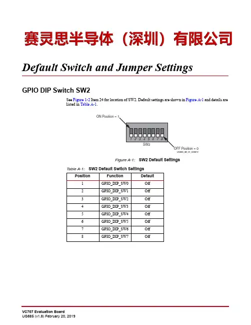
Default Switch and Jumper SettingsGPIO DIP Switch SW2See Figure 1-2 Item 24 for location of SW2. Default settings are shown in Figure A-1 and details are listed in Table A-1.Figure A-1:SW2 Default SettingsTable A-1:SW2 Default Switch SettingsPositionFunction Default 1GPIO_DIP_SW0Off 2GPIO_DIP_SW1Off 3GPIO_DIP_SW2Off 4GPIO_DIP_SW3Off 5GPIO_DIP_SW4Off 6GPIO_DIP_SW5Off 7GPIO_DIP_SW6Off 8GPIO_DIP_SW7OffAppendix A:Default Switch and Jumper SettingsConfiguration DIP Switch SW11See Figure 1-2 Item 29 for location of SW11. Default settings are shown in Figure A-2 and details are listed in Table A-2.The default mode setting M[2:0]=010 selects Master BPI configuration at board power-on.Default Jumper SettingsSee Figure A-3 for locations of jumpers listed in Table A-3.Figure A-2:SW11 Default SettingsTable A-2:SW11 Default Switch SettingsPositionFunctionDefault 1FLASH_A25A25Off 2FLASH_A24A24Off 3FPGA_M2M0Off 4FPGA_M1M1On 5FPGA_M0M3OffTable A-3:Default Jumper Settings Callout Jumper FunctionDefault JumperPositionSchematic0381418 PageNumber1J6SFP EnableNone 312J9XADC GND ferrite filter bypass jumper None 403J10XADC GND-to-XADC_AGND jumper 1–2404J11TI Controller U42 Addr 52 Reset jumper None 465J12TI Controller U43 Addr 53 Reset jumper None 506J13USB Mini-B Connector J2 VBUS None 447J14USB SMBC U8 CLKOUT selectorNone 448J38SFP RX Rate: 1-2=Full BW Rate, 2-3=Low BW Rate 1–2319J39SFP TX Rate: 1-2=Full BW Rate, 2-3=Low BW Rate 1–23110J42XADC external 1.2V or internal VREFP selector1–240Feature Descriptions For external measurements an XADC header (J19) is provided. This header can be used to provide analog inputs to the FPGA's dedicated VP/VN channel, and to the V AUXP[0]/V AUXN[0],V AUXP[8]/V AUXN[8] auxiliary analog input channels. Simultaneous sampling of Channel 0 and Channel 8 is supported.A user-provided analog signal multiplexer card can be used to sample additional external analog inputs using the 4 GPIO pins available on the XADC header as multiplexer address lines.Figure1-35 shows the XADC header connections.Figure 1-35:XADC Header (J19)Chapter 1:VC707 Evaluation Board FeaturesConfiguration OptionsThe FPGA on the VC707 board can be configured by the following methods:•Master BPI (uses the Linear BPI Flash).•JTAG (uses the USB-to-JTAG Bridge or Download cable). See USB JTAG for more informationSee 7Series FPGAs Configuration User Guide (UG470) [Ref 3] for further details on configuration modes.The method used to configure the FPGA is controlled by the mode pin (M2, M1, M0) settings selected through DIP switch SW11. Table 1-34 lists the supported mode switch settings.Figure 1-36 shows mode switch SW13.The mode pins settings on SW11 determine if the Linear BPI Flash is used for configuring the FPGA. DIP switch SW11 also provides the upper two address bits for the Linear BPI Flash and can be used to select one of multiple stored configuration bitstreams. Figure 1-37 shows the connectivity between the onboard nonvolatile Flash devices used for configuration and the FPGA.To obtain the fastest configuration speed an external 80MHz oscillator is wired to the EMCCLK pin of the FPGA. This allows users to create bitstreams that configure the FPGA over the 16-bit datapath from the Linear BPI Flash memory at a maximum synchronous read rate of 80MHz.Table 1-34:Mode Switch SW11 SettingsMode Pins (M2, M1, M0)Configuration Mode010Master BPI 101JTAGFigure 1-36:Mode SwitchConfiguration OptionsFigure 1-37:VC707 Board Configuration Circuit。
高性能软件无线电平台X6-面向高性能SoC验证和科学仿真主要特性支持PCI Express® Gen2 ×8 (但IP另配)搭载DDR3 SDRAM SO-DIMM系统搭载FMC连接器,可使用大部分RocketI/O(GTX)利用FMC可选基板能够对应各种接口提供PCI Express和DMA等参考设计无限扩展行业应用下一代软件无线电平台微软研究院软件无线电(Sora)是一种新型基于PC 的可编程无线电平台架构。
Sora 结合了可编程性和通用处理器(GPP )平台的性能和灵活性,同时使用的硬件和软件技术,以满足高性能的无线通信算法的计算挑战。
Sora 平台提供 Soft WiFi 开源代码。
SoftWiFi 目前支持率的802.11a/b/g 全部协议,无缝地与商业802.11网卡实现互操作,并达到商业网卡相当的性能。
Sora 是第一平台真正的软件无线电平台,支持用户开发的802.11a/b/g ,如物理层和MAC ,软件完全是标准PC 架构。
典型应用:White SpacesMobile PhonesPublic Safety RadioLand MobileBroadcast TV and FM RadioSatellite navigationCovers 6 Amateur Radio Bands射频部分主要特性:Dull-duplex Transceiver50 MHz to 5.8 GHz coverage50-100mW (17-20dBm) from 50 MHz to 1.2 GHz30-70mW (15-18dBm) from 1.2 GHz to 2.2 GHz25+ dB Output power control range under software controlReceive Specs:Noise figure of 5-7 dBIIP3 of 5-10 dBm;IIP2 of 40-55 dBm全频带射频收发模块实验十九双口RAM仿真实验一实验目的1 设计实验了解片内双口RAM的时序特性;2练习使用Modelsim编译及仿真功能;3 熟悉Dual-port RAM IP核的使用。
2.Stratix ArchitectureFunctional Description Stratix® devices contain a two-dimensional row- and column-based architecture to implement custom logic. A series of column and row interconnects of varying length and speed provide signal interconnects between logic array blocks (LABs), memory block structures, and DSP blocks.The logic array consists of LABs, with 10 logic elements (LEs) in each LAB. An LE is a small unit of logic providing efficient implementation of user logic functions. LABs are grouped into rows and columns across the device.M512 RAM blocks are simple dual-port memory blocks with 512 bits plus parity (576 bits). These blocks provide dedicated simple dual-port or single-port memory up to 18-bits wide at up to 318MHz. M512 blocks are grouped into columns across the device in between certain LABs.M4K RAM blocks are true dual-port memory blocks with 4K bits plus parity (4,608 bits). These blocks provide dedicated true dual-port, simple dual-port, or single-port memory up to 36-bits wide at up to 291MHz. These blocks are grouped into columns across the device in between certain LABs.M-RAM blocks are true dual-port memory blocks with 512K bits plus parity (589,824bits). These blocks provide dedicated true dual-port, simple dual-port, or single-port memory up to 144-bits wide at up to 269MHz. Several M-RAM blocks are located individually or in pairs within the device’s logic array.Digital signal processing (DSP) blocks can implement up to either eight full-precision 9×9-bit multipliers, four full-precision 18 × 18-bit multipliers, or one full-precision 36×36-bit multiplier with add or subtract features. These blocks also contain 18-bit input shift registers for digital signal processing applications, including FIR and infinite impulse response (IIR) filters. DSP blocks are grouped into two columns in each device.Each Stratix device I/O pin is fed by an I/O element (IOE) located at the end of LAB rows and columns around the periphery of the device. I/O pins support numerous single-ended and differential I/O standards. Each IOE contains a bidirectional I/O buffer and six registers for registering input, output, and output-enable signals. When used withStratix Device Handbook, Volume 1Stratix ArchitectureFigure 2–7.LE in Dynamic Arithmetic ModeStratix Device Handbook, Volume 1MultiTrack InterconnectTable 2–2 shows the Stratix device’s routing scheme.Table 2–2.Stratix Device Routing SchemeSourceDestinationL U T C h a i nR e g i s t e r C h a i nL o c a l I n t e r c o n n e c tD i r e c t L i n k I n t e r c o n n e c tR 4 I n t e r c o n n e c tR 8 I n t e r c o n n e c tR 24 I n t e r c o n n e c tC 4 I n t e r c o n n e c tC 8 I n t e r c o n n e c tC 16 I n t e r c o n n e c tL EM 512 R A M B l o c kM 4K R A M B l o c kM -R A M B l o c kD S P B l o c k sC o l u m n I O E R o w I O ELUT Chain v Register Chain v LocalInterconnect vvvvvvvDirect Link Interconnect v R4 Interconnect v vvvvR8 Interconnect vvvR24Interconnect vvv v C4 Interconnect v vvC8 Interconnect vvvC16Interconnect vvv vLEvvv v v v v v M512 RAM Blockv v v v v v M4K RAM Block v v v v v v M-RAM Block v v DSP Blocks vv vv v v Column IOE v v v v Row IOEvvvvvvStratix Device Handbook, Volume 1Stratix ArchitectureTriMatrix MemoryTriMatrix memory consists of three types of RAM blocks: M512, M4K, and M-RAM blocks. Although these memory blocks are different, they can all implement various types of memory with or without parity,including true dual-port, simple dual-port, and single-port RAM, ROM, and FIFO buffers. Table 2–3 shows the size and features of the different RAM blocks.Table 2–3.TriMatrix Memory Features (Part 1 of 2)Memory FeatureM512 RAM Block (32×18Bits)M4K RAM Block (128×36Bits)M-RAM Block (4K ×144Bits)Maximum performance (1)(1)(1)T rue dual-port memory vv Simple dual-port memoryv v v Single-port memoryvvvStratix Device Handbook, Volume 1TriMatrix MemoryConfigurations512×1256×2128×464×864×932×1632×184K ×12K ×21K ×4512×8512×9256×16256×18128×32128×3664K ×864K ×932K ×1632K ×1816K ×3216K ×368K ×648K ×724K ×1284K ×144Table 2–3.TriMatrix Memory Features (Part 2 of 2)Memory FeatureM512 RAM Block (32×18Bits)M4K RAM Block (128×36Bits)M-RAM Block (4K ×144Bits)。
zcusn10p1成分ZCU10P1 FPGA开发板结构ZCU10P1 FPGA开发板基于Xilinx Zynq UltraScale+ ZU10PC MPSoC器件构建,提供强大的处理和连接功能。
其结构包括以下主要组件:处理器子系统双核Arm Cortex-A53处理系统四核Arm Cortex-R5实时处理系统FPGA逻辑Xilinx UltraScale+ MPSoC FGPA,提供可编程逻辑阵列112,500个逻辑单元550个DSP切片1,920个I/O引脚存储器子系统512MB DDR4 SDRAM16MB QSPI闪存微型SD卡插槽连接性千兆以太网接口(RJ-45) USB 3.0接口HDMI接口DisplayPort接口其它特性4个PMOD接口,用于连接外围设备 JTAG编程接口电源开关和复位按钮散热器和风扇模块,用于散热管理尺寸和重量尺寸:240毫米 x 170毫米重量:约500克供电外部12V直流电源适配器设计工具Vivado Design SuitePetaLinux工具链应用ZCU10P1开发板广泛用于以下应用:人工智能和机器学习图像和视频处理车载系统通信和网络工业自动化优势高性能处理能力灵活的可编程FPGA逻辑丰富的连接选项紧凑型和低功耗广泛的应用程序支持结论ZCU10P1 FPGA开发板是一款功能强大且用途广泛的平台,为开发人员提供了创建创新和高效的嵌入式系统的基础。
其先进的特性和易用性使其成为需要高性能和灵活性的应用程序的理想选择。

Xilinx FPGA产品手册Xilinx FPGA Product Guide2023关于我们官方合作伙伴业务范围芯驿电子科技(上海)有限公司,成立于2012年,总部位于上海松江临港科技城,是一家车载智能产品和FPGA 技术方案公司,拥有“AUMO”和“ALINX”两大品牌,其中AUMO 品牌专注车载智能产品,ALINX 品牌专注于FPGA 产品和方案定制。
经历十年发展,公司产品已经远销海外30多个国家。
2018年,公司通过高新技术企业认证,并通过ISO9001质量体系认证;2019年,荣获上海市松江区九亭镇“科技创新奖”;2020年,荣获上海市“专精特新企业“称号;2021年,申请通过上海市科技型中小企业技术创新资金项目,通过了国家级科技型中小企业认定,并通过了高新技术企业认证复审;2022年获得上海市张江国家自主创新示范区专项发展资金并通过“上海市创新型中小企业”认证。
ALINX 是全球的FPGA 芯片龙头企业XILINX 官方合作伙伴,国内FPGA 芯片龙头企业紫光同创官方合作伙伴,同时作为百度AI 合作伙伴,为百度定制了国产AI飞桨系统的Edgeboard 系列边缘设备。
通过多年的研发投入,已经推出100多款FPGA SoM 模组和配套板卡,积累了1000多家企业批量用户,上万个独立开发者,市场占有率遥遥领先。
通过产品+定制化服务的经营方式,ALINX 将继续加大对产品研发和技术研究的投入,不断与垂直行业客户合作,聚焦高端设备领域,协助客户解决行业的技术难题。
主要聚焦于FPGA + AI 解决方案,FPGA 国产化,FPGA 开发套件, ALINX 自有品牌产品。
公司提供的设计解决方案涉及人工智能、自动驾驶、轨道交通、半导体、5G 通信、医疗设备、工业互联、仪器仪表、数据中心、机器视觉、视频图像处理等行业。
紫光同创国内唯一的FPGA 板卡官方合作伙伴,XILINX 官方重要合作伙伴,百度AI合作伙伴。
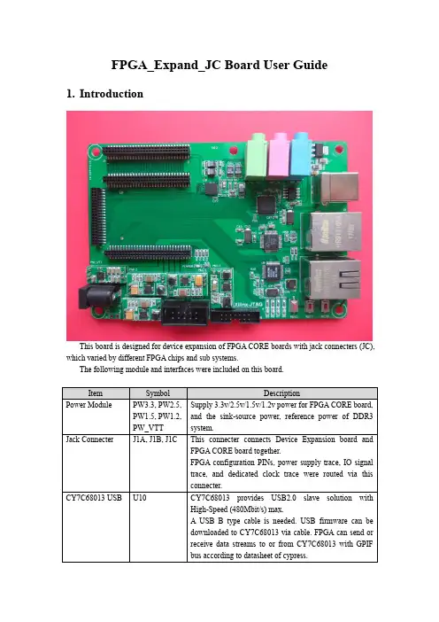
FPGA_Expand_JC Board User Guide1.IntroductionThis board is designed for device expansion of FPGA CORE boards with jack connecters (JC), which varied by different FPGA chips and sub systems.The following module and interfaces were included on this board.We have different versions of FPGA core board to adapt this board, and the pin assignments of FPGAs are different. Please take reference to the pin assignment file of each board individually. We use *.ucf file for Xilinx FPGAs and *.tcl file for Altera FPGAs to descript the relationship between FPGA pins, JC connector and signals/nets on device board. You can also take reference to the schematic of FPGA core board and FPGA expansion JC board to check this relationship. Pin assignment file and the schematic were located in directory schematic and pin.The FPGA example projects of this board are located in the directory examples/FPGA. Examples may have different versions sorted by different FPGA core board directories, but the function is the same. The following sections will use XC6SLX25 core board GF for example demonstration, to test the functions of hardware and coding. If you are using other board, just find out the corresponding projects in right directories. The operating order and the result are the same.A Keil uV2 projects for Cypress USB firmware was located in examples/Keil_uVision2 directory. This uV2 project is based on the 8051 core of CY7C68013A.A XCAP project for UDP pack generation was located in examples/XCAP directory.2.WM8731 Audio2.1.WM8731 LoopbackIn this Example, FPGA configure WM8731 via IIC, and then receive audio data streams from IIS bus. The receiving stream comes to a FIFO and then loopback to IIS bus.Open wm8731_test/WM8731_test.xise with ISE14.7, and compile this project to generate bit stream file. Then do the following steps.e an audio line to connect the board’s LINE_IN jack (J10) and your computer together.Run the audio player on your computer to generate music via the audio line.2.Download programming file to FPGA.3.Plug in your earphone or headphone to the board’s LINE_OUT jack (J12).4.You will hear the audio stream that comes from your earphone or headphone.2.2.Audio Record and PlayIn this Example, we can record the audio from LINE_IN jack and store the data streams to DDR/SDR SDRAM. Then, we can play the streams out to LINE_OUT jack.Open audio_record_play/audio_record_play.xise with ISE14.7, and compile this project to generate bit stream file. Then do the following steps.e an audio line to connect the board’s LINE_IN jack (J10) and your computer together.Run an audio player on your computer to generate music via the audio line.2.Download programming file to FPGA.3.Plug in your earphone or headphone to the board’s LINE_OUT jack (J12).4.Press KEY0, then you will find that LED0 light up, which means FPGA is storing audiostreams to SDRAM.5.Wait for about one minute or more (that depend on the depth of SDRAM and the samplerate), then press KEY0 again. You will find that LED0 is bland, which means FPGA is stopped to push audio streams to SDRAM. Another way, if you don’t press KEY0 in this step, LED0 will be turned off automatically when SDRAM is full.6.Press KEY1, then you will hear the audio stream that comes from your earphone orheadphone. At the same time, LED1 will light up until you press KEY1 again or the recorded audio stream is over.7.When recording audio stream, digital tube shows character ‘R’. When playing audiostream, digital tube shows character ‘P’.3.CY7C68013A USBIn this example, we use Cypress CyConsole to download HEX files to CY7C68013A, generate USB CMD and send the control streams to it. You need install the development kit first. Click tools/cy3684_ez_usb_fx2lp_development_kit_15.exe to install this software on your computer. To get familiar with Cypress USB Console, see Cypress USB Console Use’s Guide for details. You can find this file from the help menu of Cypress USB Console. There are many documents in the installation directory. If you want to know how to develop your USB system based on Cypress, please read the help files in <install_dir>\Cypress\USB\Help. There are also many example projects located at <install_dir>\Cypress\USB\Examples. The examples are Keil uVision2projects. This Cypress USB chip has an enhanced 8051 controller inside. Unzip <install_dir>\Cypress\USB\uV2_4k\Keil4KB_Cypress.zip to setup Keil uVision2. To develop your project on Keil uVision2, you should learn by yourself, or get more information from Internet.In slave_fifo_test.Uv2 project, we have configured 4 slave FIFOs of CY7C68013A. FIFOA, FIFOB, FIFOC and FIFOD prepared for EP2OUT, EP4OUT, EP6IN and EP8IN independently. EP2OUT and EP4OUT are the output endpoints of USB master, which means your computer in this example. EP6IN and EP8IN are input endpoints of USB master. As you know, USB master can send USB data to USB device via output endpoints and receive USB data from USB device via input endpoints. EP2OUT has 4 buffers, and each buffer is 512 Byte. EP6IN has 2 buffers and each buffer is 1024 Byte. EP4OUT and EP8IN have 2 buffers, and each buffer is 512 Byte. View the code of Keil uVision2 project for details.FPGA only use EP2OUT and EP6IN in this example. We can use our computer to send CMD to CY7C68013A via EP2OUT and receive DA TA from CY7C68013A via EP6IN. We haveor to the FIFOs. If EP2OUT’s FIFO has down stream data, FPGA read them out immediately and check whether it is a correct command. The invalid command will be discarded. When CMD_FF received, auto_upload_en comes to high. When CMD_00 received, auto_upload_en comes to low. If auto_upload_en is high, FPGA will send packs to EP6IN automatically when the FIFO is not full. Each pack is 1024 Byte, and has the same increasing data.Open cy7c68013a_test/cy7c68013a_test.xise with ISE14.7, and compile this project to generate bit stream file. Open slave_fifo_test.Uv2project with Keil uVision2, compile it to generate HEX file. Then do the following steps.1.Download the SOF file to FPGA.e an USB cable to connect the board and computer together. If this is the first time youconnect it to you computer, the system will inform you that a new USB device is found.After you have installed the USB driver, you will see the hardware information as following. (The driver will be automatically found in windows XP if you have installed Cypress USB Console. Otherwise, you should find the driver manually, please search the installation files in C:\Cypress\USB\Drivers. If you use Windows 7, please install the driver manually from tools/cypress_driver_for_win7when the operating system had found the new hardware.)3.Open Cypress USB Console to download the generated HEX file in step 4, as we can seefrom the following pictures.4.The download of HEX file will cause a USB reset, as we can see from the panel.5.Now, we send a 0xAAFF CMD to “Pipe 0: Endpoint 2 OUT”. Then, click “Bulk Trans”button to download them to CY7C68013A.6.The panel will show the following information.7.Change the pipe to “Pipe 2 : Endpoint 6 IN” , and click “Bulk Trans” to read back theupload data.8.You will find the following data in the panel. The total length is 1024 Byte, and the datais 0x00~0xFF, 0x00~0xFF, 0xFF~0x00, 0xFF~0x00.9.We can click “Bulk Trans” again, and we can receive another pack from the panel whichis the same with the previous one. Each time we click “Bulk Trans”, the same pack will come. Because the FPGA is sending upper stream packs continuously.10.Now, we send a 0xAA00 CMD to “Pipe 0: Endpoint 2 OUT”. Then, click “Bulk Trans”button to download them to CY7C68013A.11.Change the pipe to “Pipe 2: Endpoint 6 IN” , and click “Bulk Trans” to read back theupload data.12.You will find that you can only receive 4 packs from EP6. After that time, the consolereturned with failure.13.Why we can only receive four packs after the FPGA stop to upload upper stream data?Because EP6IN’s buffers can store two packs and FPGA’s buffer can store two packs.After the four packs been transferred via USB, no pack will be uploaded.14.Do step 5 to step 12 again and see what happens.4.SD Card TestIn this example, FPGA drives SD card in SPI mode and initialize it after power up. The flowing functions of SD card were supported.1.Single block read.2.Signal block write.3.Multiple block read.4.Multiple block write.5.Block erase and pre-erase.6.Get the CSD and CID register of SD card.In the test procedure descript in SD_Card_test_list.v, we have tested all the functions above and output the test result. This example treat SD card as a raw flash, on which file system is not supported. So, please backup all your files on SD card before this example.Before you test a SD card, please make sure that the content of this card is un-useable or you have finished the data back-up work, because this test may damage the file or file system of your SD card.Open sd_card_test/SD_Card_test.xise with ISE14.7, and compile this project to generate bit stream file. Then do the following steps.1.Insert SD card to socket U7.2.Download programming file to FPGA.3.The test program runs automatically after FPGA configuration because the reset pin andtest enable pin is high by default.4.You can see the test result. If LED1 is lighting up, it means that the test of SD card isfinished. If LED0 is lighting up, it means that error occurred during test.5.Button KEY0 means reset and active low. Button KEY1 means test enable and it activehigh. If you press KEY1 and then release it, a new test begins.5.W5500 EthernetIn this section, we will use Wireshark to monitor the packs on your computer, and XCAP to generate packs. Please install them first.The installation file of Wireshark is tools/Wireshark-win32-1.11.2.1339076454.exe,and the installation file of XCAP is tools/xcap.rar.The following examples use some private IPs, which protected by netlist file (*.ngc for Xilinx ISE, and *.qxp for Altera Quartus II). The IP can only works within 2 hours, for the purpose of demonstration or study. If you want to get rid of this limit or to get the source code and test bench file of IPs, please mail to dong_dt@ to buy the license.5.1.W5500 MACRAWIn this example, we only use W5500 as a MAC, and UDP solution were provided by FPGA. In order to test W5500’s MACRAW socket and the UDP function of FPGA, a self defined protocol over UDP is performed as following.1.IP address of computer is 192.168.7.200, IP address of board is 192.168.7.100.puter and board communicate with UDP.puter use UDP port 0x2018, and board use UDP port 0x2017.puter can send UDP packs to board, to read or write data from or to FPGA.5.To read register values from FPGA, UDP payload begins with byte 0x01, and the secondbyte is the register’s address. The following bytes were reserved.6.To write register data to FPGA, UDP payload begins with byte 0x02, and the second byteis the register’s address, the third byte is the writing data. The following bytes were reserved.7.The register map of FPGA is defined as following.Open w5500_macraw_test/w5500_macraw_test.xise with ISE14.7, and compile this project to generate bit stream file. Then do the following steps.1.Set the IP address of your computer as following.2.Download programming file to FPGA.3.Connect Ethernet cable between your computer and board with J3.4.Open Wireshark.exe, and select the local network of PC, and click the start button. Youcan see that Wireshark is displaying the Ethernet packs received on your computer, like the following picture.5.Start xcap.exe, and select “File -> open”, choose eth_test.xcap to open.6.In the following page, Select “Interafaces -> Refresh interfaces”, and then select the rightinterface of your network to “start interface”. You may have multiple Ethernet interfaces in your computer, like the second picture. I use “Interface2”to test W5500, but your selection may be different.7.Spread “Packet group”, and select “MY PACK”, and select “Interface2”. I use Interface2,but your selection may be different.The packs in window list were edited previously for this example. You can double click the packs, and view the content of packs.8.Select the pack with index 3 in XCAP, and set the Limit time as 1, then click the sendbutton as following picture. This pack means computer want to write 0x55 to FPGA’s register 0x01.9.You can find the pack sent from XCAP as the following picture.10.Select the pack with index 2 in XCAP, and then click the send button. This pack meanscomputer want to read data from FPGA’s register 0x01.11.You can see the following 3 packs in Wireshark as following. The first pack was sent byXCAP and the second pack was sent by board to give back the reading data 0x55 from register 0x01(see the green line in the second picture).12.Select packs with index 7, 8 and 9 in XCAP, and then click the send button. According theregister table introduced before, those pack set the timer in FPGA and make FPGA to senda UDP pack when timeout.13.You can see many UDP packs with user data block in Wireshark sent from board as thefollowing picture. The payload of UDP, consist a 4-Byte increasing sequence ID and256-Byte user data block.14.Select packs with index 10 in XCAP, and then click the send button. This pack write 0x00to FPGA’s register 0x82, will cause FPGA to stop sending UDP packs.15.In Wireshark, you will find that board stopped to send UDP packs with user data block. 5.2.W5500 UDP/TCPIn this example, we configured 3 socket of W5500. One socket is for UDP, one socket is forTCP client and one socket is for TCP server.Open w5500_udp_tcp_test/w5500_udp_tcp_test.xise with ISE14.7, and compile this project togenerate bit stream file. Then do the steps in the following section.5.2.1.W5500 UDP testThe steps to test UDP are the same with W5500 MACRAW test, shown in Chapter 5.1.5.2.2.W5500 TCP client testIn this test, W5500 acts as a TCP client and computer acts as a TCP server. After TCP link is established, if computer send string “START” to W5500 with TCP, W5500 begins to send TCP packs with user data block to computer when timeout. If computer send string “STOP ” to W5500 with TCP, W5500 stops to send TCP packs with user data block.Do the following steps.1.Open xcap.exe and select “Tools -> tcpudp”.2.In the following page, select “TCP” and set the values as following, then click “Listen”.3.In the following page, select “192.168.7.100:5001”.4.In the following page, type string “START” into dialog box, and click “Send” button.5.You can find that TCP packs were received from “Received” box as following. But it’shard to view the payload of TCP packs because this tool treats the payload as ASCII characters.6.However, we can use Wireshark to view TCP packs sent from W5500 as the followingpicture. The 4-Bytes sequence ID in the green outline increase pack after pack.7.Back to XCAP, in the following page, type string “STOP ”into dialog box, and click“Send” button. Attention that this string has 5 characters including space.8.You will find that board has stopped to send TCP packs with user data blocks.9.If you want to stop TCP connection, click “Close” button in the following page.5.2.3.W5500 TCP server testIn this test, W5500 acts as a TCP server and computer acts as a TCP client. After TCP link isestablished, if computer send string “START” to W5500 with TCP, W5500 begins to send TCPpacks with user data block to computer when timeout. If computer send string “STOP ” to W5500with TCP, W5500 stops to send TCP packs with user data block.Do the following steps.1.In the following page, select “TCP”and set the values as following, then click“Connect”.2.If connection is OK, IP address of W5500 and TCP port number will be shown inside thegreen outline in the picture. Then, type string “START” into dialog box, and click “Send”button.3.In Wireshark, you can see TCP packs sent from W5500 as the following picture. The4-Bytes sequence ID in the green outline increase pack after pack.4.Back to XCAP, in the following page, type string “STOP ”into dialog box, and click“Send” button. Attention that this string has 5 characters including space.5.You will find that board has stopped to send TCP packs with user data blocks.6.If you want to stop TCP connection, click “Close” button in the following page.6.RTL8211 EthernetIn this example, FPGA control and manage RTL8211CL with MDIO interface, and adapt RGMII 100M/1000M mode automatically. Above this PHY, FPGA have finished UDP transfer. In order to test RTL8211CL and the UDP function of FPGA, a self defined protocol over UDP is performed, with the same procedure of W5500 MACRAW test. Please refer to Chapter 5.1 for details.This examples use some private IPs, which protected by netlist file (*.ngc for Xilinx ISE, and *.qxp for Altera Quartus II). The IP can only works within 2 hours, for the purpose of demonstration or study. If you want to get rid of this limit or to get the source code and test bench file of IPs, please mail to dong_dt@ to buy the license.Open rtl8211_test/rtl8211_test.xise with ISE14.7, and compile this project to generate bit stream file. Then do the same steps in chapter 5.1, the only difference is that RTL8211CL use J2 to connect with computer.Generally, if one of the following cases happens, line speed is 100M.a.Ethernet cable is 4 wired, that only support 100M transfer.b.Your computer’s PHY have the max speed of 100M, or forced into 100M mode.c.RTL8211CL is forced into 100M mode.If both of the following cases happen, line speed is 1000M.a.Ethernet cable is 8 wired, that support 1000M transfer.b.Your computer’s PHY have the max speed of 1000M.c.Your computer and RTL8211CL works in auto negotiation mode, or forced into1000M mode.The negotiation speed of RTL8211CL is shown with LED[2:1]. 2’b00 means 10M, 2’b01 means 100M, 2’b10 means 1000M and 2’b11 is reserved.。
fpga工程师如何将扇出过大的信号分割成较小的信号, -回复FPGA(现场可编程逻辑门阵列)工程师在设计和开发电子系统时,经常会面临信号的扇出(Fan-out)过大的问题。
扇出过大的信号可能导致延迟、功耗和布局等方面的问题,因此需要将其分割成较小的信号。
本文将详细介绍FPGA工程师如何将扇出过大的信号分割成较小的信号,以及相关的方法和技巧。
第一步:了解信号扇出的问题在开始解决问题之前,FPGA工程师需要充分了解信号扇出的问题。
扇出是指一个信号驱动多个输入端口的能力,也就是说一个信号可能要同时连接到多个逻辑门或寄存器。
当扇出过大时,会产生以下问题:1. 延迟问题:由于信号要同时传输到多个逻辑门或寄存器,信号的传播延迟可能会增加,导致系统响应变慢。
2. 功耗问题:多个逻辑门或寄存器同时驱动一个信号,会产生大量的电流,增加系统的功耗。
3. 布局问题:扇出过大的信号可能需要经过长距离的布线,导致电路布局不合理,影响整体性能。
第二步:信号分割的方法在解决问题之前,我们需要确定信号分割的具体方法。
信号分割可以通过以下几种方式实现:1. 缓冲放大器(Buffer):使用缓冲放大器可以防止信号因为扇出过多而弱化,从而保持信号质量的稳定。
2. 梯形缓冲器(Schmitt Trigger):梯形缓冲器可以将输入信号的幅度进行适当的放大或缩小,以满足输出信号的需求。
3. 创建片选信号(Chip Select):对于需要同时驱动多个逻辑门或寄存器的信号,可以使用片选信号来选择对应的逻辑门或寄存器。
第三步:确定分割点确定信号分割的具体位置非常重要,它决定了信号的分割效果和系统性能。
以下是一些常见的确定分割点的方法:1. 状态机:对于复杂的信号处理需求,可以使用状态机来确定分割点。
状态机可以将输入信号的不同状态映射为不同的输出控制信号。
2. 分析电路结构:通过分析电路结构,可以确定信号分割的逻辑位置。
特别是在大型FPGA项目中,通过分析电路结构,可以找到大多数信号的分割位置。
FPGA(Field-Programmable Gate Array)作为一种可编程的逻辑器件,被广泛应用于数字信号处理、通信系统、嵌入式系统等领域。
在设计FPGA电路时,面积和速度是两个核心指标,对于设计人员来说,如何优化FPGA面积和速度是一个非常重要的课题。
本文将从面积优化和速度优化两个方面,探讨FPGA设计中的优化方法。
一、FPGA面积优化方法1. 逻辑优化在FPGA设计中,逻辑优化是一种常见的面积优化方法。
逻辑优化主要包括逻辑综合、布线和布局三个阶段。
在逻辑综合阶段,可以通过逻辑合并、功能分解等技术,减少逻辑门的数量,从而减小FPGA的面积占用。
在布线和布局阶段,可以通过合理的布线规则和布局布线策略,减少开关电路的数量,进而减小FPGA的面积占用。
2. 流水线技术流水线技术是一种常见的面积优化方法,通过将一个大模块分解成多个小模块,并将其连接成流水线,可以减小每个模块的逻辑规模,从而减小FPGA的面积占用。
流水线技术可以有效降低FPGA电路的逻辑深度,提高电路的运行速度。
3. 复用技术在FPGA设计中,复用技术是一种有效的面积优化方法。
通过设计可重用的功能模块,并在不同的部分中多次使用这些功能模块,可以减小FPGA的面积占用。
复用技术可以降低电路的逻辑规模,提高电路的复杂度。
4. 资源共享技术资源共享技术是一种常见的面积优化方法。
通过将同一类型的资源共享给多个功能模块使用,可以减小FPGA的资源占用。
资源共享技术可以降低FPGA的资源消耗,提高电路的资源利用率。
二、FPGA速度优化方法1. 时序优化时序优化是一种常见的速度优化方法。
通过优化时序约束、时钟分配等技术,可以降低电路的时序延迟,提高电路的工作速度。
时序优化可以通过同步技术和异步技术来实现,可以提高电路的工作速度。
2. 缓冲器插入技术缓冲器插入技术是一种有效的速度优化方法。
通过在关键路径上插入缓冲器,可以减小信号传输的延迟,提高电路的工作速度。
FPGA门级结构及其时序基础FPGA(Field Programmable Gate Array)是一种集成电路器件,它可以通过可编程逻辑门阵列和可编程互连器来实现特定电路的设计。
FPGA门级结构是指FPGA中各个逻辑门的组织方式。
这篇文章将介绍FPGA门级结构及其时序基础。
在FPGA中,逻辑门是组成各种逻辑功能的基本单元。
FPGA的门级结构通常是由LUT(Look-Up Table)、寄存器和互连器组成的。
LUT是FPGA中最基本的逻辑单元,它可以实现任意的逻辑函数。
寄存器用于存储逻辑电路中的状态信息,并可以控制数据的传输和执行时钟等操作。
互连器则负责将不同逻辑单元之间的信号连接起来,实现信号的传输和路由。
在FPGA中,时序是指电路中信号的传输和处理所需要的时间。
时序基础包括延迟、时钟和时序分析等概念。
延迟是指从信号输入到信号输出所需要的时间。
在FPGA门级结构中,由于信号需要经过多个逻辑门和互连器,所以会产生一定的延迟。
延迟的大小取决于逻辑门和互连器的特性以及信号路径的长度。
延迟的选择对于设计的性能和可靠性有着重要的影响。
如果延迟太大,会导致电路的响应较慢;如果延迟太小,会导致电路不稳定。
时钟是FPGA门级结构中非常重要的一个概念。
时钟是电路中的一个定时信号,它可以用于同步各个逻辑单元的操作。
在FPGA中,通常会提供多个时钟信号,以满足不同逻辑单元的时序需求。
时钟的频率决定了电路的工作速度,而时钟的相位决定了电路中各个操作的顺序和并行度。
时序分析是指对FPGA门级结构进行时序性能评估和验证的过程。
时序分析可以通过数学建模和仿真等方法来进行。
时序分析可以帮助设计者评估电路的工作速度、时序约束的满足程度以及时序故障等问题。
通过时序分析,设计者可以优化电路结构,提高电路的性能和可靠性。
总之,FPGA门级结构及其时序基础是FPGA设计的重要内容。
了解FPGA门级结构可以帮助设计者有效地利用FPGA资源,并优化电路结构。
Xilinx FPGA 引脚功能详细介绍注:技术交流用,希望对大家有所帮助。
IO_LXXY_# 用户10引脚XX代表某个Bank内唯一的一对引脚,Y=[P|N]代表对上升沿还是下降沿敏感,#代表bank 号2. IO_LXXY_ZZZ_# 多功能引脚ZZZ代表在用户10的基本上添加一个或多个以下功能。
Dn:I/O (在readback期间),在selectMAP或者BPI模式下,D[15:0]配置为数据口。
在从SelectMAP读反馈期间,如果RDWR_B=1,则这些引脚变成输出口。
配置完成后,这些引脚又作为普通用户引脚。
DO_DIN_MISO_MISO1 : I,在并口模式(SelectMAP/BPI )下,D0 是数据的最低位,在Bit-serial模式下,DIN是信号数据的输入;在SPI模式下,MISO是主输入或者从输出;在SPI*2或者SPI*4模式下,MISO1是SPI总线的第二位。
D1_MISO2,D2_MISO3 : I,在并口模式下,D1和D2是数据总线的低位;在SPI*4模式下,MISO2和MISO3是SPI总线的MSBs。
An : O, A[25:0]为BPI模式的地址位。
配置完成后,变为用户I/O 口。
AWAKE : O,电源保存挂起模式的状态输出引脚。
SUSPEND是一个专用引脚,AWAKE是一个多功能引脚。
除非SUSPEND模式被使能,AWAKE被用作用户I/O。
MOSI_CSI_B_MISO0 : I/O,在SPI模式下,主输出或者从输入;在SelectMAP模式下,CSI_B 是一个低电平有效的片选信号;在SPI*2或者SPI*4的模式下,MISOO是SPI总线的第一位数据。
FCS_B: O, BPI flash 的片选信号。
FOE_B : O, BPI flash的输出使能信号FWE_B : O, BPI flash的写使用信号LDC : O,BPI模式配置期间为低电平HDC : O,BPI模式配置期间为高电平CSO_B: O,在并口模式下,工具链片选信号。
《VF-Ti60F225-T产品手册》易灵思钛金16nm 60K FPGA开发板芯片介绍参数描述功能介绍尺寸介绍Demo介绍资料介绍套餐介绍实物演示u联系我们手册目录FPGA主芯片 系列介绍Trion系列FPGA40nm钛金系列FPGA16nm易灵思FPGAT20T35T55T85T120无DDR IP无MIPI CSI无DDR IP有MIPI CSI有DDR IP有MIPI CSI有DDR IP有MIPI CSI/DSI Ti35Ti60硬核DDR IP硬核MIPI IP Ti180Ti60F225I3 FPGA介绍供应商奥唯思 科技核心板型号VF-Ti60F225-CFPGA厂家易灵思(国产FPGA)钛金(Titanium) 系列FPGA型号Ti60F225I3FPGA资源60K 逻辑单元,集成DDR3/MIPI软核,160个DSP DDR3存储4G 16bit DDR3:K4B4G1646E PCBA尺寸40mm *40mmPCB工艺6层 1.6mm 沉金 绿色/亚黑板载FLASH 64Mbit SPI FLASH :W25Q64JWSSIQ 核心板外设1个USB供电口,8个测试LED2个用户按键,1个硬复位按键其他接口板载ZH1.25-6 JTAG下载口B2B接口2个0.5mm双排80P山谷道B2B接插件(母座*2)供电集成USB Mini供电口 | B2B接插件输入5V DC发烧设计,极致尺寸;工匠品质,为FPGA而生。
40m m40m mTi60F255I3易灵思FPGADCDC 电源模块8bit LED0.5mm双排80P 山谷道B2B接插件DDR3 16bit 4GbZH1.25-6JTAG下载口USB-Mini口仅供电24MHz晶振25MHz晶振2位用户按键64Mbit SPI-FLASH W25Q64JWSSIQ 1bit硬件复位按键【4*4cm极小尺寸】开供应商奥唯思 科技开发板型号VF-Ti60F225-TFPGA厂家易灵思(国产FPGA)钛金(Titanium) 系列FPGA型号Ti60F225I3FPGA资源60K 逻辑单元,集成DDR3/MIPI软核,160个DSP PCBA尺寸长 110mm * 宽 80mmPCB工艺4层 1.6mm 黑色 沉金 工艺核心板外设1)8个LED灯2)2个独立按键 + 1个硬复位按键3)1个ZH1.25-6 JTAG下载口底板外设1)1个USB串口(CH340N)2)DC3-40 40P 用户接口3)1路HDMI 1.4显示接口(FPGA驱动)4)1路LVDS LCD接口(1024*600显示屏)5)1路DVP相机接口(兼容奥唯思 科技所有DVP模组)6)1路MIPI RX接口(CSI/DSI 1.5Gbps)7)1路MIPI TX接口(CSI/DSI 1.5Gbps)备注MIPI RX+TX需要转接板16nm工艺,高速低功耗小尺寸FPGA u 集成DDR3/MIPI软核IPu 主打 MIPI CSI 1.5G 相机采集解决方案;u 主打 MIPI DSI 1.5G LCD显示解决方案;110mm80m mDVP摄像头接口(兼容奥唯思科技所有DVP相机)DCDC 电源模块1024x600LVDS LCD接口HDMI1.4接口4位用户独立按键USB串口(CH340N)IDC3-10JTAG下载口5V DC500供电接口电源开关DC3-40P用户接口(3.3V)8bit用户LED灯74HC595串转并驱动VF-Ti60F225-C 易灵思FPGA核心板MIPI TX/RX接口CSI/DSI 1.5GbpsFPGA开发板 尺寸/3D视图介绍FPGA开发板 基础Demo介绍分类工程名称FPGA工程介绍基础工程01_LED_8bit_Test LED流水灯测试实验(核心板)02_KEY_2bit_Test独立按键测试实验(核心板)03_FPGA_UART_Test_Bottom UART串口测试实验(底板)04_RGBLCD_Test_800480UART串口测试实验(底板)05_LVDS_LCD_Test_1024600800*480 RGB LCD屏幕显示实验05_MIPI_LCD_Test_10246001024*600 MIPI DSI屏幕显示实验07_Ti60_HDMI_1080P_Lvds_Test1920*1080@60 HDMI屏幕显示实验FPGA开发板 图像Demo介绍分类工程名称FPGA工程介绍图像工程01_Ti60_AR0135_HDMI_1280720基于AR0135 DVP相机的HDMI屏720P实时成像案例02_Ti60_AR0135_LCD-RGB_800480基于AR0135 DVP相机的RGB屏(800*480)实时成像案例03_Ti60_AR0135_LCD-LVDS_1024600基于AR0135 DVP相机的LVDS屏(1024*600)实时成像案例04_Ti60_AR0135_LCD-DSI_1024600基于AR0135 DVP相机的MIPI DSI屏(1024*600)实时成像案例05_Ti60_SC130GS_MIPIx4_HDMI_1280720基于SC130S MIPI 4lane相机的HDMI屏720P实时成像案例06_Ti60_SC130GS_MIPIx4_LCD-RGB_800480基于SC130S MIPI 4lane相机的RGB屏(800*480)实时成像案例07_Ti60_SC130GS_MIPIx4_LCD-LVDS_1024600基于SC130S MIPI 4lane相机的LVDS屏(1024*600)实时成像案例08_Ti60_SC130GS_MIPIx4_LCD-DSI_1024600基于SC130S MIPI 4lane相机的MIPI DSI屏(1024*600)实时成像案例完整的 MIPI CSI/DSI 解决方案,成熟的案例及量产经验!VF-Ti60F225易灵思FPGA主板FPGA下载器可选多种DVP模组SC130GS 彩色/黑白130万1/3寸1024*600 MIPI DSI液晶屏1024*600 LVDS液晶屏SC200AI 彩色200万1/3寸可选多种MIPI模组FPGA开发板 DVP/MIPI采集显示解决方案奥唯思FPGA官微奥唯思 技术支持官方网站: 资料下载: 官方淘宝: “奥唯思FPGA ” 店铺FPGA论坛: 851598171奥唯思FPGA交流群1。
Low Power Design with CoolRunner-II CPLDsClock DividerGlobal clock networks tend to be the largest power consuming elements in CPLDs. Any effortto reduce the frequency of the global clock network greatly benefits the system with respect topower consumption. Therefore, CoolRunner-II devices have been designed to include a clockdivider network on global clock, GCK2. Without introducing additional clock delays, the clockdivider has the capability of dividing the system clock by even integers ranging from 2 to 16, asshown in Figure1.Figure 1: Clock Division Circuitry for GCK2Some systems use state machines, for example, that do not require the full speed of theexternal system clock. A clock divider is the perfect tool to reduce system power in this case.The clock divider provides an excellent alternative to adding a user defined clock divider builtfrom logic, which would waste logic otherwise usable for more features in the design. A lowerfrequency on the global clock network, provided by the clock divider, will reduce the powerconsumed by the CoolRunner-II CPLD.Generally speaking, designing with the slowest system clock possible will reduce powerconsumption. To this end, the clock divider provided in the CoolRunner-II architecture willgreatly assist the designer.DualEDGE RegistersBy utilizing both edges of the clock signal, the macrocell can do twice the work when configuredas a DualEDGE flip-flop. Figure2 displays the macrocell configured as a DualEDGE flip-flop. Asystem without the aid of the DualEDGE flip-flop would need to provide a clock at twice thefrequency to obtain the same work output at the macrocell. Since the macrocells withDualEDGE flip-flops operate on both the rising and falling edges of the clock, the clock networkis used more efficiently. Consequently, power consumption is reduced when the global clocknet is operating at a lower frequency.Figure 2: Macrocell Clock Chain with DualEDGE Option ShownDualEDGE flip-flops further enhance the functional possibilities of the clock divider andtherefore improve power savings. The global clock can be effectively divided by odd integers of3, 5, and 7 if used with the DualEDGE flip-flop. For example, if a divide by 3 clock is desired forUsing CoolRunner-II Advanced FeaturesPullupThe internal pullup allows the designer to eliminate external pullup resistors on the board,thereby reducing cost and simplifying board layout. Table8 illustrates the attribute syntax forspecifying the pullup I/O termination.I/O Configuration CoolRunner-II devices support multiple I/O banks in a single device, allowing for easy interfacing to different voltage standards on one chip. A device can support one I/O standard per bank (i.e., XC2C128 has two banks and can therefore support up to two I/O standards). Regardless of which I/O voltage standard is selected, any pin may be configured as an open-drain output.I/O StandardsTable9 lists the supported I/O standards on CoolRunner-II devices. Note that all standards are not supported in every density.Table 8: Pullup AttributeAttributeFormat Syntax ExampleUCF NET <signal name> PULLUP;NET data_in PULLUP;NET clock PULLUP;ABEL XILINX PROPERTY 'PULLUP <signal name>';XILINX PROPERTY 'PULLUP data_in';XILINX PROPERTY 'PULLUP clock';VHDL attribute PULLUP : STRING;attribute PULLUP of <signal name>: signal is "TRUE";Note: The string attribute need only be declared once forall PULLUP attributes.attribute PULLUP : STRING;attribute PULLUP of data_in: signal is "TRUE"; attribute PULLUP of clock: signal is "TRUE";Verilog//SYNTHESIS attribute PULLUP of <signal name>;Note: The comment delimiters are intentional andnecessary for XST.//SYNTHESIS attribute PULLUP of data_in; //SYNTHESIS attribute PULLUP of clock;Table 9: CoolRunner-II Supported I/O StandardsXC2C32A XC2C64A XC2C128XC2C256XC2C384XC2C512 I/O Banks222244 LVTTL Yes Yes Yes Yes Yes Yes LVCMOS33,LVCMOS25,& LVCMOS18Yes Yes Yes Yes Yes Yes1.5V I/Os Yes Yes Yes Yes Yes YesSSTL2-1 &SSTL3-1No No Yes Yes Yes Yes HSTL-1No No Yes Yes Yes Yes。
Logos FPGA开发平台用户手册AXP12开发板2 / 39芯驿电子科技(上海)有限公司文档版本控制目录文档版本控制 (2)一、开发板简介 (5)二、FPGA核心板 (7)(一)简介 (7)(二)FPGA (8)(三)有源晶振 (10)(四)SDRAM (10)(五)QSPI Flash (13)(六)LED灯 (14)(七)扩展接口 (15)(八)电源 (18)(九)结构图 (20)三、扩展板 (21)(一)简介 (21)(二)千兆以太网接口 (22)(三)HDMI输出接口 (24)(四)USB2.0通信接口 (25)(五)SD卡槽 (27)(六)USB转串口 (28)(七)EEPROM 24LC04 (29)(八)实时时钟DS1302 (30)(九)扩展口 (31)(十)JTAG接口 (33)(十一)摄像头接口 (34)(十二)按键 (36)(十三)LED灯 (37)(十四)供电电源 (38)(十五)结构图 (39)3 / 394 / 39芯驿电子科技(上海)有限公司紫光同创Logos 系列的FPGA 开发平台(型号:AXP12)正式发布了,为了让您对此开发平台可以快速了解,我们编写了此用户手册。
这款 Logos 系列FPGA 开发平台采用核心板加扩展板的模式,方便用户对核心板的二次开发利用。
在底板设计上我们设计了丰富的外围接口,比如千兆以太网接口, HDMI 输出接口,USB2.0通信接口,Uart 通信接口,SD 卡接口,RTC 电路等等。
满足用户各种高速数据传输,视频图像处理和工业控制的要求,是一款"全能级“的FPGA 开发平台。
为高速视频传输,网络和USB 通信及数据处理的前期验证和后期应用提供了可能。
相信这样的一款产品非常适合从事FPGA 开发的学生、工程师等群体。
一、开发板简介在这里,对这款Logos FPGA开发平台进行简单的功能介绍。
开发板的整个结构,继承了我们一贯的核心板+扩展板的模式来设计的。