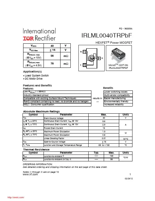
AD5721R;中文规格书,Datasheet资料
- 格式:pdf
- 大小:68.53 KB
- 文档页数:2


ALC5621I2S AUDIO CODEC + 1.3W CLASS AB/D MONO SPEAKER AMPLIFIERDATASHEETRev. 1.027 December 2007Track ID: JATR-1076-21Realtek Semiconductor Corp.No. 2, Innovation Road II, Hsinchu Science Park, Hsinchu 300, TaiwanTel.: +886-3-578-0211. Fax: +886-3-577-6047I S Audio Codec + 1.3W Class AB/D Mono Speaker Amplifierii Track ID: JATR-1076-21 Rev. 1.0COPYRIGHT ©2007 Realtek Semiconductor Corp. All rights reserved. No part of this document may be reproduced, transmitted, transcribed, stored in a retrieval system, or translated into any language in any form or by any means without the written permission of Realtek Semiconductor Corp.DISCLAIMERRealtek provides this document “as is”, without warranty of any kind, neither expressed nor implied, including, but not limited to, the particular purpose. Realtek may make improvements and/or changes in this document or in the product described in this document at any time. This document could include technical inaccuracies or typographical errors.TRADEMARKSRealtek is a trademark of Realtek Semiconductor Corporation. Other names mentioned in this document are trademarks/registered trademarks of their respective owners.USING THIS DOCUMENTThis document is intended for the hardware and software engineer’s general information on the Realtek ALC5621 Audio Codec IC.Though every effort has been made to ensure that this document is current and accurate, more information may have become available subsequent to the production of this guide. In that event, please contact your Realtek representative for additional information that may help in the development process. REVISION HISTORYRevision Release Date Summary1.0 2007/12/27 First releaseTable of Contents1.GENERAL DESCRIPTION (1)2.FEATURES (2)3.SYSTEM APPLICATIONS (2)4.BLOCK DIAGRAMS (3)4.1.F UNCTION B LOCK (3)4.2.A UDIO M IXER P ATH (4)5.PIN ASSIGNMENTS (5)5.1.G REEN P ACKAGE AND V ERSION I DENTIFICATION (5)6.PIN DESCRIPTIONS (6)6.1.D IGITAL I/O P INS (6)6.2.A NALOG I/O P INS (6)6.3.F ILTER/R EFERENCE (7)6.4.P OWER/G ROUND (7)7.FUNCTIONAL DESCRIPTION (8)7.1.P OWER (8)7.2.R ESET (8)7.2.1.Power-On Reset (POR) (8)7.3.C LOCKING (9)7.3.1.Phase-Locked Loop (9)7.3.2.I2C and Stereo I2S (10)7.4.D IGITAL D ATA I NTERFACE (11)7.4.1.Stereo I2S/PCM Interface (11)7.5.A UDIO D ATA P ATH (14)7.5.1.Vref (14)7.5.2.Stereo ADC (14)7.5.3.Stereo DAC (14)7.6.M IXERS (15)7.6.1.Headphone Mixer (15)7.6.2.MONO Mixer (16)7.6.3.Speaker Mixer (16)7.6.4.ADC Record Mixer (17)7.7.A NALOG A UDIO I NPUT P ATH (18)7.7.1.Line Input (18)7.7.2.AUXiliary Input (18)7.7.3.Microphone Input (18)7.8.A NALOG A UDIO O UTPUT D ATA P ATH (19)7.8.1.Speaker Output (19)7.8.2.Headphone Output (20)7.8.3.MONO Output (20)7.9.AVC C ONTROL (21)7.10.H ARDWARE S OUND E FFECTS (23)7.10.1.Equalizer Block (23)7.10.2.Pseudo Stereo and Spatial 3D Sound (23)7.11.I2C C ONTROL I NTERFACE (24)7.11.1.Addressing Setting (24)I S Audio Codec + 1.3W Class AB/D Mono Speaker Amplifier iii Track ID: JATR-1076-21 Rev. 1.0plete Data Transfer (24)7.12.O DD-A DDRESSED R EGISTER A CCESS (25)7.13.P OWER M ANAGEMENT (25)7.14.GPIO AND J ACK D ETECT F UNCTION (26)7.15.I NTERNAL E VENT S IGNAL I NTERRUPTS (27)7.16.H EADPHONE D EPOP (27)8.MIXER REGISTERS LIST (28)8.1.R EG-00H:R ESET (28)8.2.R EG-02H:S PEAKER O UTPUT V OLUME (28)8.3.R EG-04H:H EADPHONE O UTPUT V OLUME (29)8.4.R EG-06H:MONO_OUT/AUXOUT V OLUME (30)8.5.R EG-08H:AUXIN V OLUME (30)8.6.R EG-0A H:LINE_IN V OLUME (31)8.7.R EG-0C H:STEREO DAC V OLUME (31)8.8.R EG-0E H:MIC V OLUME (32)8.9.R EG-10H:MIC R OUTING C ONTROL (32)8.10.R EG-12H:ADC R ECORD G AIN (33)8.11.R EG-14H:ADC R ECORD M IXER C ONTROL (33)8.12.R EG-16H:A VOL S OFT V OLUME C ONTROL T IME (34)8.13.R EG-1C H:O UTPUT M IXER C ONTROL (34)8.14.R EG-22H:M ICROPHONE C ONTROL (35)8.15.R EG-34H:D IGITAL A UDIO I NTERFACE C ONTROL (35)8.16.R EG-36A H:S TEREO AD/DA C LOCK C ONTROL (36)8.17.R EG-38H:C OMPANDING C ONTROL (37)8.18.R EG-3A H:P OWER M ANAGEMENT A DDITION 1 (37)8.18.1.Headphone Output Amplifier Configuration (38)8.18.2.Auxiliary Output Amplifier Configuration (38)8.19.R EG-3C H:P OWER M ANAGEMENT A DDITION 2 (39)8.20.R EG-3E H:P OWER M ANAGEMENT A DDITION 3 (40)8.21.R EG-40H:A DDITIONAL C ONTROL R EGISTER (41)8.22.R EG-42H:G LOBAL C LOCK C ONTROL R EGISTER (42)8.23.R EG-44H:PLL C ONTROL R EGISTER (42)8.23.1.Reg-44h: PLL Control Register (42)8.23.2.PLL Clock Setting Table for 48K: (Unit: MHz) (43)8.23.3.PLL Clock Setting Table for 44.1K: (Unit: MHz) (43)8.24.R EG-4A H:GPIO_O UTPUT P IN C ONTROL (43)8.25.R EG-4C H:GPIO P IN C ONFIGURATION (44)8.26.R EG-4E H:GPIO P IN P OLARITY (44)8.27.R EG-50H:GPIO P IN S TICKY (45)8.28.R EG-52H:GPIO P IN W AKE-U P (45)8.29.R EG-54H:GPIO P IN S TATUS (46)8.30.R EG-56H:P IN S HARING (46)8.31.R EG-58H:O VER-C URRENT S TATUS (47)8.32.R EG-5A H:J ACK D ETECT C ONTROL R EGISTER (47)8.33.R EG-5E H:MISC C ONTROL (48)8.34.R EG-60H:S TEREO AND S PATIAL E FFECT B LOCK C ONTROL (49)8.35.R EG-62H:EQ C ONTROL (50)8.36.R EG-66H:EQ M ODE C HANGE E NABLE (51)8.37.R EG-68H:AVC C ONTROL (51)8.38.R EG-6A H:I NDEX A DDRESS (52)8.39.R EG-6C H:I NDEX D ATA (52)8.40.I NDEX-00H:EQ B AND-0C OEFFICIENT (LP0: A1) (52)8.41.I NDEX-01H:EQ B AND-0G AIN (LP0:H O) (52)8.42.I NDEX-02H:EQ B AND-1C OEFFICIENT (BP1: A1) (53)I S Audio Codec + 1.3W Class AB/D Mono Speaker Amplifier iv Track ID: JATR-1076-21 Rev. 1.08.43.I NDEX-03H:EQ B AND-1C OEFFICIENT (BP1: A2) (53)8.44.I NDEX-04H:EQ B AND-1G AIN (BP1:H O) (53)8.45.I NDEX-05H:EQ B AND-2C OEFFICIENT (BP2: A1) (53)8.46.I NDEX-06H:EQ B AND-2C OEFFICIENT (BP2: A2) (54)8.47.I NDEX-07H:EQ B AND-2G AIN (BP2:H O) (54)8.48.I NDEX-08H:EQ B AND-3C OEFFICIENT (BP3: A1) (54)8.49.I NDEX-09H:EQ B AND-3C OEFFICIENT (BP3: A2) (54)8.50.I NDEX-0A H:EQ B AND-3G AIN (BP3:H O) (55)8.51.I NDEX-0B H:EQ B AND-4C OEFFICIENT (HPF: A1) (55)8.52.I NDEX-0C H:EQ B AND-4G AIN (HPF:H O) (55)8.53.I NDEX-11H:EQ I NPUT V OLUME C ONTROL (55)8.54.I NDEX-12H:EQ O UTPUT V OLUME C ONTROL (56)8.55.I NDEX-21H:A UTO V OLUME C ONTROL R EGISTER 1 (56)8.56.I NDEX-22H:A UTO V OLUME C ONTROL R EGISTER 2 (56)8.57.I NDEX-23H:A UTO V OLUME C ONTROL R EGISTER 3 (56)8.58.I NDEX-24H:A UTO V OLUME C ONTROL R EGISTER 4 (57)8.59.I NDEX-25H:A UTO V OLUME C ONTROL R EGISTER 5 (57)8.60.I NDEX-39H:D IGITAL I NTERNAL R EGISTER (57)8.61.I NDEX-46H:C LASS D I NTERNAL R EGISTER (58)8.62.R EG-7C H:VENDOR ID1 (58)8.63.R EG-7E H:VENDOR ID2 (58)9.ELECTRICAL CHARACTERISTICS (59)9.1.DC C HARACTERISTICS (59)9.1.1.Absolute Maximum Ratings (59)9.1.2.Recommended Operating Conditions (59)9.1.3.Static Characteristics (59)9.2.A NALOG P ERFORMANCE C HARACTERISTICS (60)9.3.S IGNAL T IMING (62)9.3.1.I2C Control Interface (62)9.3.2.I2S Master Mode (63)9.3.3.I2S Slave Mode (64)10.APPLICATION CIRCUIT (65)11.MECHANICAL DIMENSIONS (66)12.APPENDIX A: STEREO I2S CLOCK TABLE (68)13.ORDERING INFORMATION (69)I S Audio Codec + 1.3W Class AB/D Mono Speaker Amplifier v Track ID: JATR-1076-21 Rev. 1.0List of TablesT ABLE 1.D IGITAL I/O P INS (6)T ABLE 2.A NALOG I/O P INS (6)T ABLE 3.F ILTER/R EFERENCE (7)T ABLE 4.P OWER/G ROUND (7)T ABLE 5.R ESET O PERATION (8)T ABLE 6.P OWER-O N R ESET V OLTAGE (8)T ABLE 7.C LOCK S ETTING T ABLE FOR 48K(U NIT:MH Z) (9)T ABLE 8.C LOCK S ETTING T ABLE FOR 44.1K(U NIT:MH Z) (10)T ABLE 9.MONO/AUXOUT O UTPUT S IGNAL T ABLE (20)T ABLE 10.A DDRESSING S ETTING (24)T ABLE 11.W RITE WORD P ROTOCOL (25)T ABLE 12.R EAD WORD P ROTOCOL (25)T ABLE 13.R EG-00H:R ESET (28)T ABLE 14.R EG-02H:S PEAKER O UTPUT V OLUME (28)T ABLE 15.R EG-04H:H EADPHONE O UTPUT V OLUME (29)T ABLE 16.R EG-06H:MONO_OUT/AUXOUT V OLUME (30)T ABLE 17.R EG-08H:AUXIN V OLUME (30)T ABLE 18.R EG-0A H:LINE_IN V OLUME (31)T ABLE 19.R EG-0C H:STEREO DAC V OLUME (31)T ABLE 20.R EG-0E H:MIC V OLUME (32)T ABLE 21.R EG-10H:MIC R OUTING C ONTROL (32)T ABLE 22.R EG-12H:ADC R ECORD G AIN (33)T ABLE 23.R EG-14H:ADC R ECORD M IXER C ONTROL (33)T ABLE 24.R EG-16H:A VOL S OFT V OLUME C ONTROL T IME (34)T ABLE 25.R EG-1C H:O UTPUT M IXER C ONTROL (34)T ABLE 26.R EG-22H:M ICROPHONE C ONTROL (35)T ABLE 27.R EG-34H:A UDIO I NTERFACE (35)T ABLE 28.R EG-36H:S TEREO AD/DA C LOCK C ONTROL (36)T ABLE 29.R EG-38H:C OMPANDING C ONTROL (37)T ABLE 30.R EG-3A H:P OWER M ANAGEMENT A DDITION 1 (37)T ABLE 31.H EADPHONE O UTPUT A MPLIFIER C ONFIGURATION (38)T ABLE 32.A UXILIARY O UTPUT A MPLIFIER C ONFIGURATION (38)T ABLE 33.R EG-3C H:P OWER M ANAGEMENT A DDITION 2 (39)T ABLE 34.R EG-3E H:P OWER M ANAGEMENT A DDITION 3 (40)T ABLE 35.R EG-40H:A DDITIONAL C ONTROL R EGISTER (41)T ABLE 36.R EG-42H:G LOBAL C LOCK C ONTROL R EGISTER (42)T ABLE 37.R EG-44H:PLL C ONTROL R EGISTER (42)T ABLE 38.PLL C LOCK S ETTING T ABLE FOR 48K:(U NIT:MH Z) (43)T ABLE 39.PLL C LOCK S ETTING T ABLE FOR 44.1K:(U NIT:MH Z) (43)T ABLE 40.R EG-4C H:GPIO_O UTPUT P IN C ONTROL (43)T ABLE 41.R EG-4C H:GPIO P IN C ONFIGURATION (44)T ABLE 42.R EG-4E H:GPIO P IN P OLARITY (44)T ABLE 43.R EG-50H:GPIO P IN S TICKY (45)T ABLE 44.R EG-52H:GPIO P IN W AKE-U P (45)T ABLE 45.R EG-54H:GPIO P IN S TATUS (46)T ABLE 46.R EG-56H:P IN S HARING (46)T ABLE 47.R EG-58H:O VER-C URRENT S TATUS (47)T ABLE 48.R EG-5A H:J ACK D ETECT C ONTROL R EGISTER (47)T ABLE 49.R EG-5E H:MISC C ONTROL (48)T ABLE 50.R EG-60H:S TEREO AND S PATIAL E FFECT B LOCK C ONTROL (49)T ABLE 51.R EG-62H:EQ C ONTROL (50)T ABLE 52.R EG-66H:EQ M ODE C HANGE E NABLE (51)I S Audio Codec + 1.3W Class AB/D Mono Speaker Amplifier vi Track ID: JATR-1076-21 Rev. 1.0T ABLE 53.R EG-68H:AVC C ONTROL (51)T ABLE 54.R EG-6A H:I NDEX A DDRESS (52)T ABLE 55.R EG-6C H:I NDEX D ATA (52)T ABLE 56.I NDEX-00H:EQ B AND-0C OEFFICIENT (LP0: A1) (52)T ABLE 57.I NDEX-01H:EQ B AND-0G AIN (LP0:H O) (52)T ABLE 58.I NDEX-02H:EQ B AND-1C OEFFICIENT (BP1: A1) (53)T ABLE 59.I NDEX-03H:EQ B AND-1C OEFFICIENT (BP1: A2) (53)T ABLE 60.I NDEX-04H:EQ B AND-1G AIN (BP1:H O) (53)T ABLE 61.I NDEX-05H:EQ B AND-2C OEFFICIENT (BP2: A1) (53)T ABLE 62.I NDEX-06H:EQ B AND-2C OEFFICIENT (BP2: A2) (54)T ABLE 63.I NDEX-07H:EQ B AND-2G AIN (BP2:H O) (54)T ABLE 64.I NDEX-08H:EQ B AND-3C OEFFICIENT (BP3: A1) (54)T ABLE 65.I NDEX-09H:EQ B AND-3C OEFFICIENT (BP3: A2) (54)T ABLE 66.I NDEX-0A H:EQ B AND-3G AIN (BP3:H O) (55)T ABLE 67.I NDEX-0B H:EQ B AND-4C OEFFICIENT (HPF: A1) (55)T ABLE 68.I NDEX-0C H:EQ B AND-4G AIN (HPF:H O) (55)T ABLE 69.I NDEX-11H:EQ I NPUT V OLUME C ONTROL (55)T ABLE 70.I NDEX-12H:EQ O UTPUT V OLUME C ONTROL (56)T ABLE 71.I NDEX-21H:A UTO V OLUME C ONTROL R EGISTER 1 (56)T ABLE 72.I NDEX-22H:A UTO V OLUME C ONTROL R EGISTER 2 (56)T ABLE 73.I NDEX-23H:A UTO V OLUME C ONTROL R EGISTER 3 (56)T ABLE 74.I NDEX-24H:A UTO V OLUME C ONTROL R EGISTER 4 (57)T ABLE 75.I NDEX-25H:A UTO V OLUME C ONTROL R EGISTER 5 (57)T ABLE 76.I NDEX-39H:D IGITAL I NTERNAL R EGISTER (57)T ABLE 77.I NDEX-46H:C LASS D I NTERNAL R EGISTER (58)T ABLE 78.R EG-7C H:VENDOR ID1 (58)T ABLE 79.R EG-7E H:VENDOR ID2 (58)T ABLE 80.A BSOLUTE M AXIMUM R ATINGS (59)T ABLE 81.R ECOMMENDED O PERATING C ONDITIONS (59)T ABLE 82.S TATIC C HARACTERISTICS (59)T ABLE 83.A NALOG P ERFORMANCE C HARACTERISTICS (60)T ABLE 84.I2C T IMING (62)T ABLE 85.T IMING OF I2S M ASTER M ODE (63)T ABLE 86.I2S S LAVE M ODE T IMING (64)T ABLE 87.O RDERING I NFORMATION (69)I S Audio Codec + 1.3W Class AB/D Mono Speaker Amplifier vii Track ID: JATR-1076-21 Rev. 1.0List of FiguresF IGURE 1.B LOCK D IAGRAM (3)F IGURE 2.A UDIO M IXER P ATH (4)F IGURE 3.P IN A SSIGNMENTS (5)F IGURE 4.A UDIO SYSCLK (9)F IGURE 5.PCM M ONO D ATA M ODE A F ORMAT (STEREO_I2S_BCLK_POLARITY_CTRL=0, PCM_MODE_SEL=0) (11)F IGURE 6.PCM M ONO D ATA M ODE A F ORMAT (STEREO_I2S_BCLK_POLARITY_CTRL=1, PCM_MODE_SEL=0) (11)F IGURE 7.PCM M ONO D ATA M ODE B F ORMAT (STEREO_I2S_BCLK_POLARITY_CTRL=0, PCM_MODE_SEL=1) (12)F IGURE 8.PCM S TEREO D ATA M ODE A F ORMAT (STEREO_I2S_BCLK_POLARITY_CTRL=0, PCM_MODE_SEL=0) (12)F IGURE 9.PCM S TEREO D ATA M ODE B F ORMAT (STEREO_I2S_BCLK_POLARITY_CTRL=0, PCM_MODE_SEL=1) (12)F IGURE 10.I2S D ATA F ORMAT (STEREO_I2S_BCLK_POLARITY_CTRL=0) (13)F IGURE 11.L EFT J USTIFIED D ATA F ORMAT (STEREO_I2S_BCLK_POLARITY_CTRL=0) (13)F IGURE 12.R IGHT J USTIFIED D ATA F ORMAT (STEREO_I2S_BCLK_POLARITY_CTRL=0) (13)F IGURE 13.A UTO V OLUME C ONTROL B LOCK D IAGRAM (22)F IGURE 14.AVC B EHAVIOR (22)F IGURE 15.D ATA T RANSFER O VER I2C C ONTROL I NTERFACE (24)F IGURE 16.GPIO I MPLEMENTATION (26)F IGURE 17.J ACK D ETECT AND IRQ L OGIC (27)F IGURE 18.P OWER C ONTROL TO MIC I NPUT (41)F IGURE 19.J ACK-I NSERT-D ETECT P ULL U P R ESISTER I MPLEMENTED VIA AN E XTERNAL C IRCUIT (49)F IGURE 20.I2C C ONTROL I NTERFACE (62)F IGURE 21.T IMING OF I2S M ASTER M ODE (63)F IGURE 22.I2S S LAVE M ODE T IMING (64)I S Audio Codec + 1.3W Class AB/D Mono Speaker Amplifier viii Track ID: JATR-1076-21 Rev. 1.01.General DescriptionThe ALC5621 is a highly-integrated I2S/PCM interface audio codec with multiple input/output ports and is designed for mobile computing and communications. It provides a Stereo Hi-Fi DAC for playback and Stereo ADC for recording via the I2S/PCM interface.To reduce component count, the device can connect directly to:•MONO or stereo differential analog inputs•LINE_IN stereo Single-Ended analog inputs•AUX_IN Single-Ended analog inputs•Stereo Headphone Output•Single-end stereo configurable to AUXOUT or BTL MONO_OUT•MONO or Stereo Bridge-Tied Load (BTL) speakerMultiple analog input and output pins are provided for seamless integration with analog connected wireless communication devices. Differential input/output connections efficiently reduce noise interference, providing better sound quality. Class AB or Class D amplifiers are easily swapped via simple register configuration, and the 1.3 Watt Mono speaker removes the need for an additional amplifier, further cutting both cost and required board area. Additionally, a flexible hardware 5-band equalizer with configurable gain, bandwidth, and center frequency, enriches the sound experience.The ALC5621 AVDD operates at supply voltages from 2.3V to 3.6V. DVDD operates from 1.71 to 3.6V, and SPKVDD operates from 2.3 to 5V. To extend battery life, each section of the device can be powered down individually under software control. Leakage current in maximum power saving state is less than 10µA.The ALC5621 is available in a 5x5mm ‘Green’ QFN-32 package, making it ideal for use in handheld portable systems.I S Audio Codec + 1.3W Class AB/D Mono Speaker Amplifier 1Track ID: JATR-1076-21 Rev. 1.0I S Audio Codec + 1.3W Class AB/D Mono Speaker Amplifier 2Track ID: JATR-1076-21 Rev. 1.0 2. FeaturesDigital-to-Analog Converter with 92dB SNR and –85dB THD+N Analog-to-Digital Converter with 85dB SNR and –80dB THD+N Two analog stereo single-ended inputs, LINE-IN_L/R and AUXIN_L/R Stereo differential analog microphone inputs, with boost pre-amplifiers (+20/+30/+40dB) BTL (Bridge-Tied Load) Speaker output with on-chip 1.3W speaker driver (SPKVDD=5V, 4.7Ω load with THD+N=40dB) Mono Speaker output supports Class AB or Class D optional Stereo headphone output with on-chip 45mW headphone driver (AVDD=3.3V, 16Ω load) 25mW SE or 75mW BTL Single-Ended differential MONO_OUT configurable to AUXOUT (AVDD=3.3V, 32Ω load)Audio jack insert detection and microphoneswitch detectionPower management and enhanced powersavingSupports digital 5-band equalizer (EQ) Supports digital spatial sound and pseudostereo effectSupports pop noise suppressionInternal PLL can receive wide range of clockinputDigital power supplies from 1.71V to 3.6V;speaker amplifier power supplies from 2.3V to 5VAnalog power and headphone power suppliedfrom 2.3V to 3.6VSupports soft-mute function32-pin QFN package3. System Applications Tablet PC system/Ultra-Mobile PC (UMPC) Personal Digital Assistants (PDA) or PDA Phone Multimedia Phone ApplicationsPortable Navigation Device (PND)Bluetooth HeadphoneI S Audio Codec + 1.3W Class AB/D Mono Speaker Amplifier3Track ID: JATR-1076-21 Rev. 1.04.Block Diagrams4.1.Function BlockMICBIASSDAM C L KSCLK SPK_OUT_NSPK_OUT AUXOUT_RAUXOUT_L LINE_IN_R LINE_IN_L MIC1P MIC1N MIC2P MIC2N ALC5621D A C D A TA D C D A TB C L KL R C KAUXIN_L AUXIN_RG P I O /I R QPLL_OUTFigure 1. Block DiagramI S Audio Codec + 1.3W Class AB/D Mono Speaker Amplifier 4Track ID: JATR-1076-21 Rev. 1.04.2.Audio Mixer Path)10[1210[4]5]L +R+RR+RFigure 2. Audio Mixer PathI S Audio Codec + 1.3W Class AB/D Mono Speaker Amplifier 5Track ID: JATR-1076-21 Rev. 1.0M I C 1PM I C 2PM I C 1NL I N E _I N _L /J D 1M I C 2NL I N E _I N _R /J D 2L R C KB C L KADCDATDACDAT MCLK DGND DCVDD DBVDD GPIO/IRQ/PLL_OUT SCLKS D AC d e p o pA U X I N _LA U X I N _RA U X O U T _L /M O N O _O U TA U X O U T _R /M O N O _O U T _NS P K _O U TS P K G N DSPKVDD SPK_OUT_NVREF AGND HP_OUT_R HP_OUT_LAVDD MICBIASN C /Figure 3. Pin Assignments5.1. Green Package and Version IdentificationGreen package is indicated by a ‘G’ in the location marked ‘T’ in Figure 3. The version number is shownin the location marked ‘V’.6.1.Digital I/O PinsTable 1. Digital I/O PinsName Type Pin Description Characteristic DefinitionLRCK IO7DigitalAudioSynchronousSignal Master:V OL =0.1*DVDD, V OH =0.9*DVDDSlave: Schmitt triggerBCLK IO8DigitalAudioSerialClock Master:V OL =0.1*DVDD, V OH =0.9*DVDDSlave: Schmitt triggerADCDAT O 9 SerialADCDataOutput V OL =0.1*DVDD, V OH =0.9*DVDD DACDAT I 10 Serial DAC Data Input Schmitt triggerMCLK I 11 Master Clock Input Schmitt triggerGPIO/ IRQ/PLL_OUT IO/O/O15 General Purpose Input And Output/Interrupt Output/PLL OutputGPIO: Input/OutputIRQOUT: OutputPLL_OUT: OutputSCLK I16I2C Clock Schmitt triggerSDA IO17I2C Data Schmitt triggerTotal: 8 Pins6.2.Analog I/O PinsTable 2. Analog I/O PinsName Type Pin Description Characteristic Definition MIC1P I 1 First Mic Positive Input Analog Input (1Vrms) MIC1N I 2 First Mic Negative Input Analog Input (1Vrms) LINE_IN_L/JD1 I 3 Line Input Left Channel/Jack DetectInput_1Analog Input (1Vrms) MIC2P I 4 Second Mic Positive Input Analog Input (1Vrms) MIC2N I 5 Second Mic Negative Input Analog Input (1Vrms) LINE_IN_R/JD2 I 6 Line Input Right Channel/Jack DetectInput_2Analog Input (1Vrms) AUXIN_L I 19 Auxiliary Input Left Channel Analog Input (1Vrms) AUXIN_R I 20 Auxiliary Input Right Channel Analog Input (1Vrms)AUXOUT_L/ MONO_OUT O 21 Positive Mono Output/AuxiliaryOutput Left ChannelAnalog Output (1Vrms)AUXOUT_R/ MONO_OUT_N O 22 Negative Mono Output/AuxiliaryOutput Right ChannelAnalog Output (1Vrms)SPK_OUT O 23 Speaker Output Analog Output (1.5Vrms, SPKVDD=5V) SPK_OUT_N O 25 Negative Speaker Output Analog Output (1.5Vrms, SPKVDD=5V) HP_OUT_R O 29 Headphone Output Right Channel Analog Output (1Vrms)HP_OUT_L O 30 Headphone Output Left Channel Analog Output (1Vrms)Total: 14 PinsI S Audio Codec + 1.3W Class AB/D Mono Speaker Amplifier 6Track ID: JATR-1076-21 Rev. 1.0I S Audio Codec + 1.3W Class AB/D Mono Speaker Amplifier 7Track ID: JATR-1076-21 Rev. 1.06.3. Filter/ReferenceTable 3. Filter/ReferenceName Type Pin Description Characteristic Definition NC/Cdepop IO 18 NC/De-Pop Capacitor 1µf capacitor to analog ground VREF O 27 Internal Reference V oltage 1µf capacitor to analog ground MICBIAS O 32 MIC BIAS V oltage Output Programmable Analog DC output with 3mA drive Total: 3 Pins6.4. Power/GroundTable 4. Power/Ground Name Type Pin Description Characteristic Definition DGND P 12 Digital GND - DCVDD P 13 Digital VDD 1.71V~3.6V (Core) DBVDD P 14 Digital VDD 1.71V~3.6V (IO Buffer) SPKGND P 24 Analog GND for Speaker Amps - SPKVDD P 26 Analog VDD for Speaker Amps 2.3V~5V AGND P 28 Analog GND - A VDD P 31 Analog VDD 2.3V~3.6V Total: 7 Pins7.Functional Description7.1.PowerThe ALC5621 has many power blocks. SPKVDD operates between 2.3V and 3.0V for weak Class AB amplifiers, and between 3.0V and 5V for strong Class AB amplifiers. The full range is available for ClassD amplifiers.AVDD operates between 2.3V and 3.6V. DBVDD and DCVDD operate between 1.71V and 3.6V. TheALC5621 must handle ratio control between the different power blocks. The power supplier limit conditions are DBVDD ≥ DCVDD, and SPKVDD ≥ AVDD ≥ DCVDD.7.2.ResetThere are two types of reset operation: Power-On Reset (POR) and Register reset.Table 5. Reset OperationReset Type Trigger Condition CODEC ResponsePOR Monitor digital power supply voltage reach V POR Reset all hardware logic and all registers to defaultvalues.Register Reset Write Reg-00h Reset all registers to default values except PLLrelated register7.2.1.Power-On Reset (POR)When powered on, DCVDD passes through the V POR band of ALC5621 (V PORH ~V PORL). A Power-On Reset (POR) will generate an internal reset signal (POR reset ‘LOW’) to reset the whole chip.Table 6. Power-On Reset VoltageSymbol Min Typical Max UnitV POR_ON 1.0 - 1.6 V V POR_OFF- 1.3 - V Note: V POR_OFF must be below V POR_ON.I S Audio Codec + 1.3W Class AB/D Mono Speaker Amplifier 8Track ID: JATR-1076-21 Rev. 1.0I S Audio Codec + 1.3W Class AB/D Mono Speaker Amplifier 9Track ID: JATR-1076-21 Rev. 1.07.3. ClockingThe Audio SYSCLK can be selected from MCLK or PLL. The clock source of PLL can be selected from MCLK or BCLK. The ALC5621 only supports 256Fs or 384Fs as Audio SYSCLK (used as Stereo I 2Sclock).Figure 4. Audio SYSCLK7.3.1. Phase-Locked LoopA Phase-Locked Loop (PLL) is used to provide a flexible input clock from 2.048MHz to 40MHz. Typicalchoices are 2.048MHz, 4.096MHz, and 13MHz. The source of the PLL can be set to MCLK or BCLK by setting pll_sour_sel (Reg42[14]).The source clock of MCLK must be able to drive I 2C, and F/W can setup PLL to output the desired frequency as the SYSCLK.The PLL transmit formula is: F OUT = (MCLK * (N+2)) / ((M+2) * (K+2)) {Typical K=2}Table 7. Clock Setting Table for 48K (Unit: MHz)MCLK N M F VCO K F OUT13 66 7 98.222 2 24.555 3.6864 78 1 98.304 2 24.576 2.048 94 0 98.304 2 24.576 4.096 70 1 98.304 2 24.576 12 80 8 98.4 2 24.6 15.36 81 11 98.068 2 24.517 16 78 11 98.462 2 24.615 19.2 80 14 98.4 2 24.6 19.68 78 14 98.4 2 24.6Table 8. Clock Setting Table for 44.1K (Unit: MHz)MCLK N M F VCO K F OUT13 68 8 91 2 22.753.6864 72 1 90.931 2 22.7332.048 86 0 90.112 2 22.5284.096 64 1 90.112 2 22.52812 66 7 90.667 2 22.66715.36 63 9 90.764 2 22.69116 66 10 90.667 2 22.66719.2 64 12 90.514 2 22.62919.68 67 13 90.528 2 22.632 After a Cold Reset, PLL related Registers are reset to default values, however, they are not reset to default values after a soft-reset (write Reg00).7.3.2.I2C and Stereo I2SThe ALC5621 supports the I2S digital interface for Stereo Audio. The stereo audio digital interface is used to input data to the stereo DAC or output data from the stereo ADC. The Stereo Audio Digital Interface can be configured as Master mode or Slave mode. For the Stereo I2S Interface, the source system clock is always input from MCLK. Refer to section 12 Appendix A: Stereo I2S Clock Table, page 68 for details.Master ModeIn master mode (stereo_i2s_mode_sel=0), BCLK and LRCK are configured as output. Whensel_sysclk=0, MCLK is used as Stereo SYSCLK. When PLL is enabled and sel_sysclk=1, MCLK is suggested to provide frequencies shown in Table 7 Clock Setting Table for 48K (Unit: MHz) and Table 8 Clock Setting Table for 44.1K (Unit: MHz). PLL can be configured to support 44.1K and 48K base sampling rate.Slave ModeIn slave mode (stereo_i2s_mode_sel=1), BCLK/LRCK is configured as input. MCLK should provide the BCLK synchronized clock externally as the Stereo_SYSCLK.Note: The ALC5621 does not support different sample rates between SDAC and ADC in Stereo_I2S/PCM.I S Audio Codec + 1.3W Class AB/D Mono Speaker Amplifier 10Track ID: JATR-1076-21 Rev. 1.0I S Audio Codec + 1.3W Class AB/D Mono Speaker Amplifier 11Track ID: JATR-1076-21 Rev. 1.07.4.Digital Data Interface7.4.1.Stereo I 2S/PCM InterfaceThe stereo I 2S/PCM interface can be configured as Master mode or Slave mode. Four audio data formats are supported: • PCM mode • Left justified mode • Right justified mode • I 2S modeFigure 5. PCM Mono Data Mode A Format (stereo_i2s_bclk_polarity_ctrl=0, pcm_mode_sel=0)Figure 6. PCM Mono Data Mode A Format (stereo_i2s_bclk_polarity_ctrl=1, pcm_mode_sel=0)I S Audio Codec + 1.3W Class AB/D Mono Speaker Amplifier 12Track ID: JATR-1076-21 Rev. 1.0Figure 7. PCM Mono Data Mode B Format (stereo_i2s_bclk_polarity_ctrl=0, pcm_mode_sel=1)Figure 8. PCM Stereo Data Mode A Format (stereo_i2s_bclk_polarity_ctrl=0, pcm_mode_sel=0)Figure 9. PCM Stereo Data Mode B Format (stereo_i2s_bclk_polarity_ctrl=0, pcm_mode_sel=1)I S Audio Codec + 1.3W Class AB/D Mono Speaker Amplifier13Track ID: JATR-1076-21 Rev. 1.0Figure 10. I 2S Data Format (stereo_i2s_bclk_polarity_ctrl=0)Figure 11. Left Justified Data Format (stereo_i2s_bclk_polarity_ctrl=0)Figure 12. Right Justified Data Format (stereo_i2s_bclk_polarity_ctrl=0)7.5.Audio Data Path7.5.1.VrefVref is the reference voltage for all analog blocks. An external 1µF Capacitor connected to AGND is required. The default status of Vref is enabled after power on. Driver can set Index-39[11]=0b in order to enable power control bit of Reg-3C[13]:pow_vref.7.5.2.Stereo ADCThe stereo ADC is used for recording stereo sound. The sample rate of the stereo ADC is independent of the stereo DAC sample rate. In order to save power, the left and right ADC can be powered down separately by setting adc_l_vol & adc_r_volThe sample rate of the Stereo ADC is the same as the sample rate of Stereo DAC (described in the following section).7.5.3.Stereo DACThe stereo DAC can be configured to different sample rates by driving 256Fs/384Fs into audio SYSCLK with setting divider properly (Reg36). adda_osr is used to control the over sample rate clock divider of the DA filter to 128Fs or 64Fs.Performance of 128Fs is better than 64Fs but with much higher power consumption. Refer to section 12 Appendix A: Stereo I2S Clock Table, page 68 for detailed settings.dac_l_vol & dac_r_vol can be used to control the DAC output volume.I S Audio Codec + 1.3W Class AB/D Mono Speaker Amplifier 14Track ID: JATR-1076-21 Rev. 1.07.6.MixersThe ALC5621 supports four mixers for all audio function requirements:•Headphone mixer for 2 channels•MONO mixer•Speaker mixer•ADC record mixer7.6.1.Headphone MixerThe headphone mixer is used to drive stereo output, including HP_OUT_L/R, SPK_OUT, and MONO_OUT (AUXOUT_L/R). The output of the headphone mixer can be input to the ADC record mixer.The following signals can be mixed into the headphone mixer:•LINE-IN_L/R (Controlled by Reg0A)•PHONEP/N (Controlled by Reg08)•MIC1P/N and MIC2P/N (Controlled by Reg22 & Reg10)•Stereo DAC output (Controlled by Reg0C)•ADC record mixer output (Controlled by Reg12 & Reg14).When the SPK_OUT source is from the HP_mixer, SPK_OUT can be configured to L/R, L+R, and L/LN by setting spk_outn_source. The headphone mixer can be powered down by setting pow_mix_hp_l & pow_mix_hp_r.I S Audio Codec + 1.3W Class AB/D Mono Speaker Amplifier 15Track ID: JATR-1076-21 Rev. 1.0。

元器件交易网SO16:plastic small outline package; 16 leads; body width 7.5 mm SOT162-1DIP16:plastic dual in-line package; 16 leads (300 mil)SOT38-4DefinitionsShort-form specification — The data in a short-form specification is extracted from a full data sheet with the same type number and title. For detailed information see the relevant data sheet or data handbook.Limiting values definition — Limiting values given are in accordance with the Absolute Maximum Rating System (IEC 134). Stress above one or more of the limiting values may cause permanent damage to the device. These are stress ratings only and operation of the device at these or at any other conditions above those given in the Characteristics sections of the specification is not implied. Exposure to limiting values for extended periods may affect device reliability.Application information — Applications that are described herein for any of these products are for illustrative purposes only. Philips Semiconductors make no representation or warranty that such applications will be suitable for the specified use without further testing or modification.DisclaimersLife support — These products are not designed for use in life support appliances, devices or systems where malfunction of these products can reasonably be expected to result in personal injury. Philips Semiconductors customers using or selling these products for use in such applications do so at their own risk and agree to fully indemnify Philips Semiconductors for any damages resulting from such application.Right to make changes — Philips Semiconductors reserves the right to make changes, without notice, in the products, including circuits, standard cells, and/or software, described or contained herein in order to improve design and/or performance. Philips Semiconductors assumes no responsibility or liability for the use of any of these products, conveys no license or title under any patent, copyright, or mask work right to these products, and makes no representations or warranties that these products are free from patent, copyright, or mask work right infringement, unless otherwise specified.Philips Semiconductors811 East Arques AvenueP.O. Box 3409Sunnyvale, California 94088–3409Telephone 800-234-7381© Copyright Philips Electronics North America Corporation 1998All rights reserved. Printed in U.S.A.Date of release: 11-98。