STD30NF03L中文资料
- 格式:pdf
- 大小:87.40 KB
- 文档页数:8

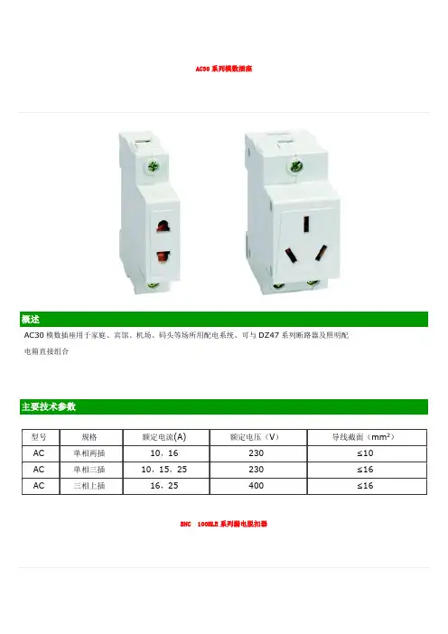
AC30系列模数插座概述AC30模数插座用于家庭、宾馆、机场、码头等场所用配电系统、可与DZ47系列断路器及照明配电箱直接组合主要技术参数型号规格额定电流(A) 额定电压(V)导线截面(mm2)AC 单相两插10,16 230 ≤10 AC 单相三插10,15,25 230 ≤16 AC 三相上插16,25 400 ≤16BNC 100HLE系列漏电脱扣器适用范围BNC 100HLE系列漏电脱扣器主要适用于交流50HZ/60HZ,额定电压为230V/400V及以下,额定电流至63A的线路中,具有漏电触电、过载、短路等保护功能。
还可根据需要增加过呀、欠压保护功能。
主要用于建筑照明和配电系统的保护。
主要技术参数壳架登记额定电流lnm(A)极数(P)额定电压lnm(V)额定短路分断能力而定漏电动作电流l△n(mA)脱扣类型电压(V)分断能力lcuCOS¢100 1+N63、80、10023010KA 0.830C2 503+N 100340030041+N 63、80、100 230 10KA 0.8 30 D2 50 3+N 1003400 3004外形及安装尺寸BNC100H/D系列小型断路器适用范围BNC 100H/D系列小型断路器具有美观小巧、重量轻、性能优良可靠、分段能力较高、脱扣迅速、导轨安装、壳体和部件采用高阻燃及耐冲击塑料、使用寿命长等优点。
主要用于交流50HZ或60HZ单极 230V,二、三、四极400V线路的过载、短路保护,同时也可以在正常情况下不频繁地通断电气装置和照明线路。
主要技术参数断路器的基本参数型号极数(P)额定频率(HZ)壳架等级额定电流(A)额定电压(V)额定电流(A)额定短路分断能力(KA)BNC 100H/D 1、2、3、450、60 100 230/40063、80、10010外形及安装尺寸CE65LE-63(DZ47LE)系列漏电脱扣器主要技术参数CE65LE-63系列漏电断路器主要适用于交流50HZ/60HZ,额定电压为230V/400V及以下,额定电流至63A的线路中,具有漏电触电、过载、短路等保护功能。
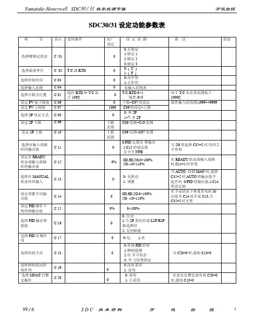
S D C30/31设定功能参数表在C显示时,低于20C的值不显示, 在F显示时,低于68F的值不显示. * * 在–200.0C 不能设定和显示,但在-200.0 C 时可以调节.注 2:在C08中显示这些内容,但当PID 范围采用时(C17=1),可显示出0~7 注3: 当远程功能选择时,PIDr 才显示,PID 范围不可采用(C17=1) 注4: 当采用抗扰动PID 采用时(C19=1)本显示出现。
.1: 参数设定的基本方法如下:(1和 键3秒使仪表进入基本参数设置状态 ( 2 ) 按 和 键来选择希望设定的参数组 ( 3 ) 按 ENT 键使仪表进入设定参数组状态 ( 4 ) 按 或 键来选择希望的参数 ( 5 ) 按 ENT 键使仪表进入参数值设定状态 ( 6 ) 按 或 键来设定希望的参数值 ( 7 ) 按 ENT 键使设定参数值存储于仪表中( 8 ) 按 2 次 DISP 键使仪表恢复到基本设定状态,当只按 1 次 DISP 键时, 仪表进入参数组显示状态.2: 启动 / 停止自整定功能 启动方法:( 1 ) 进入基本显示状态: 按DISP 健此时显示PV 值 显示SP 值 ( 2 ) 进入At (自整定)显示显示 按 MODE 健多次直到At 显示,闪动 再按 ENT 键。
( 3 ) 改变设定值,按 健使0变1,闪动 ( 4 ) 按ENT 键,闪动停止,设定值确定,AT LED 闪动,自整定启动. ( 5 )当自整定完成后,AT 灯熄灭,PID 常数自动写入仪表中.停止方法( 1 ) 进入基本显示状态: 按DISP健此时显示PV值显示SP.MV值( 2 ) 进入At(自整定)显示显示按 MODE 健多次直到At显示,闪动再按 ENT 键。
( 3 ) 。
按健使1变0,( 4 ) 按ENT 键,闪动停止,设定值确定,.( 5 ).按DISP键,恢复基本显示状态3.RUN/READY状态的切换( 例如:从readyd( 1 ) 进入基本显示状态: 按DISP健此时显示PV值显示SP.MV值( 2 ) 进入状态显示显示按 MODE 健2次无显示( 3 ) 显示按或健使显示”run”,( 4 ) 按ENT 键,状态确定,.4.本机SP(LSP) / 远程SP(LSP)的切换。

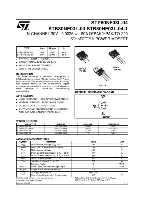
1/11February 2003.STP80NF03L-04STB80NF03L-04 STB80NF03L-04-1N-CHANNEL 30V - 0.0035 Ω - 80A D 2PAK/I 2PAK/TO-220STripFET™ II POWER MOSFETs TYPICAL R DS (on) = 0.0035Ωs EXCEPTIONAL dv/dt CAPABILITY s 100% AVALANCHE TESTED sLOW THRESHOLD DRIVEDESCRIPTIONThis Power MOSFET is the latest development of STMicroelectronis unique "Single Feature Size™" strip-based process. The resulting transistor shows extremely high packing density for low on-resistance, rugged avalanche characteristics and less critical alignment steps therefore a remarkable manufacturing reproducibility.APPLICATIONSs HIGH CURRENT, HIGH SPEED SWITCHING s MOTOR CONTROL, AUDIO AMPLIFIERS s DC-DC & DC-AC CONVERTERSs AUTOMOTIVE ENVIRONMENT (INJECTION, ABS, AIR-BAG, LAMPDRIVERS, Etc.)TYPEV DSS R DS(on)I D STB80NF03L-04/-1STP80NF03L-0430 V 30 V<0.004 Ω<0.004 Ω80 A 80 AOrdering InformationABSOLUTE MAXIMUM RATINGS(Pulse width limited by safe operating area.(**) Current Limited by Package(1) I SD ≤80A, di/dt ≤240A/µs, V DD ≤ 24V, T j ≤ T JMAX (2) Starting T j = 25 o C, I D = 40A, V DD = 20VSALES TYPEMARKING PACKAGE PACKAGINGSTB80NF03L-0480NF03L-04 @D 2PAK TUBE STB80NF03L-04T480NF03L-04 @D 2PAK TAPE & REELSTP80NF03L-0480NF03L-04 @TO-220TUBE STB80NF03L-04-180NF03L-04 @I 2PAKTUBESymbol Parameter Value Unit V DS Drain-source Voltage (V GS = 0)30V V DGRDrain-gate Voltage (R GS = 20 k Ω)30V V GS Gate- source Voltage± 20V I D (**)Drain Current (continuous) at T C = 25°C 80A I D (**)Drain Current (continuous) at T C = 100°C 80A I DM (•)Drain Current (pulsed)320A P tot Total Dissipation at T C = 25°C300W Derating Factor2W/°C dv/dt (1)Peak Diode Recovery voltage slope 2V/ns E AS (2)Single Pulse Avalanche Energy 2.3J T stg Storage Temperature -60 to 175°C T j Max. Operating Junction Temperature 175°CSTB80NF03L-04/-1/STP80NF03L-042/11THERMAL DATAELECTRICAL CHARACTERISTICS (T case = 25 °C unless otherwise specified)OFFON (*)DYNAMICRthj-case Rthj-ambT lThermal Resistance Junction-case Thermal Resistance Junction-ambientMaximum Lead Temperature For Soldering PurposeMax Max Typ0.562.5300°C/W °C/W °CSymbol ParameterTest ConditionsMin.Typ.Max.Unit V (BR)DSS Drain-sourceBreakdown Voltage I D = 250 µAV GS = 030V I DSSZero Gate VoltageDrain Current (V GS = 0)V DS = Max RatingV DS = Max Rating T C = 125°C 110µA µA I GSSGate-body Leakage Current (V DS = 0)V GS = ± 20 V±100nASymbol ParameterTest ConditionsMin.Typ.Max.Unit V GS(th)Gate Threshold Voltage V DS = V GS I D = 250 µA 1V R DS(on)Static Drain-source On ResistanceV GS = 10 V I D = 40 A V GS = 4.5 VI D = 40 A0.00350.0040.0040.0055ΩΩSymbol ParameterTest ConditionsMin.Typ.Max.Unit g fs (*)Forward Transconductance V DS = 15 VI D =15 A50S C iss C oss C rssInput Capacitance Output Capacitance Reverse Transfer CapacitanceV DS = 25V, f = 1 MHz, V GS = 055001670290pF pF pFSTB80NF03L-04/-1/STP80NF03L-04SWITCHING ONSWITCHING OFFSOURCE DRAIN DIODE(*)Pulsed: Pulse duration = 300 µs, duty cycle 1.5 %.(•)Pulse width limited by safe operating area.Symbol ParameterTest ConditionsMin.Typ.Max.Unit t d(on)t r Turn-on Delay Time Rise TimeV DD = 15 VI D = 40 A R G =4.7 Ω V GS = 4.5 V (Resistive Load, Figure 3)30270ns ns Q g Q gs Q gdTotal Gate Charge Gate-Source Charge Gate-Drain ChargeV DD =24V I D =80 A V GS =4.5V852340110nC nC nCSymbol ParameterTest ConditionsMin.Typ.Max.Unit t d(off)t f Turn-off Delay Time Fall TimeV DD = 15 VI D = 40 A R G =4.7Ω, V GS = 4.5 V (Resistive Load, Figure 3)11095ns ns t r(Voff)t f t cOff-Voltage Rise Time Fall TimeCross-over TimeV clamp = 24 VI D = 80 A R G =4.7Ω V GS = 4.5 V (Inductive Load, Figure 5)12575125ns ns nsSymbol ParameterTest ConditionsMin.Typ.Max.Unit I SD I SDM (•)Source-drain CurrentSource-drain Current (pulsed)80320A A V SD (*)Forward On Voltage I SD = 80 AV GS = 01.5V t rr Q rr I RRMReverse Recovery Time Reverse Recovery Charge Reverse Recovery CurrentI SD = 80 Adi/dt = 100A/µs V DD = 20 V T j = 150°C (see test circuit, Figure 5)750.154ns µC AELECTRICAL CHARACTERISTICS (continued)STB80NF03L-04/-1/STP80NF03L-04STB80NF03L-04/-1/STP80NF03L-04STB80NF03L-04/-1/STP80NF03L-046/11Fig. 3: Switching Times Test Circuits For ResistiveFig. 5: Test Circuit For Inductive Load Switching7/11STB80NF03L-04/-1/STP80NF03L-04DIM.mm.inch.MIN.TYP. MAX.MIN.TYP. TYP .A 4.4 4.60.1730.181A1 2.49 2.690.0980.106A20.030.230.0010.009B 0.70.930.0280.037B2 1.14 1.70.0450.067C 0.450.60.0180.024C2 1.21 1.360.0480.054D 8.959.350.3520.368D180.315E 1010.40.3940.409E18.50.334G 4.88 5.280.1920.208L 1515.850.5910.624L2 1.27 1.40.0500.055L3 1.4 1.750.0550.069M 2.43.20.0940.126R 0.40.015V20°8°0°8°D 2PAK MECHANICAL DATASTB80NF03L-04/-1/STP80NF03L-0410/11DIM.mm inchMIN.MAX.MIN.MAX.A010.510.70.4130.421B015.715.90.6180.626D 1.5 1.60.0590.063D1 1.59 1.610.0620.063E 1.65 1.850.0650.073F11.411.60.4490.456K0 4.8 5.00.1890.197P0 3.9 4.10.1530.161P111.912.10.4680.476P2 1.9 2.100750.082R50 1.574T0.250.35.0.00980.0137W23.724.30.9330.956DIM.mm inchMIN.MAX.MIN.MAX.A33012.992B 1.50.059C12.813.20.5040.520D20.20.795G24.426.40.960 1.039N100 3.937T30.4 1.197BASE QTY BULK QTY10001000REEL MECHANICAL DATA* on sales typeTUBE SHIPMENT (no suffix)* TAPE AND REEL SHIPMENT (suffix ”T4”)*D2PAK FOOTPRINTTAPE MECHANICAL DATA元器件交易网STB80NF03L-04/-1/STP80NF03L-04 Information furnished is believed to be accurate and reliable. However, STMicroelectronics assumes no responsibility for the consequencesof use of such information nor for any infringement of patents or other rights of third parties which may result from its use. No license is grantedby implication or otherwise under any patent or patent rights of STMicroelectronics. Specifications mentioned in this publication are subjectto change without notice. This publication supersedes and replaces all information previously supplied. STMicroelectronics products are notauthorized for use as critical components in life support devices or systems without express written approval of STMicroelectronics.The ST logo is registered trademark of STMicroelectronics® 2002 STMicroelectronics - All Rights ReservedAll other names are the property of their respective owners.STMicroelectronics GROUP OF COMPANIESAustralia - Brazil - Canada - China - Finland - France - Germany - Hong Kong - India - Israel - Italy - Japan - Malaysia - Malta - Morocco -Singapore - Spain - Sweden - Switzerland - United Kingdom - United States.11/11。
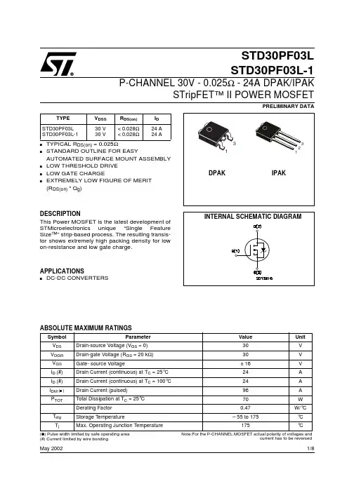
1/8PRELIMINARY DATAMay 2002STD30PF03L STD30PF03L-1P-CHANNEL 30V - 0.025Ω - 24A DPAK/IPAKSTripFET™ II POWER MOSFETNote:For the P-CHANNEL MOSFET actual polarity of voltages andcurrent has to be reverseds TYPICAL R DS(on) = 0.025ΩsSTANDARD OUTLINE FOR EASYAUTOMATED SURFACE MOUNT ASSEMBLY s LOW THRESHOLD DRIVE s LOW GATE CHARGEsEXTREMELY LOW FIGURE OF MERIT (R DS(on) * Q g )DESCRIPTIONThis Power MOSFET is the latest development of STMicroelectronics unique “Single Feature Size™” strip-based process. The resulting transis-tor shows extremely high packing density for low on-resistance and low gate charge.APPLICATIONSs DC-DC CONVERTERSABSOLUTE MAXIMUM RATINGS(q ) Pulse width limited by safe operating area (#) Current limited by wire bondingTYPE V DSS R DS(on)I D STD30PF03L STD30PF03L-130 V 30 V< 0.028Ω< 0.028Ω24 A 24 ASymbol ParameterValue Unit V DSDrain-source Voltage (V GS = 0)30V V DGR Drain-gate Voltage (R GS = 20 k Ω)30V V GSGate- source Voltage± 16V I D (#)Drain Current (continuous) at T C = 25°C 24A I D (#)Drain Current (continuous) at T C = 100°C 24A I DM (l )Drain Current (pulsed)96A P TOT Total Dissipation at T C = 25°C 70W Derating Factor 0.47W/°C T stg Storage Temperature– 55 to 175°C T jMax. Operating Junction Temperature175°CSTD30PF03L - STD30PF03L-12/8THERMAL DATAAVALANCHE CHARACTERISTICSELECTRICAL CHARACTERISTICS (TCASE = 25 °C UNLESS OTHERWISE SPECIFIED)OFFON (1)DYNAMICRthj-case Thermal Resistance Junction-case Max 2.14°C/W Rthj-ambThermal Resistance Junction-ambient Max 100°C/W T jMaximum Operating Junction Temperature275°CSymbol ParameterMax ValueUnit I AR Avalanche Current, Repetitive or Not-Repetitive (pulse width limited by T j max)24A E ASSingle Pulse Avalanche Energy(starting T j = 25 °C, I D = I AR , V DD = 25 V)350mJSymbol ParameterTest ConditionsMin.Typ.Max.Unit V (BR)DSS Drain-sourceBreakdown Voltage I D = 250 µA, V GS = 030V I DSS Zero Gate VoltageDrain Current (V GS = 0)V DS = Max Rating1µA V DS = Max Rating, T C = 125 °C 10µA I GSSGate-body Leakage Current (V DS = 0)V GS = ± 16 V±100nASymbol ParameterTest ConditionsMin.Typ.Max.Unit V GS(th)Gate Threshold Voltage V DS = V GS , I D = 250µA 1V R DS(on)Static Drain-source On ResistanceV GS = 10 V, I D = 12 A 00250.028ΩV GS = 5 V, I D = 12 A0.0320.040ΩSymbol ParameterTest ConditionsMin.Typ.Max.Unit g fs (1)Forward Transconductance V DS = 15 V , I D = 12 A23S C iss Input Capacitance V DS = 25V, f = 1 MHz, V GS = 01670pF C oss Output Capacitance 345pF C rssReverse Transfer Capacitance120pF3/8STD30PF03L - STD30PF03L-1ELECTRICAL CHARACTERISTICS (CONTINUED)SWITCHING ONSWITCHING OFFSOURCE DRAIN DIODENote: 1.Pulsed: Pulse duration = 300 µs, duty cycle 1.5 %.2.Pulse width limited by safe operating area.Symbol ParameterTest ConditionsMin.Typ.Max.Unit t d(on)Turn-on Delay Time V DD = 24 V, I D = 24 A R G =4.7Ω V GS = 4.5V (see test circuit, Figure 3)64ns t r Rise Time122ns Q g Q gs Q gdTotal Gate Charge Gate-Source Charge Gate-Drain ChargeV DD = 15 V, I D = 24 A,V GS = 5 V18.55.51125nC nC nCSymbol ParameterTest ConditionsMin.Typ.Max.Unit t d(off)t fTurn-off-Delay Time Fall TimeV DD = 24 V, I D = 24 A,R G =4.7Ω, V GS = 4.5V (see test circuit, Figure 3)3626ns nsSymbol ParameterTest ConditionsMin.Typ.Max.Unit I SD Source-drain Current 24A I SDM (2)Source-drain Current (pulsed)96A V SD (1)Forward On Voltage I SD = 24 A, V GS = 0 2.3V t rr Q rr I RRMReverse Recovery Time Reverse Recovery Charge Reverse Recovery CurrentI SD = 24 A, di/dt = 100 A/µs,V DD = 24 V, T j = 150 °C (see test circuit, Figure 5)40522.6ns µC ASTD30PF03L - STD30PF03L-14/8Fig. 5: Test Circuit For Inductive Load Switching And Diode Recovery TimesFig. 4: Gate Charge test CircuitFig. 2: Unclamped Inductive WaveformFig. 1:Unclamped Inductive Load Test CircuitFig. 3: Switching Times Test Circuit ForResistive LoadSTD30PF03L - STD30PF03L-15/8STD30PF03L - STD30PF03L-16/87/8STD30PF03L - STD30PF03L-1TAPE AND REEL SHIPMENT (suffix ”T4”)*TUBE SHIPMENT (no suffix)*DPAK FOOTPRINT * on sales typeDIM.mm inch MIN.MAX.MIN.MAX.A 33012.992B 1.50.059C 12.813.20.5040.520D 20.20.795G 16.418.40.6450.724N 501.968T22.40.881BASE QTY BULK QTY 25002500REEL MECHANICAL DATADIM.mm inch MIN.MAX.MIN.MAX.A0 6.870.2670.275B010.410.60.4090.417B112.10.476D 1.5 1.60.0590.063D1 1.50.059E 1.65 1.850.0650.073F 7.47.60.2910.299K0 2.55 2.750.1000.108P0 3.9 4.10.1530.161P17.98.10.3110.319P2 1.9 2.10.0750.082R 40 1.574W15.716.30.6180.641TAPE MECHANICAL DATAAll dimensions are in millimetersAll dimensions are in millimetersSTD30PF03L - STD30PF03L-18/8Information furnished is believed to be accurate and reliable. However, STMicroelectronics assumes no responsibility for the consequences of use of such information nor for any infringement of patents or other rights of third parties which may result from its use. No license is granted by implication or otherwise under any patent or patent rights of STMicroelectronics. Specifications mentioned in this publication are subject to change without notice. This publication supersedes and replaces all information previously supplied. STMicroelectronics products are not authorized for use as critical components in life support devices or systems without express written approval of STMicroelectronics.© The ST logo is a registered trademark of STMicroelectronics© 2002 STMicroelectronics - Printed in Italy - All Rights ReservedSTMicroelectronics GROUP OF COMPANIESAustralia - Brazil - Canada - China - Finland - France - Germany - Hong Kong - India - Israel - Italy - Japan - Malaysia - Malta - Morocco Singapore - Spain - Sweden - Switzerland - United Kingdom - United States.© 。
" ! " ! " ! "! " # $% # & # # ' ( # ) **µ+ , - . . Ω, / , - 0 **-0 . 1. / " ! " ** 2 % (%( 3 4 % 5 #! "E+ E @ + + - * + 5 - '.* µ()* +∆E+ $ ∆ E @ +5 - '.* µ( , '.9 * *) +$9 5 F < + + - )* + + - * + 0µ(+ - D; + - 0.*9 0*µ(5 < E 1 @ + - '* + + - * + 0** (5< E 1 @ , !+ - '* + + - * +0**(+ < + + - + 5 - '.* µ(0 * ' .+, ,+ - 0* + 5 - 0) (+ - . + 5 -0) (* *'6* *&.* *&.* *D.Ω+ - '. + 5 - 0) ('D5 + - '. + + - * + - 0 * G#;**0*D*'6*&.*, !.*).+ - &* + 5 - 0) ( , - '. Ω0.D* , '0*D&* )*0&* 00*'&* H < + - D; + 5 - &' ( + - . +0.'* H < & . H<; .5 7 &'(5 7 :0';(+ + + - * + 5 - &' ( 0 .+ , ! , ! + - * + 5 - &' (5 $ - 0** ($µ)* H, ! , !?*TRADEMARKSThe following are registered and unregistered trademarks Fairchild Semiconductor owns or is authorized to use and is not intended to be an exhaustive list of all such trademarks.LIFE SUPPORT POLICYFAIRCHILD’S PRODUCTS ARE NOT AUTHORIZED FOR USE AS CRITICAL COMPONENTS IN LIFE SUPPORTDEVICES OR SYSTEMS WITHOUT THE EXPRESS WRITTEN APPROVAL OF FAIRCHILD SEMICONDUCTOR CORPORATION.As used herein:1. Life support devices or systems are devices or systems which, (a) are intended for surgical implant intothe body, or (b) support or sustain life, or (c) whosefailure to perform when properly used in accordancewith instructions for use provided in the labeling, can be reasonably expected to result in significant injury to the user.2. A critical component is any component of a lifesupport device or system whose failure to perform can be reasonably expected to cause the failure of the life support device or system, or to affect its safety or effectiveness.PRODUCT STATUS DEFINITIONS Definition of Terms Datasheet Identification Product Status DefinitionAdvance InformationPreliminary No Identification Needed Obsolete This datasheet contains the design specifications for product development. Specifications may change in any manner without notice.This datasheet contains preliminary data, andsupplementary data will be published at a later date.Fairchild Semiconductor reserves the right to make changes at any time without notice in order to improve design.This datasheet contains final specifications. Fairchild Semiconductor reserves the right to make changes at any time without notice in order to improve design.This datasheet contains specifications on a product that has been discontinued by Fairchild semiconductor.The datasheet is printed for reference information only.Formative or In DesignFirst ProductionFull ProductionNot In ProductionDISCLAIMERFAIRCHILD SEMICONDUCTOR RESERVES THE RIGHT TO MAKE CHANGES WITHOUT FURTHER NOTICE TO ANY PRODUCTS HEREIN TO IMPROVE RELIABILITY , FUNCTION OR DESIGN. FAIRCHILD DOES NOT ASSUME ANY LIABILITY ARISING OUT OF THE APPLICATION OR USE OF ANY PRODUCT OR CIRCUIT DESCRIBED HEREIN; NEITHER DOES IT CONVEY ANY LICENSE UNDER ITS PATENT RIGHTS, NOR THE RIGHTS OF OTHERS.QFET™QS™QT Optoelectronics™Quiet Series™SuperSOT™-3SuperSOT™-6SuperSOT™-8SyncFET™TinyLogic™UHC™FASTr™GlobalOptoisolator™GTO™HiSeC™ISOPLANAR™MICROWIRE™OPTOLOGIC™OPTOPLANAR™POP™PowerTrench ®Rev. F1ACEx™Bottomless™CoolFET™CROSSVOLT™DOME™E 2CMOS TM EnSigna TM FACT™FACT Quiet Series™FAST ®VCX™元器件交易网。
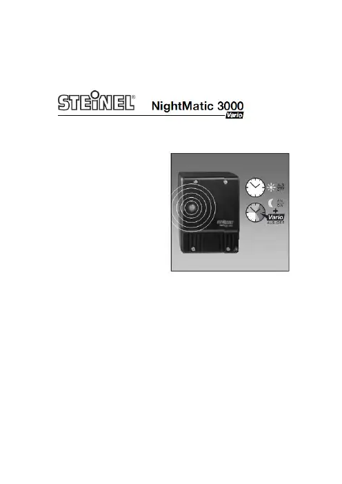
尊敬的顾客:感谢您购买了新的施特朗感应器,并感谢您对我们的信任。
您选择了生产、测试以及包装过程都经过严格监控的高质量产品。
安装前请仔细阅读该安装说明,因为只有正确的操作才能保证它能可靠方便地为您服务。
希望您的新感应器带给您无尽的乐趣。
施特朗(中国)管理机构原理光敏控制感应器可以测量周围的光敏度并在黑夜降临时自动打开连接的灯具,而在清晨时灯则自动熄灭。
若设置了夜间经济模式,则光敏控制器自动在黑夜时分打开照明,在午夜根据设定的时间关闭照明;设定的时间过后,天还没亮的话,照明重新打开。
安装墙壁安装注意:连接230伏的电源会有触电的危险!因此必须先关掉电源并用电笔测试电压。
光敏控制器的安装涉及到用电,因此必须严格按照规定来进行。
请注意光敏控制器必须接上10安的电路保护器,主电源线的截面直径不能大于10毫米,要确保N3000不受所连接的灯具的灯光影响(如不要让灯光直接照在感应器上)。
用螺丝刀按逆时针方向把四颗螺丝松开并取下盖子,把基座按在墙面并在墙上需要打孔的地方做下标记,注意电线的位置。
在墙上打孔并插入螺丝塞,不管什么情况电源线都要从下面插入。
固定基座之前先把底部的排水孔刺穿。
连接:端口如下标志:L =火线(黑色或棕色)N =零线(蓝色)PE=接地线(绿色或黄色)如果你不太确定请用电笔测试。
把火线和零线接到相应的端口,把灯具连接到第二个火线与零线的接口,把绿色或黄色的接地线连接到接地的端口。
注意:如果线路连接相反会造成短路,这种情况下你需要再次检查连接的线并纠正。
调试/功能这要连接完成,用户的照明设备接通电源8秒后,光敏测量设置随后启动。
光敏设置:光敏的出厂设置为1lux,可通过以下方法进行设置:在您认为需要启动照明的光线条件下,用圆珠笔或小型的物体按下按钮(参照图识)直至LED灯闪烁,然后松开。
感应器会存储当时的环境亮度值约需10秒(如有需要请关掉连接的照明),下次会根据所设定的光敏值感应亮灯。
(由于光敏值的限制,光敏设置不能在白天环境下进行。
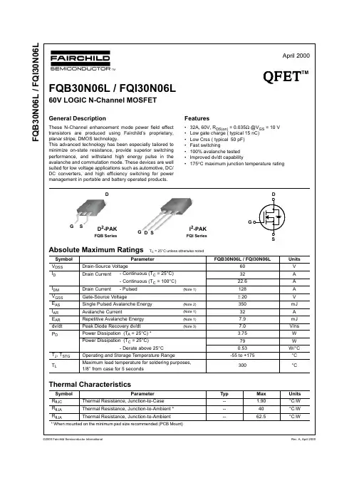
ConformityDirective MID 2014/32/EC, 0120/SGS0306Norm EN50470-1/3PurposeLE-03MW is an electronic, compliant with the MID Directive, 2-way electricity meter for three-phase electricity, designed for measu-rement in a direct system.The built-in real-time clock allows energy consumption to be mea-sured with different tariff zones.The device is equipped with communication interfaces: RS-485 with Modbus RTU protocol and optical port compliant with EN62056 (IEC1107) standard for remote reading and configuration of the meter.Manual and programming instructionsFull technical documentation of the device for download fromthewebsite:.pl3-phase, 2-way energy meter;* direct measurement up to 80 A;* energy measurement in 4 tariff zones;* built-in real time clock with battery backup to switch tariff zones;* registration of total and divided into consumption tariffs:– total active and reactive energy;– active and reactive energy divided into individual quadrants;* 8 time schedules dividing the day into tariff zones;* it can settle energy according to schedules specific for businessdays and weekends;* it can divide year into 8 time intervals; in each interval the energy(for weekdays) can be settled according to a different schedule;* indication of network parameters (voltages, currents, active po-wer, reactive power, apparent power, power factor, frequency);* calculation of power demand for individual tariffs;* an additional, resettable energy consumption meter;* compliance with MID;* RS-485 port, Modbus RTU protocol;* optical communication port compliant with EN62056 (IEC1107)standard;* 2× SO pulse outputs with a programmable number of pulses perkWh / kvarh.* multifunction LCD display.Functions*Measured valuesCApparent powerPower factoronsumed and suppliedactive energyI nductive and capacitivereactive energyC onsumed and suppliedactive powerI nductive and capacitivereactive powerAE+/AE- [kWh]RE+/RE- [kvarh]U1, U2, U3 [V]I1, I2, I3 [A]Frequency F [Hz]P [W]Q [var]S [VA]cosϕPhase voltagesPhase currentsMeter numberThe meter is marked with individual serial number allowing itsunambiguous identification.The marking is laser engraved and cannot be removed.SealingThe meter has sealable input and output terminal covers to pre-vent any attempts to bypass the meter.- 1 -- 2 -- 3 -- 4 -sealing spotWiring diagram Technical data ontinued from the previous pag insulation protection class self-extinguishing materialService programOn the .pl website (on the subpage of the LE-03MW meter) a program is available for PCs with Windows that allows checking the readings of the meter and making all its settings.(c )reading indication 2×LED working temperature -25÷55°Cterminal 25 mm² screw terminals dimensions76×100×65 mm (4,5 modules DIN)mountingon the TH-35 mm rail protection levelIP51class IIhousingUI94 V-0 CE declarationA copy of the CE declaration is available for download from the website: .pl from the product subpage.- 5 -- 6 -D190118Technical datareference voltage3×230/400 V minimum current/base current 0.25/5 A maximum current80 A minimum detection current 0.04 Avoltage measuring current L-N 100÷289 V AC L-L173÷500 V AC rated frequency50 Hz measurement accuracy B classinstalation 3-phase, 4-wire overloading 30×lmax/10 msinsulation4 kV/1 min.; 6 kV/1 μs own meter consumption <10 VA; <2 W measured values8 digitsindication range of the meter number of pulse outputs type of pulse outputs pulse constant for output 1pulse constant for output continued on the next page pulse outputs2OC (open collector)maximum voltage 30 V DC maximum current27 mA1; 10; 100; 1000 pulse/kWh 21000 pulse/kvarcommunication portRS-485communication protocol Modbus RTUtransmission speed 1200, 2400, 4800, 9600 bps parity EVEN parity bits2()20, 21–RS-485 (A, B)23, 24–pulse outputIN。
用户操作手册请您在使用前仔细阅读本操作手册,以获得更好的使用体验。
目录主要特点 (3)LS30包装盒内部件 (4)注意事项 (5)免责声明 (5)商标声明 (5)本说明书中特定符号作用 (6)1准备 71 各部分介绍 (8)2 界面 (10)3 使用电池 (11)安装电池 (11)取出电池 (12)4 锁定按键(HOLD) (13)5 开关机.............................................146 设置时间日期 (15)2录音 161 录音基本操作 (17)2 录音模式 (19)课堂模式 (19)口袋模式 (19)手动录音模式 (20)设置录音模式 (21)3 手动调节输入增益(LEVEL) (22)4 AGC(自动调节增益) (23)5 声控录音(VOR) (25)6 低切降噪(LOW CUT) (27)7 外置输入设备 (28)3播放 291 播放基本操作 (30)2 变速播放(SPEED) (32)3 A-B重复播放 (34)4 循环模式 (35)5 使用扬声器或耳机 (36)6 删除文件 (37)4菜单功能 381 菜单操作方法 (39)2 选项介绍 (40)5传输数据 471 系统及硬件要求..............................482 文件夹结构 (49)3 传输文件 (50)6故障排除 531 系统提示 (54)2 常见问题 (58)7其他信息 611 规格 (62)2 安全说明 (64)主要特点一键录音:长按REC键直接 进入课堂模式移植多项专业采访机技术环境音抑制系统变速复听不变调广播级专业降噪语音质量提升140小时录音 / 声控录音/ 无损PCM / A-B复读衣服口袋和包内清晰录音LS30包装盒内部件• LS30包装盒内包括如下标准部件各一件,购买产品时,请对照此装箱清单认真核实主机、 标准附件、选配附件是否齐全。
官方微信官方网站目 录SDAC6000(u)量热仪SDACM4000量热仪SDACM3100量热仪SDC712量热仪SDC715量热仪01-05热值分析系列020*********-11元素分析系列SDCHN536碳氢氮元素分析仪SDCH536红外碳氢仪SDH536红外测氢仪SDS350红外定硫仪SDS820自动定硫仪SDS720自动定硫仪SDS-V 定硫仪SDFCl3000自动氟氯分析仪SDFCl1000(a)氟氯分析仪070707080909101111SDTGA8000(a)工业分析仪SDTGA6000工业分析仪SDTGA6000A 工业分析仪SDTGA6000V 工业分析仪SDTGA5000a 工业分析仪SDTGA520(a)水分测试仪SDTGA500光波水分测试仪SDIMF200智能马弗炉SDMF300马弗炉SDIDB413智能干燥箱SDDH315通氮鼓风干燥箱SDDH323鼓风干燥箱SDDH313鼓风干燥箱SDDH306鼓风干燥箱12-22成分分析系列1314151516171819202121222222SDAF105(a /b )灰熔融性测试仪SDAF4000灰熔融性测试仪SDHG60a 哈氏可磨性指数测定仪23-26物理特性分析系列242526S DUC3150(D )联合制样机S DHD150t 锤式破碎缩分机S DHC锤式破碎机S DJC颚式破碎机S DRC对辊破碎机S DHCW400×260湿煤破碎机S DPP制样粉碎机S DMD16自动机械缩分器S DNS300环保振筛机S DNS200a标准振筛机S DRD二分器采制样辅助工具30-38样品制备系列313232333334343535353637-38激光盘料仪系列SDLM200便携式激光盘料仪SDLM1250固定式激光盘料仪39-41404142-43公司简介44发展历程45运维服务2829S DVD25风透 式快速除湿干燥系统S DVD3mm 风透 干燥机27-29风透 式低温快速除湿干燥系列热值分析系列适用范围符合标准GB/T213-2008GB/T384-1981 GB/T30727-2014ASTM D5865-2007ISO 1928-2009 JC/T1005-2006《煤的发热量测定方法》《石油产品热值测定法》《固体生物质燃料发热量测定方法》《煤与焦炭总热值的标准试验方法》《固体矿物燃料-氧弹式量热计测定总值并计算净热值》《水泥黑生料发热量测定方法》三德科技是中国第一台自动量热仪(1996年)的发明者,先后自主研发出6代量热仪,缔造了2个“国家重点新产品”。
STD30NF03LN -CHANNEL 30V -0.020Ω-30A DPAKSTripFET ™POWER MOSFETs TYPICAL R DS(on)=0.020Ωs LOW THRESHOLD DRIVEsADD SUFFIX ”T4”FOR ORDERING IN TAPE &REELDESCRIPTIONThis Power MOSFET is the latest development of STMicroelectronics unique ”Single Feature Size ™”strip-based process.The resulting transistor shows extremely high packing density for low on-resistance,rugged avalanche characteristics and less critical alignment steps therefore a remarkable manufacturing reproducibility.APPLICATIONSs HIGH CURRENT,HIGH SPEED SWITCHING s SOLENOID AND RELAY DRIVERSs MOTOR CONTROL,AUDIO AMPLIFIERS s DC-DC &DC-AC CONVERTERS®INTERNAL SCHEMATIC DIAGRAMOctober 199913DPAK TO-252(Suffix ”T4”)ABSOLUTE MAXIMUM RATINGSSymbol ParameterValue Unit V DS Drain-source Voltage (V GS =0)30V V DGR Drain-gate Voltage (R GS =20k Ω)30V V GS Gate-source Voltage±20V I D (•)Drain Current (continuous)at T c =25o C 30A I D Drain Current (continuous)at T c =100o C 19A I DM (••)Drain Current (pulsed)120A P tot Total Dissipation at T c =25oC 40W Derating Factor0.27W/o C E AS (1)Single Pulse Avalanche Energy 100m/JT st g Storage Temperature-65to 175o C T jMax.Operating Junction Temperature175oC(••)Pulse width limited by safe operating area (1) starting T j =25oC,I D =15A ,V DD =15V(•)Current limited by the packageTYPE V DSS R DS(o n)I D STD30NF03L30V<0.025Ω30A1/8THERMAL DATAR th j-pc b R thj-amb R t hj-s inkT l Thermal Resistance Junction-PC Board MaxThermal Resistance Junction-ambient MaxThermal Resistance Case-sink TypMaximum Lead Temperature For Soldering Purpose3.751001.5275o C/Wo C/Wo C/Wo CELECTRICAL CHARACTERISTICS(T case=25o C unless otherwise specified)OFFSymbol Parameter Test Conditions Min.Typ.Max.Unit V(BR)DSS Drain-sourceBreakdown VoltageI D=250µA V GS=030VI DSS Zero Gate VoltageDrain Current(V GS=0)V DS=Max RatingV DS=Max Rating T c=125o C110µAµAI GSS Gate-body LeakageCurrent(V DS=0)V GS=±20V±100nA ON(∗)Symbol Parameter Test Conditions Min.Typ.Max.Unit V GS(th)Gate Threshold Voltage V DS=V GS I D=250µA1 1.7 2.5VR DS(on)Static Drain-source OnResistance V GS=10V I D=15AV GS=4.5V I D=15A0.0200.0280.0250.035ΩΩI D(o n)On State Drain Current V DS>I D(o n)x R DS(on)ma xV GS=10V30A DYNAMICSymbol Parameter Test Conditions Min.Typ.Max.Unitg f s(∗)ForwardTransconductanceV DS>I D(o n)x R DS(on)ma x I D=15A13SC iss C os s C rss Input CapacitanceOutput CapacitanceReverse TransferCapacitanceV DS=25V f=1MHz V GS=0V83023092pFpFpFSTD30NF03L 2/8ELECTRICAL CHARACTERISTICS(continued)SWITCHING ONSymbol Parameter Test Conditions Min.Typ.Max.Unitt d(on) t r Turn-on Delay TimeRise TimeV DD=15V I D=20AR G=4.7 ΩV GS=4.5V(Resistive Load,see fig.3)35205nsnsQ g Q gs Q gd Total Gate ChargeGate-Source ChargeGate-Drain ChargeV DD=24V I D=30A V GS=5V1878nCnCnCSWITCHING OFFSymbol Parameter Test Conditions Min.Typ.Max.Unitt d(of f) t f Turn-off Delay TimeFall TimeV DD=15V I D=20AR G=4.7 ΩV GS=4.5V(Resistive Load,see fig.3)90240nsnsSOURCE DRAIN DIODESymbol Parameter Test Conditions Min.Typ.Max.UnitI SD I SDM(•)Source-drain CurrentSource-drain Current(pulsed)30120AAV SD(∗)Forward On Voltage I SD=30A V GS=0 1.5Vt rr Q rr I RRM Reverse RecoveryTimeReverse RecoveryChargeReverse RecoveryCurrentI SD=40A di/dt=100A/µsV DD=15V T j=150o C(see test circuit,fig.5)65722nsnCA(∗)Pulsed:Pulse duration=300µs,duty cycle1.5%(•)Pulse width limited by safe operating areaSafe Operating Area Thermal ImpedanceSTD30NF03L3/8Output Characteristics TransconductanceGate Charge vs Gate-source Voltage Transfer CharacteristicsStatic Drain-source On Resistance Capacitance VariationsSTD30NF03L 4/8Normalized Gate Threshold Voltage vs TemperatureSource-drain Diode Forward Characteristics Normalized On Resistance vs TemperatureSTD30NF03L5/8Fig.1:Unclamped Inductive Load Test Circuit Fig.3:Switching Times Test Circuits For Resistive Load Fig.2:Unclamped Inductive Waveform Fig.4:Gate Charge test CircuitFig.5:Test Circuit For Inductive Load Switching And Diode Recovery TimesSTD30NF03L6/8DIM.mminch MIN.TYP.MAX.MIN.TYP.MAX.A 2.2 2.40.0860.094A10.9 1.10.0350.043A20.030.230.0010.009B 0.640.90.0250.035B2 5.2 5.40.2040.212C 0.450.60.0170.023C20.480.60.0190.023D 6 6.20.2360.244E 6.4 6.60.2520.260G 4.4 4.60.1730.181H 9.3510.10.3680.397L20.80.031L40.610.0230.039==DL2L413==BE==B 2G2AC 2CHA 1DETAIL ”A”A 2DETAIL ”A”TO-252(DPAK)MECHANICAL DATA0068772-BSTD30NF03L7/8Information furnished is believed to be accurate and reliable.However,STMicroelect r onics assumes no responsibility for the consequences of use of such information nor for any infringement of patents or other rights of third part i es which may result from its use.No license is granted by implication or otherwise under any patent or patent rights of STMicroelectro nics.Specification mentioned in this publication are subject to change without notice.This publication supersedes and replaces all informat i on previously supplied.STMicroelectronics products are not authorized for use as critical components in life support devices or systems with out express written approval of STMicroelectronics.The ST logo is a trademark of STMicroelectronics©1999STMicroelectronics –Printed in Italy –All Rights ReservedSTMicroelectronics GROUP OF COMPANIESAustralia -Brazil -China -Finland -France -Germany -Hong Kong -India -Italy -Japa n -Malaysia -Malta -Morocco -Singapore -Spain -Sweden -Switzerland -United Kingdom -U.S.A..STD30NF03L8/8。