LT-6
- 格式:doc
- 大小:31.00 KB
- 文档页数:1


123LT6202/LT6203/LT62044620234faELECTRICAL CHARACTERISTICST A = 25°C, V S =5V, 0V; V S = 3V, 0V; V CM = V OUT = half supply,unless otherwise noted.SYMBOL PARAMETER CONDITIONS MINTYP MAXUNITSC IN Input Capacitance Common Mode 1.8pF Differential Mode1.5pF A VOLLarge Signal GainV S = 5V, V O = 0.5V to 4.5V, R L = 1k to V S /24070V/mV V S = 5V, V O = 1V to 4V, R L = 100 to V S /28.014V/mV V S = 3V, V O = 0.5V to 2.5V, R L = 1k to V S /21740V/mV CMRR Common Mode Rejection RatioV S = 5V, V CM = V – to V +6083dB V S = 5V, V CM = 1.5V to 3.5V 80100dB V S = 3V, V CM = V – to V +5680dB CMRR Match (Channel-to-Channel) (Note 6)V S = 5V, V CM = 1.5V to 3.5V 85120dB PSRRPower Supply Rejection RatioV S = 2.5V to 10V, V CM = 0V 6074dB PSRR Match (Channel-to-Channel) (Note 6)V S = 2.5V to 10V, V CM = 0V 70100dB Minimum Supply Voltage (Note 7)2.5V V OLOutput Voltage Swing LOW Saturation No Load 550mV (Note 8)I SINK = 5mA85190mV V S = 5V, I SINK = 20mA 240460mV V S = 3V, I SINK = 15mA 185350mV V OHOutput Voltage Swing HIGH Saturation No Load2575mV (Note 8)I SOURCE = 5mA90210mV V S = 5V, I SOURCE = 20mA 325600mV V S = 3V, I SOURCE = 15mA 225410mV I SC Short-Circuit Current V S = 5V ±30±45mA V S = 3V ±25±40mA I S Supply Current per Amp V S = 5V 2.5 3.0mA V S = 3V2.3 2.85mA GBW Gain Bandwidth Product Frequency = 1MHz, V S = 5V 90MHz SR Slew RateV S = 5V, A V = –1, R L = 1k, V O = 4V 1724V/µs FPBW Full Power Bandwidth (Note 10)V S = 5V, V OUT = 3V P-P1.82.5MHz t SSettling Time0.1%, V S = 5V, V STEP = 2V, A V = –1, R L = 1k85nsThe q denotes the specifications which apply over 0°C < T A < 70°C temperature range. V S = 5V, 0V; V S = 3V, 0V;V CM = V OUT = half supply, unless otherwise noted.SYMBOL PARAMETER CONDITIONSMIN TYP MAX UNITS V OSInput Offset VoltageV S = 5V, 0V, V CM = Half Supply LT6203, LT6204, LT6202S8q 0.20.7mV LT6202 SOT-23q 0.20.9mV V S = 3V, 0V, V CM = Half Supply LT6203, LT6204, LT6202S8q 0.6 1.7mV LT6202 SOT-23q 0.6 1.9mV V S = 5V, 0V, V CM = V + to V –LT6203, LT6204, LT6202S8q 0.7 2.5mV LT6202 SOT-23q 0.7 2.7mV V S = 3V, 0V, V CM = V + to V –LT6203, LT6204, LT6202S8q 1.2 4.0mV LT6202 SOT-23q 1.2 4.2mV V OS TCInput Offset Voltage Drift (Note 9)V CM = Half Supply q 3.09.0µV/°C Input Offset Voltage Match V CM = Half Supply q 0.150.9mV (Channel-to-Channel) (Note 6)V CM = V – to V +q0.52.3mVLT6202/LT6203/LT62045620234faSYMBOL PARAMETER CONDITIONS MIN TYP MAX UNITS I BInput Bias CurrentV CM = Half Supply q –7.0–1.3µA V CM = V +q 1.3 2.5µA V CM = V –q –8.8–3.3µA ∆I B I B ShiftV CM = V – to V +q 4.711.3µA I B Match (Channel-to-Channel) (Note 6)q 0.10.6µA I OSInput Offset CurrentV CM = Half Supply q 0.151µA V CM = V +q 0.101µA V CM = V –q 0.151.1µA A VOLLarge Signal GainV S = 5V, V O = 0.5V to 4.5V, R L = 1k to V S /2q 3560V/mV V S = 5V, V O = 1.5V to 3.5V, R L = 100 to V S /2q 6.012V/mV V S = 3V, V O = 0.5V to 2.5V, R L = 1k to V S /2q 1536V/mV CMRR Common Mode Rejection RatioV S = 5V, V CM = V – to V +q 6083dB V S = 5V, V CM = 1.5V to 3.5V q 7897dB V S = 3V, V CM = V – to V +q 5675dB CMRR Match (Channel-to-Channel) (Note 6)V S = 5V, V CM = 1.5V to 3.5Vq 83100dB PSRRPower Supply Rejection Ratio V S = 3V to 10V, V CM = 0Vq 6070dB PSRR Match (Channel-to-Channel) (Note 6)V S = 3V to 10V, V CM = 0Vq 70100dB Minimum Supply Voltage (Note 7)q3.0VV OLOutput Voltage Swing LOW Saturation No Load q 5.060mV (Note 8)I SINK = 5mA q 95200mV I SINK = 15mAq 260365mV V OHOutput Voltage Swing HIGH Saturation No Loadq 50100mV (Note 8)I SOURCE = 5mAq 115230mV V S = 5V, I SOURCE = 20mA q 360635mV V S = 3V, I SOURCE = 15mA q 260430mV I SC Short-Circuit Current V S = 5V q ±20±33mA V S = 3V q ±20±30mAI S Supply Current per Amp V S = 5V q 3.1 3.85mA V S = 3Vq 2.75 3.50mA GBW Gain Bandwidth Product Frequency = 1MHzq 87MHz SR Slew RateV S = 5V, A V = –1, R L = 1k, V O = 4V q 1521V/µs FPBWFull Power Bandwidth (Note 10)V S = 5V, V OUT = 3V P-Pq1.62.2MHzThe q denotes the specifications which apply over 0°C < T A < 70°Ctemperature range. V S = 5V, 0V; V S = 3V, 0V; V CM = V OUT = half supply, unless otherwise noted.ELECTRICAL CHARACTERISTICSSYMBOL PARAMETER CONDITIONSMIN TYP MAX UNITS V OSInput Offset VoltageV S = 5V, 0V, V CM = Half Supply LT6203, LT6204, LT6202S8q 0.20.8mV LT6202 SOT-23q 0.2 1.0mV V S = 3V, 0V, V CM = Half Supply LT6203, LT6204, LT6202S8q 0.6 2.0mV LT6202 SOT-23q 0.6 2.2mV V S = 5V, 0V, V CM = V + to V –LT6203, LT6204, LT6202S8q 1.0 3.0mV LT6202 SOT-23q 1.0 3.5mV V S = 3V, 0V, V CM = V + to V –LT6203, LT6204, LT6202S8q 1.4 4.5mV LT6202 SOT-23q1.44.7mVThe q denotes the specifications which apply over –40°C < T A < 85°C temperature range. V S = 5V, 0V; V S = 3V, 0V; V CM = V OUT = half supply, unless otherwise noted. (Note 5)LT6202/LT6203/LT62046620234faSYMBOL PARAMETERCONDITIONS MIN TYP MAX UNITS V OS TCInput Offset Voltage Drift (Note 9)V CM = Half Supply q 3.09.0µV/°C Input Offset Voltage Match V CM = Half Supply q 0.3 1.0mV (Channel-to-Channel) (Note 6)V CM = V – to V +q 0.72.5mV I BInput Bias CurrentV CM = Half Supply q –7.0–1.3µA V CM = V +q 1.3 2.5µA V CM = V –q –8.8–3.3µA ∆I B I B ShiftV CM = V – to V +q 4.711.3µA I B Match (Channel-to-Channel) (Note 6)q 0.10.6µA I OSInput Offset CurrentV CM = Half Supply q 0.21µA V CM = V +q 0.2 1.1µA V CM = V –q 0.21.2µA A VOLLarge Signal GainV S = 5V, V O = 0.5V to 4.5V, R L = 1k to V S /2q 3260V/mV V S = 5V, V O = 1.5V to 3.5V, R L = 100 to V S /2q 4.010V/mV V S = 3V, V O = 0.5V to 2.5V, R L = 1k to V S /2q 1332V/mV CMRR Common Mode Rejection RatioV S = 5V, V CM = V – to V +q 6080dB V S = 5V, V CM = 1.5V to 3.5V q 7595dB V S = 3V, V CM = V – to V +q 5675dB CMRR Match (Channel-to-Channel) (Note 6)V S = 5V, V CM = 1.5V to 3.5Vq 80100dB PSRRPower Supply Rejection Ratio V S = 3V to 10V, V CM = 0Vq 6070dB PSRR Match (Channel-to-Channel) (Note 6)V S = 3V to 10V, V CM = 0Vq 70100dB Minimum Supply Voltage (Note 7)q3.0VV OLOutput Voltage Swing LOW Saturation No Load q 670mV (Note 8)I SINK = 5mA q 95210mV I SINK = 15mAq 210400mV V OHOutput Voltage Swing HIGH Saturation No Loadq 55110mV (Note 8)I SOURCE = 5mAq 125240mV V S = 5V, I SOURCE = 15mA q 370650mV V S = 3V, I SOURCE = 15mA q 270650mV I SC Short-Circuit Current V S = 5V q ±15±25mA V S = 3V q ±15±23mAI S Supply Current per Amp V S = 5V q 3.3 4.1mA V S = 3Vq 3.0 3.65mA GBW Gain Bandwidth Product Frequency = 1MHzq 83MHz SR Slew RateV S = 5V, A V = –1, R L = 1k, V O = 4V q 1217V/µs FPBWFull Power Bandwidth (Note 10)V S = 5V, V OUT = 3V P-Pq1.31.8MHzThe q denotes the specifications which apply over –40°C < T A < 85°Ctemperature range. V S = 5V, 0V; V S = 3V, 0V; V CM = V OUT = half supply, unless otherwise noted. (Note 5)ELECTRICAL CHARACTERISTICSLT6202/LT6203/LT62047620234faSYMBOL PARAMETER CONDITIONSMINTYP MAX UNITS V OSInput Offset VoltageLT6203, LT6204, LT6202S8V CM = 0V 1.0 2.5mV V CM = V + 2.6 5.5mV V CM = V – 2.3 5.0mV LT6202 SOT-23V CM = 0V 1.0 2.7mV V CM = V + 2.6 6.0mV V CM = V –2.3 5.5mV Input Offset Voltage Match V CM = 0V0.2 1.0mV (Channel-to-Channel) (Note 6)V CM = V – to V +0.42.0mV I BInput Bias CurrentV CM = Half Supply –7.0–1.3µA V CM = V + 1.3 3.0µA V CM = V ––9.5–3.8µA ∆I B I B ShiftV CM = V – to V +5.312.5µA I B Match (Channel-to-Channel) (Note 6)0.10.6µA I OSInput Offset CurrentV CM = Half Supply 0.151µA V CM = V +0.2 1.2µA V CM = V –0.35 1.3µA Input Noise Voltage0.1Hz to 10Hz 800nV P-P e n Input Noise Voltage Densityf = 100kHz 1.9nV/√Hz f = 10kHz 2.8 4.5nV/√Hz i nInput Noise Current Density, Balanced f = 10kHz 0.75pA/√Hz Input Noise Current Density, Unbalanced 1.1pA/√Hz Input ResistanceCommon Mode 4M ΩDifferential Mode 12k ΩC IN Input Capacitance Common Mode 1.8pF Differential Mode 1.5pF A VOL Large Signal GainV O = ±4.5V, R L = 1k 75130V/mV V O = ±2.5V, R L = 1001119V/mV CMRRCommon Mode Rejection RatioV CM = V – to V +6585dB V CM = –2V to 2V 8598dB CMRR Match (Channel-to-Channel) (Note 6)V CM = –2V to 2V 85120dB PSRRPower Supply Rejection RatioV S = ±1.25V to ±5V 6074dB PSRR Match (Channel-to-Channel) (Note 6)V S = ±1.25V to ±5V 70100dB V OLOutput Voltage Swing LOW Saturation No Load 550mV (Note 8)I SINK = 5mA 87190mV I SINK = 20mA 245460mV V OHOutput Voltage Swing HIGH Saturation No Load4095mV (Note 8)I SOURCE = 5mA 95210mV I SOURCE = 20mA320600mV I SC Short-Circuit Current ±30±40mA I S Supply Current per Amp 2.8 3.5mA GBW Gain Bandwidth Product Frequency = 1MHz 70100MHz SR Slew RateA V = –1, R L = 1k, V O = 4V 1825V/µs FPBW Full Power Bandwidth (Note 10)V OUT = 3V P-P1.92.6MHz t S Settling Time0.1%, V STEP = 2V, A V = –1, R L = 1k 78ns dG Differential Gain (Note 11)A V = 2, R F = R G = 499Ω, R L = 2k 0.05%dPDifferential Phase (Note 11)A V = 2, R F = R G = 499Ω, R L = 2k0.03DEGT A = 25°C, V S =±5V; V CM = V OUT = 0V, unless otherwise noted.ELECTRICAL CHARACTERISTICSLT6202/LT6203/LT62048620234faSYMBOL PARAMETER CONDITIONSMIN TYP MAX UNITS V OSInput Offset VoltageLT6203, LT6204, LT6202S8V CM = 0V q 1.6 2.8mV V CM = V +q 3.2 6.8mV V CM = V –q 2.8 5.8mV LT6202 SOT-23V CM = 0V q 1.6 3.0mV V CM = V +q 3.27.3mV V CM = V –q 2.8 6.3mV V OS TCInput Offset Voltage Drift (Note 9)V CM = Half Supply q 7.524µV/°C Input Offset Voltage Match V CM = 0Vq 0.2 1.0mV (Channel-to-Channel) (Note 6)V CM = V – to V +q 0.52.2mV I BInput Bias CurrentV CM = Half Supply q –7.0–1.4µA V CM = V +q 1.8 3.6µA V CM = V –q –10–4.3µA ∆I B I B ShiftV CM = V – to V +q 5.413µA I B Match (Channel-to-Channel) (Note 6)q 0.150.7µA I OSInput Offset CurrentV CM = Half Supply q 0.11µA V CM = V +q 0.2 1.2µA V CM = V –q 0.41.4µA A VOL Large Signal GainV O = ±4.5V, R L = 1k q 70120V/mV V O = ±2V, R L = 100q 1018V/mV CMRRCommon Mode Rejection RatioV CM = V – to V +q 6584dB V CM = –2V to 2V q 8395dB CMRR Match (Channel-to-Channel) (Note 6)V CM = –2V to 2V q 83110dB PSRR Power Supply Rejection RatioV S = ±1.5V to ±5V q 6070dB PSRR Match (Channel-to-Channel) (Note 6)V S = ±1.5V to ±5V q 70100dBV OLOutput Voltage Swing LOW Saturation No Load q 670mV (Note 8)I SINK = 5mA q 95200mV I SINK = 15mA q 210400mV V OHOutput Voltage Swing HIGH Saturation No Loadq 65120mV (Note 8)I SOURCE = 5mA q 125240mV I SOURCE = 20mAq 350625mV I SC Short-Circuit Current q ±25±34mA I S Supply Current per Amp q3.54.3mA GBW Gain Bandwidth Product Frequency = 1MHz q 95MHz SR Slew RateA V = –1, R L = 1k, V O = 4V q 1622V/µs FPBWFull Power Bandwidth (Note 10)V OUT = 3V P-Pq1.72.3MHzThe q denotes the specifications which apply over 0°C < T A < 70°Ctemperature range. V S = ±5V; V CM = V OUT = 0V, unless otherwise noted.ELECTRICAL CHARACTERISTICSSYMBOL PARAMETER CONDITIONSMIN TYP MAX UNITS V OSInput Offset VoltageLT6203, LT6204, LT6202S8V CM = 0V q 1.7 3.0mV V CM = V +q 3.87.5mV V CM = V –q 3.5 6.6mV LT6202 SOT-23V CM = 0V q 1.7 3.2mV V CM = V +q 3.87.7mV V CM = V –q3.56.7mVThe q denotes the specifications which apply over –40°C < T A < 85°C temperature range. V S = ±5V; V CM = V OUT = 0V, unless otherwise noted. (Note 5)LT6202/LT6203/LT62049620234faSYMBOL PARAMETERCONDITIONS MIN TYP MAX UNITS V OS TCInput Offset Voltage Drift (Note 9)V CM = Half Supply q 7.524µV/°C Input Offset Voltage Match V CM = 0Vq 0.3 1.0mV (Channel-to-Channel) (Note 6)V CM = V – to V +q 0.62.5mV I BInput Bias CurrentV CM = Half Supply q –7.0–1.4µA V CM = V +q 1.8 3.6µA V CM = V –q –10–4.5µA ∆I B I B ShiftV CM = V – to V +q 5.413µA I B Match (Channel-to-Channel) (Note 6)q 0.150.7µA I OSInput Offset CurrentV CM = Half Supply q 0.151µA V CM = V +q 0.3 1.2µA V CM = V –q 0.51.6µA A VOL Large Signal GainV O = ±4.5V, R L = 1k q 60110V/mV V O = ±1.5V R L = 100q 6.013V/mV CMRRCommon Mode Rejection RatioV CM = V – to V +q 6584dB V CM = –2V to 2V q 8095dB CMRR Match (Channel-to-Channel) (Note 6)V CM = –2V to 2V q 80110dB PSRR Power Supply Rejection RatioV S = ±1.5V to ±5V q 6070dB PSRR Match (Channel-to-Channel) (Note 6)V S = ±1.5V to ±5V q 70100dBV OLOutput Voltage Swing LOW Saturation No Load q 775mV (Note 8)I SINK = 5mA q 98205mV I SINK = 15mA q 260500mV V OHOutput Voltage Swing HIGH Saturation No Loadq 70130mV (Note 8)I SOURCE = 5mA q 130250mV I SOURCE = 15mAq 360640mV I SC Short-Circuit Current q ±15±25mA I S Supply Current per Amp q3.84.5mA GBW Gain Bandwidth Product Frequency = 1MHz q 90MHz SR Slew RateA V = –1, R L = 1k, V O = 4V q 1318V/µs FPBWFull Power Bandwidth (Note 10)V OUT = 3V P-Pq1.41.9MHzThe q denotes the specifications which apply over –40°C < T A < 85°Ctemperature range. V S = ±5V; V CM = V OUT = 0V, unless otherwise noted. (Note 5)ELECTRICAL CHARACTERISTICSNote 1: Absolute maximum ratings are those values beyond which the life of the device may be impaired.Note 2: Inputs are protected by back-to-back diodes and diodes to each supply. If the inputs are taken beyond the supplies or the differential input voltage exceeds 0.7V, the input current must be limited to less than 40mA.Note 3: A heat sink may be required to keep the junction temperature below the absolute maximum rating when the output is shorted indefinitely.Note 4: The LT6202C/LT6202I, LT6203C/LT6203I and LT6204C/LT6204I are guaranteed functional over the temperature range of –40°C and 85°C.Note 5: The LT6202C/LT6203C/LT6204C are guaranteed to meet specified performance from 0°C to 70°C. The LT6202C/LT6203C/LT6204C are designed, characterized and expected to meet specified performance from –40°C to 85°C, but are not tested or QA sampled at these temperatures.The LT6202I/LT6203I/LT6204I are guaranteed to meet specified performance from –40°C to 85°C.Note 6: Matching parameters are the difference between the two amplifiers A and D and between B and C of the LT6204; between the two amplifiers of the LT6203. CMRR and PSRR match are defined as follows: CMRR and PSRR are measured in µV/V on the identical amplifiers. The difference is calculated between the matching sides in µV/V. The result is converted to dB.Note 7: Minimum supply voltage is guaranteed by power supply rejection ratio test.Note 8: Output voltage swings are measured between the output and power supply rails.Note 9: This parameter is not 100% tested.Note 10: Full-power bandwidth is calculated from the slew rate:FPBW = SR/2πV PNote 11: Differential gain and phase are measured using a Tektronix TSG120YC/NTSC signal generator and a Tektronix 1780R VideoMeasurement Set. The resolution of this equipment is 0.1% and 0.1°. Ten identical amplifier stages were cascaded giving an effective resolution of 0.01% and 0.01°.1011TIME (2s/DIV)LT6202/03/04 G20PHASE (DEG) 1213200ns/DIVV S = 5V, 0VA V = 1R L = 1kLT6202/03/04 G38200ns/DIVV S = ±5V A V = 1R L = 1k LT6202/03/04 G40200ns/DIVV S = 5V, 0VA V = 2LT6202/03/04 G41200ns/DIVV S = 5V, 0VA V = 1R L = 1kLT6202/03/04 G39±5V Large-Signal Response Output-Overdrive Recovery1415LT6202/LT6203/LT620416620234faInput ProtectionThere are back-to-back diodes, D1 and D2, across the + and – inputs of these amplifiers to limit the differential input voltage to ±0.7V. The inputs of the LT6202/LT6203/LT6304 do not have internal resistors in series with the input transistors. This technique is often used to protect the input devices from over voltage that causes excessive currents to flow. The addition of these resistors would significantly degrade the low noise voltage of these ampli-fiers. For instance, a 100Ω resistor in series with each input would generate 1.8nV/√Hz of noise, and the total amplifier noise voltage would rise from 1.9nV/√Hz to 2.6nV/√Hz. Once the input differential voltage exceeds ±0.7V, steady state current conducted though the protec-tion diodes should be limited to ±40mA. This implies 25Ωof protection resistance per volt of continuous overdrive beyond ±0.7V. The input diodes are rugged enough to handle transient currents due to amplifier slew rate over-drive or momentary clipping without these resistors.Figure 2 shows the input and output waveforms of the amplifier driven into clipping while connected in a gain of A V = 1. When the input signal goes sufficiently beyond the power supply rails, the input transistors will saturate.When saturation occurs, the amplifier loses a stage of phase inversion and the output tries to change states.Diodes D1 and D2 forward bias and hold the output withina diode drop of the input signal. In this photo, the input signal generator is clipping at ±35mA, and the output transistors supply this generator current through the protection diodes.With the amplifier connected in a gain of A V ≥ 2, the output can invert with very heavy input overdrive. To avoid this inversion, limit the input overdrive to 0.5V beyond the power supply rails.ESDThe LT6202/LT6203/LT6204 have reverse-biased ESD protection diodes on all inputs and outputs as shown in Figure 1. If these pins are forced beyond either supply,unlimited current will flow through these diodes. If the current is transient and limited to one hundred milliamps or less, no damage to the device will occur.NoiseThe noise voltage of the LT6202/LT6203/LT6204 is equiva-lent to that of a 225Ω resistor, and for the lowest possible noise it is desirable to keep the source and feedback resistance at or below this value, i.e. R S + R G ||R FB ≤ 225Ω.With R S + R G ||R FB = 225Ω the total noise of the amplifier is: e n = √(1.9nV)2 + (1.9nV)2 = 2.7nV. Below this resistance value, the amplifier dominates the noise, but in the resis-tance region between 225Ω and approximately 10k Ω, the noise is dominated by the resistor thermal noise. As the total resistance is further increased, beyond 10k, the noise current multiplied by the total resistance eventually domi-nates the noise.The product of e n • √I SUPPLY is an interesting way to gauge low noise amplifiers. Many low noise amplifiers with low e n have high I SUPPLY current. In applications that require low noise with the lowest possible supply current, this product can prove to be enlightening. The LT6202/LT6203/LT6204 have an e n , √I SUPPLY product of 3.2 per amplifier,yet it is common to see amplifiers with similar noise specifications have an e n • √I SUPPLY product of 4.7 to 13.5.For a complete discussion of amplifier noise, see the LT1028 data sheet.Figure 2. V S = ±2.5V, A V = 1 with Large OverdriveLT6202/03/04 F02APPLICATIO S I FOR ATIOW UUU OV17f S = 250kspsf IN = 10.131836kHz12.525507582.5112.5125Figure 6. FFT Showing 100dB SFDR 181920212223241630 McCarthy Blvd., Milpitas, CA 95035-7417(408) 432-1900 q FAX: (408) 434-0507 q © LINEAR TECHNOLOGY CORPORA TION 2002LT/TP 0403 1K • PRINTED IN USA。

液晶屏型号屏定义大全(四)SAMSUNG LT133X1_102 911双6位单灯宽口 3.3V 9011B 36D11 04.02.27 SAMSUNG LT133X1_102 911双6位单灯宽口 3.3V 9011B LT150X1 2004.7.1SAMSUNG LT133X8 DF14信号线反调单灯窄口 3.3V ZAN3V2.0LVDS ITXG72 04.02.27SAMSUNG LT150X2_124 DF14 卓耀单灯窄口 3.3V ZAN3V4.0LVDS 141X7 04.03.02SAMSUNG LT150X3_126 2pcs DF14 卓耀单灯窄口 3.3V ZAN3V4.0LVDS 141X7 04.03.02SAMSUNG LT150X3_130 6cs DF14 卓耀单灯窄口 3.3V ZAN3V4.0LVDS 141X7 04.03.02SAMSUNG LT150XB 点不亮鑫合基单灯窄口SAMSUNG LTM150XL_P01 DF19跳线力嘉双灯5V ZAN25.0 ganeral 2004.4.23SAMSUNG LTN150P1_L02 911双6位鑫合基单灯窄口 3.3V 9011B LT150P1 04.03.03SAMSUNG LTN150P2_L01 91138D94 鑫合基单灯窄口 3.3V 9011B L150P2N 04.03.03SAMSUNG LTN150P2_L01 RF 38D94 力嘉单灯窄口5V 911B 38995 2004.4.6SAMSUNG LTN150X5_L01 DF14 卓耀单灯窄口 3.3V ZAN3V4.0LVDS 141X7 04.03.02SAMSUNG LTN150XB_L03 38D94 单6LVDS20pin DLN 3.3 gmZAN3Tv4.0 SANSUNG_LRN150XB_L03_3B 03.12.15 SANSUNG ;T140X1_051 LM151X1线四灯宽口 3.3v ZAN34.0TTL M150X1 2004.7.31SANSUNG 141P4/E2 38D94 徐小姐单灯窄口5V 9011B 150P2N 2004.6.27SANSUNG 141X6 DF14 中宇单灯宽口 3.3V 5020V1,3LVDS 141X7 04.03.15SANSUNG 141X7_124 DF14 三普单灯窄口 3.3V ZAN3V4.0 141X7 2004.5.21 OKSANSUNG 141X8 DF14 众人单灯窄口 3.3V ZAN3V1.4LVDS 141X7 2004.4.23 OKSANSUNG 141XJ_L01 JAE20pin 徐小姐单灯窄口 3.3v ZAN3V4.0lvds ITXG72 2004.6.27SANSUNG 150X3S4LV1 DF14 卓耀单灯窄口 3.3V ZAN3V4.0LVDS 141X7 04.03.06SANSUNG 150XH_L04 DF148bit 鑫合基四灯小口 3.3V ZAN3V4.0lvds ITXG72 8bit 2004.5.21 OKSANSUNG HT14X11_103 单8bit 单灯窄口 3.3V ZAN3XL HT14X11_103 2004.9.23SANSUNG LM150X1 TMDS DF19 刘全5VSANSUNG LM151X2 41A 芃峰双灯 3.3V ZAN3V4.0TTL LM151X2 2004.5.26 OKSANSUNG LNM150XS_T01 151X1 力嘉双灯 3.3V ZAN32.0TTL M150X1 2004.4.19 OKSANSUNG LT094V3_10T SHARP 4bit 单灯宽口5v ZAN34.0TTL pvi6448 2004.9.7 okSANSUNG LT104S1-102 41A 单灯宽口5V ZAN3V4.0TTL LP121S1 2004.10.18SANSUNG LT104S4_151 41B 单灯宽口5V ZAN34.0TTL 121S1 2004.7.26 SANSUNG lt1133x7_124 DF1914pin 鑫合基单灯窄口 3.3V ZAN3V4.0 lt1133x7_124 2004.5.6 OKSANSUNG LT121S1_153 41A 丰华单灯宽口5V ZAN34.0TTL 121S1 2004.6.8SANSUNG LT121S1_153 41A 金太星单灯宽口 3.3V 5020V1,3LVDS 141X7 04.03.16SANSUNG LT121S1153 41A 芃峰单灯宽口 3.3v ZAN34.0TTL 121S1 2004.6.19SANSUNG LT121SS_105 41A 晶捷单灯宽口 3.3v ZAN34.0TTL 121S1 2004.6.10SANSUNG LT121SS_123 2004.10.7SANSUNG LT121SU_121 DF14 单灯窄口 3.3v ZAN2V4.0lvds 800X600LVDS 2004.6.19SANSUNG LT121SU_121 DF14反插芃峰单灯窄口 3.3V ZAN34.0LVDS 800X600LVDS 2004.8.29 OK 此屏为笔记本屏SANSUNG LT121SU_121 DF1920pin SL 科星单灯宽口 3.3V ZAN3XL LT121SU_121 2004.10.7SANSUNG LT121SU_121 molxe20pin 徐小姐单灯窄口 3.3v ZAN3V4.0lvds HSD800X600 LVDS 2004.6.27SANSUNG LT133X1_101SANSUNG LT133X1_101 911双6位单灯宽口5V 9011B LT150X1M 2004.7.27SANSUNG LT133X1_104 38D94 单灯宽口5V ZAN3SL LT133X1 2004.10.21SANSUNG LT133X1_106 9011B双6bit 单灯宽口5V GM2211 LT133X1_106 2004.10.11SANSUNG LT133X1104 911双6位王玉高单灯宽口5V 9011B LT150X1 2004.8.22SANSUNG LT133X2_154 DF14 王玉高单灯窄口 3.3V ZAN34.0LVDS 141X7 2004.8.22SANSUNG LT133X2_154 DF14 新元单灯窄口 3.3V ZAN3V4.0LVDS ITXG72 2004.7.26SANSUNG LT133X4_122 MOLXE20 V.V.G.G.0-.0+.G.G.1-.1+.G.G.2-.2+.G.G.CLK-.CLK+.G 单灯宽口 3.3V ZAN3 4.0LVDS ITXG72 2004.9.2 OKSANSUNG LT133X8_122 DF14 V.V.NC.NC.G.G.0-0G+1-1+G2-2+GC-C+.G 佳显单灯窄口 3.3V ZAN3V4.0LVDS ITXG72 2004.8.4SANSUNG LT133X8_122 DF14 三盟单灯窄口 3.3V 5020 13INCH 2004.7.30SANSUNG LT133XB_122 133X1线芃峰单灯窄口 3.3V ZAN2V4.0lvds ITXG72 2004.5.25SANSUNG LT141E2 DF14 三盟单灯窄口 3.3v 5020v1.4lvds 13INCH 2004.6.24SANSUNG LT141X2_152 单8bit 单灯窄口 3.3V ZAN3XL 141X7 2004.9.26 SANSUNG LT141X6_122 DF14 王玉高单灯宽口 3.3V ZAN34.0LVDS 141X7 2004.8.22SANSUNG lt141x7 DF14 中宇单灯宽口 3.3V 5020V1.3单lvds 141X7 04.03.17SANSUNG LT141X8_L02 单8bit 惠日单灯窄口 3.3V ZAN3XL LT141X8_L02 2004.10.20SANSUNG LT141XC_L01 DF14 单灯窄口 3.3v ZAN2V4.0lvds ITXG72 2004.6.20SANSUNG LT141XF DF14 三盟单灯窄口 3.3v 5020v1.4lvds 13INCH 2004.6.24SANSUNG LT141XU_L01 JAE20PIN 单灯窄口 3.3v ZAN2V4.0lvds ITXG72 2004.6.20SANSUNG LT150P1_L01 911双6位单灯窄口5V 9011B LP150P1 2004.9.2 OKSANSUNG LT150X1_102 911双6位单灯宽口 3.3V 2004.9.5 SANSUNG LT150X1_131 DF14改TMDS 四灯宽口5V ZAN25.0TMDS JANLR 2004.8.29 OK 此屏厚宽SANSUNG LT150X1_302 12VSANSUNG LT150X1_302 911双6位鑫合基四灯宽口12V 9011B LT150X1 2004.6.20SANSUNG LT150X1_302 911双6位鑫合基四灯宽口12V 9011B LT150X1 2004.6.27SANSUNG LT150X2_124 DF14 单灯窄口 3.3V ZAN3V4.0LVDS 147X7 04.03.12SANSUNG LT150X3_126 2PCS 华精SANSUNG LT150X3_126 2pcs DF14 卓耀单灯窄口 3.3V ZAN3V4.0LVDS 141X7 04.03.06SANSUNG LT150X3_126 2PCS DF14 卓耀单灯窄口 3.3V ZAN3LVDS LP150X1_1 04.03.06SANSUNG LT150X3_130 单8bit 单灯窄口 3.3V GM2221 141X7 2004.9.23 SANSUNG LT150X3_130 6PCS DF14 卓耀单灯窄口 3.3V ZAN3V4.0LVDS 141X7 04.03.06SANSUNG LT152W1_L01 JAE20pin 徐小姐单灯窄口 3.3v ZAN3V4.0lvds 2004.6.27SANSUNG LTM141X4_L01 DF14 芃峰单灯宽口 3.3Vnbsp; ZAN2V4.0lvds 141X7 2004.5.24 OKSANSUNG LTM150XBS4L 38D94 单灯窄口 3.3V ZAN3XL LT141X2_153 2004.10.21SANSUNG LTM150XH_L01 DF148bit 技博四灯小口 3.3V ZAN3V4.0单lvds ITXG72 04.03.17 8bitokSANSUNG LTM150XH_L01 DF148bit 宇田四灯小口 3.3V ZAN3V4.0单lvds ITXG72 8bit 2004.4.21 OKSANSUNG LTM150XH_L06 单8bit 四灯小口 3.3V ZAN3XL LTM150XH_L06 2004.10.21SANSUNG LTM150XL_P01 跳DF19 双灯5V TMDS LTM150XL_P01 2004.10.24SANSUNG LTM150XP DF14 8bit 葛光华双灯 3.3v ZAN3V4. ITXG728bit 04.07.26SANSUNG LTM150XS_T01 LM151X1线微硕双灯5V ZAN34.0TTL LTM150XS_T01 2004.7.26SANSUNG LTM170E4_L01 170EH D8B LVDS 30Pin 四灯小口5V ZAN3SL L170EH 2004.9.21SANSUNG LTM170EH_L01 170EH D8B LVDS 30Pin 金泽兴宇四灯小口5V 9011B M170EH 2004.7.30SANSUNG LTM170EU_L01 170EH D8B LVDS 30Pin 微硕四灯小口5V 9011B M170E0 2004.7.26SANSUNG LTM170W01 df14 易唯四灯宽口 3.3 5020 LTM170W01 2004.7.24SANSUNG LTM170W1_L02 DF148pit 徐小姐四灯宽口 3.3v ZAN3V4.0lvds ltm170w1 2004.6.27SANSUNG LTN104S2_L01 DF19 14pin 芃峰单灯窄口 3.3V ZAN3V4.0LVDS LTN104S2_L01 2004.9.14 okSANSUNG LTN121X1_L01 DF19 华精单灯窄口 3.3V ZAN34.0LVDS ITXG72 2004.8.29 OKSANSUNG LTN121X1_L01 DF19 华精单灯窄口 3.3V ZAN34.0LVDS ITXG72 2004.8.29 OKSANSUNG LTN121XF_L01 DF19 2004.8.11SANSUNG LTN141P2_L01 38D94 单灯窄口 3.3V ZAN3SL LTN150P1_L01 2004.9.23SANSUNG LTN141P4_L01 DF14 冯小姐单灯窄口 3.3V 5020V1.3 13INTCH 2004.8.29SANSUNG LTN141X2_126 DF14 福星达单灯窄口 3.3 ZAN3V4.0lvds ITXG72 2004.7.20SANSUNG LTN141X7 单8bit 单灯窄口 3.3V ZAN3XL 141X7 2004.9.26 SANSUNG LTN141X7_124 DF14 海钲单灯窄口 3.3V ZAN3V4.0LVDS 141x7 2004.7.24SANSUNG LTN141X8_L00 DF14 易唯单灯窄口 3.3V ZAN3V4.0LVDS 141X7 2004.9.10 okSANSUNG LTN141X8_L02 DF14 4B066 单灯窄口 3.3v ZAN2V4.0lvds ITXG72 2004.6.19SANSUNG ltn141x8_l02 DF14 葛光华单灯窄口 3.3v ZAN3V4. 141X7 04.03.19SANSUNG LTN141XA_L01 ZAN3 38D94 芃峰单灯窄口 3.3v ZAN3V4.0lvds ITXG72 2004.6.27SANSUNG LTN141XA_L01 ZAN3 38D94 鑫合基单灯窄口 3.3V ZAN34.0LVDS LP150X1_1 2004.9.2 OKSANSUNG LTN141XE_L01 911DF19 单灯窄口 3.3V ZAN3XL LT 2004.9.23 SANSUNG LTN141XF_L02 DF14 微硕单灯窄口 3.3V ZAN3V4.0LVDS ITXG72 2004.9.17SANSUNG LTN141XU_L01 JEA ZAN2LVDS 万信单灯窄口 3.3V 50201.3LVDS 13INCH 2004.4.23 OKSANSUNG LTN141XU_L01 JEA ZAN2LVDS 鑫合基单灯窄口 3.3V ZAN3V4.0 LTN141XU_L01 2004.5.7 OKSANSUNG LTN150P1_L01 38D94 单灯窄口 3.3V ZAN3SL LTN150P1_L01 2004.9.23SANSUNG LTN150P4_L01 38D94 新锐博单灯窄口 3.3 9011B 150P2N 2004.7.24SANSUNG LTN150PE_L01 38D94 单灯窄口 3.3v 9011B LP150P2N 2004.7.18SANSUNG LTN150U2_L02 38D94 单灯窄口 3.3V ZAN3SL LTN150U2_L02 2004.9.29SANSUNG LTN150XB_L01 ZAN338D94 晶捷单灯窄口 3.3v ZAN2V4.0lvds ITXG72 2004.6.10SANSUNG LTN150XB_L03 ZAN338D94 单灯窄口 3.3v ZAN3V4.0lvds LP150X1_1 2004.6.30SANSUNG LTN150XB_l03 zan338d94 改1 到11均为空C+.C-.G.2+.2-G.1+.1-.G.0+.0-.NC.NC.NC.V.V.G. 单灯窄口 3.3V 2004.8.16 SANSUNG LTN150XD_L01 单8bit 单灯窄口 3.3V ZAN3XL LT141X2_153 2004.10.24SANSUNG LTN150XD_L02 DF14 单灯窄口 3.3V ZAN3V4.0LVDS ITXG72 2004.7.27SANSUNG LTN150XD_L02 DF14 8bit 单灯窄口 3.3V ZAN3 4.0LVDS ITXG72 8bit 2004.8.29SANSUNG LTN150XH_L01 DF14 8bit 四灯小口 3.3V ZAN3V4.0LVDS ITXG72 8bit 2004.7.29SANSUNG LTN154P1_L01 38D94 单灯窄口5v 9011B TX38D97(1900X1280) 2004.12.13SANSUNG LTN154U1_L01 38D94 徐小姐单灯窄口 3.3V 9011B LTN154U1_L01 2004.8.3SANSUNG LTN154X1_L01 ZAN3 38D94 单灯窄口 3.3V ZAN3V4.0LVDS LTN154X1_L01 2004.8.3SANSUNG LTN154X1_L01 zan3 38d94 晶捷单灯窄口 3.3v ZAN2V4.0lvds LTN154X1_L01 2004.6.24SANSUNG LTN154X1_L02 ZAN3 38D94 单灯窄口 3.3V ZAN3V4.0LVDS LTN154X1_L02 2004.8.3SAUHSUNG LT121S1-101 单8bit 新力通单灯窄口 3.3V ZAN3XL LT121SS800X600 2004.10.12SAUHSUNG LT150X1_302 LT150X1线四灯宽口5V ZAN3V4.0TTL m150x1 2004.10.12SAUNSUNG LT121S1_105A 41A 晶明单灯窄口 3.3V ZAN3V2.0TTL LP121S1 2004.8.4SAUNSUNG LT133X5_122 2004.8.3SAUNSUNG LT141X2_124 单8bit 新力通单灯窄口 3.3V ZAN3XL UB141X01 2004.10.12SAUNSUNG LTN150PG_L02 38D94 单灯窄口 3.3V 9011B LTN150P2N 2004.8.7SAUNSUNG LTN150PK_L01 38D94 单灯窄口 3.3V 9011B LTN150P2N 2004.8.7SAYO TM121SV_22L11A 41A 芃峰双灯 3.3V ZAN3V4.0TTL 121S1 2004.7.31SAYO TM150XG_02L11 ZAN3 38D94 鑫合基单灯窄口 3.3V ZAN34.0LVDS LP150X1_1 4.0LVDS LP150X1_1 2004.9.2 OKSAYO TM150XG_22L02A 15X16线芃峰双灯5V ZAN3V4.0TTL LQ14X042 2004.7.22SAYO TM150XG_52L11A 38D94 芃峰单灯窄口 3.3V 9011B TM150XG_52L11A 2004.8.22SAYO TM150XG_52L11A ZAN3 38D94 芃峰单灯窄口 3.3 ZAN3V4.0lvds LP150X1_1 2004.7.22SAYO TM150XG04_2 芃峰双灯2004.7.22SHARP 2004.9.21SHARP ;Q150F1LW14C 38D94 单灯窄口5V 9011B LTN150P2N 2004.8.16 SHARP 9D345 31A 单灯宽口 3.3V ZAN34.0TTL PV6448 2004.8.22 SHARP K3123TP DF14 S6B LVDS 20Pin SLN 3.3 gmZAN3L V4.0 ITXG72 SHARP L09D024 SHARP 4bit 单灯宽口5v ZAN34.0TTL pvi6448 2004.9.7 okSHARP LQ104S1LH11 molxe20pin 芃峰单灯宽口 3.3v ZAN2V4.0lvds lq121s1 2004.6.10SHARP LQ104S1LH11 molxe20pinNC.NC.NC.NC.V.V.G.0-.0+.G.1-.1+.G.2-.2+.G.C-.C+ 芃峰单灯窄口 3.3V ZAN3V4.0LVDS SHARP_121SH1LH11 2004.8.6SHARP LQ10D32A 31A 鑫合基单灯宽口5V ZAN3V4.0TTL PVI6448 2004.4.19 OKSHARP LQ10D341 31A 样品双灯SHARP LQ10DS01 41B 坤龙单灯宽口5V ZAN34.0TTL 121S1 2004.6.3 SHARP LQ11DS03 41B 坤龙单灯宽口5V ZAN3V4.0TTL 121S1 2004.7.20SHARP LQ11DS03 41B 芃峰单灯宽口 3.3V ZAN3V4.0TTL 121S1 2004.6.1SHARP LQ11S33 41A 单灯宽口 3.3V ZAN3V2.0TTL LN8060BC26_17 SHARP LQ11S452 41A 芃峰单灯宽口 3.3v ZAN34.0TTL LQ11S53 2004.6.19SHARP LQ11S46 41A 芃峰单灯宽口5V ZAN34.0TTL LQ121S1 2004.6.10 SHARP LQ11S53 41B 晶明单灯宽口 3.3V ZAN3V2.0TTL LQ11S53 2004.8.4SHARP LQ11S63 MOLXE14 V.V.G.G.0-.0+.1-.1+.2-.2+.C-.C+ 九深单灯窄口 3.3V ZAN3XL LQ11S63 2004.10.10SHARP LQ121S1DDG11 41A 蓝焰双灯 3.3 ZAN3V2.0TTL LP121S1 2004.8.2SHARP LQ121S1DDG11 41A 蓝焰双灯 3.3 ZAN3V2.0TTL LQ121S1 2004.5.11 OKSHARP LQ121S1DG11; 41A 力嘉双灯 3.3V ZAN34.0TTL 121S1 2004.7.3SHARP LQ121S1LG41 OK OK 双灯 3.3 2221 LTA104S1_L01_SVGA_LVDS 2006.2.12SHARP LQ121S1LH02 DF14 单灯宽口 3.3v 5020 121S1SHARP LQ121S1LH02 S6B LVDS20Pin SLW 3.3 gmZAN3 V2.0 NOSHARP LQ121S1LH13 DF14 20PIN 跳两信号两地排列单灯宽口 3.3V ZAN3V4.0LVDS ITXG72 2004.7.27SHARP LQ121S1LH33 DF14 跳两信号两地排列黄先生单灯小口 3.3V . Zan3_lq12s53_OK 2005.11.30SHARP LQ12DX02 LVDS双6位芃峰单灯宽口5V ZAN2V4.0lvds NL10276BC26_09 2004.5.22 推想没有试验SHARP LQ12DX03 911双6位福星达单灯窄口 3.3v 9011B LQ12DX03 2004.6.29SHARP LQ12S05_03C 41A 芃峰单灯宽口 3.3v ZAN34.0TTL LQ11S53 2004.6.19SHARP LQ12S11 41A35_0 单灯宽口 3.3V ZAN3V4.0TTL 121S1 2005.01.04 SHARP lq12s56 41A 福星达单灯宽口 3.3V ZAN34.0TTL lq12s56 2004.8.21SHARP LQ12X022 2004.4.6SHARP LQ12X022 ZAN2双6BIT 天之骄单灯宽口5V 5020双LVDS LQ14X02 2004.4.15 OKSHARP LQ12X43 911双6位单灯宽口5V 9011B LT150X1M 2004.7.27 SHARP LQ12X54 MOLXE 20pin 单灯宽口 3.3 ZAN3SL LQ12X54 2006.2.17 SHARP LQ133X02A 9011B双6bit 单灯窄口 3.3V ZAN3SLSHARP LQ133X1LH05 DF14 双灯 3.3V ZAN34.0LVDS LQ150X1LH82 2004.9.2 OKSHARP LQ133X1TH71 MOLXE 14PIN V.V.G.G.0-.0+.1-.1+.2-.2+.C-.C+.G.G G05电脑双灯 3.3V ZAN3V4.0 TMDS TM150XG_060 2004.9.17SHARP LQ133X1TH71 TMDS GG2+2-G1+1-G0+0-GC+C-GVV 芃峰双灯 3.3V ZAN2V5.0TMDS CLNERL 2004.6.3SHARP LQ133X1TH71 TMDS GG2+2-G1+1-G0+0-GC+C-GVV 芃峰双灯 3.3V ZAN3 4.0TMDS CLNERL 2004.9.2 OKSHARP LQ13X21 DF14 微硕单灯宽口 3.3V ZAN34.0LVDS LQ150X1LH82 2004.8.25SHARP LQ13X25 DF14 单灯窄口 3.3V ZAN3V4.0LVDSSHARP LQ141F1LH52 38D94 单灯窄口2004.9.21SHARP LQ14X03E SHARPDG51 徐小姐双灯 3.3v ZAN34.0TTL LQ14X042 2004.6.27SHARP LQ150F1LH22 38D94 D6B LVDS SLN 3.3 MST9011BV1.1 SXGA_38D95SHARP LQ150F1LH22 91138D94 卓耀单灯窄口 3.3V 9011B 38D95 04.03.03SHARP LQ150F1LH32EF 38D94 D6B LVDS SLN 3.3 MST9011BV1.1 SXGA_38D95SHARP LQ150U1LW22 38D94 单灯窄口 3.3V ZAN3SL ITUX97H 2004.10.11SHARP LQ150U1LW22 不能点鑫合基SHARP LQ150X1DG01 DG51FFC 柯荣双灯5V ZAN3V4.0TTLFFC SHARPDG51FFC 2004.11.03SHARP LQ150X1DG10 DG51FFC 柯荣双灯5V ZAN3V4.0TFFC SHARPDG51 2004.10.24SHARP LQ150X1DG11 SHARPDG51 双灯5V ZAN3V4.0双TTL LQ150X1DG11 04.03.05SHARP LQ150X1DG28 15X16线柯荣双灯5V ZAN3V4.0TTL LQ14X042 2004.11.03SHARP LQ150X1DH10 DG51FFC 柯荣双灯5V ZAN3V4.0TFFC SHARPDG51 2004.10.24SHARP LQ150X1LBE1 38D94 D6B LVDS 30Pin SLN 3.3 gmZAN3L V4.0 ITXG72SHARP LQ150X3DG51 DG51 塞维5V ZAN32.0TTLSHARP LQ15X01W SHARPDG51 伊麦双灯5V ZAN3V2.0TTL LQ14X02 2004.8.3SHARP LQ15X01W SHARPDG51 伊麦双灯5V ZAN3V4.0TTL LQ14X02 2004.7.30SHARP LQ15X05 DG51FFC 旭森双灯5V ZAN3V4.0TTLFFC SHARPDG51FFC 2004.11.03SHARP LQ15X11 15X16线柯荣双灯5V ZAN3V4.0TTL LQ14X042 2004.11.03SHARP LQ15X11 15X16线柯荣双灯5V ZAN3V4.0TTL LQ14X042 2004.11.03SHARP LQ15X14 DG51FFC 柯荣双灯5V ZAN3V4.0TTL SHARPDG51FFC 2004.11.03SHARP LQ15X14 TTL 60pin DLW 5 gmZAN3T V4.0SHARP LQ15X16 15X16线双灯 3.3V 5020v1.3TTL LQ14X02 2004.9.2 OKSHARP LQ15X16 15X16线柯荣双灯5V ZAN3V4.0TTL LQ14X042 2004.11.03SHARP LQ15X21 DF14 技博双灯 3.3v ZAN32.0LVDS LQ15X21 2004.8.13SHARP LQ170M1LA04 38D94 双灯小口 3.3 ZAN3SL 154P1-L04(1920X1200)2006.02.26SHARP LQ184V1DG21 31A 单灯宽口 3.3 ZAN3LVDS LQ104V3DG51_640X480 2006.02.23SHARP LQ1S353 41B 芃峰单灯宽口5V ZAN34.0TTL LQ121S1 2004.6.10 SHARP LQ64D343 31A 双灯5V ZAN3V4.0TTL TX33_18 2004.10.11 SHARP QD17ER01 50=35FFC 四灯宽口J133V.J212V ZAN3S QD17ER01 2005.01.14SHIMEI N141X201 DF14 福星达单灯窄口 3.3 ZAN3V4.0lvds ITXG72 2004.7.20shrap LQ150F1LW04 91138D94 单灯窄口 3.3V 9011B 38D95 04.03.11 SHRAP LQ150X1LH82 DF14 卓耀单灯窄口 3.3V ZAN3LVDS LQ150X1LH82 04.03.08SINYO TM150XG_26L04C TMDS 利嘉双灯5V 2004.4.2SINYO TM150XG_26L04C TMDS 三普双灯5V 5020 TM150XG_26L04C 2004.7.18SOYA TM150XG_26L10c DF14 8bit 四灯宽口 3.3V ZAN2V4.0lvds ITXG728bit 2004.7.27TODHBA LTM14C421F DF19 14PIN 袁立灿单灯窄口 3.3V ZAN3V2.0LVDS 141X7 04.03.13TODSHIBA LTM12C278P DF19 金鼎络单灯窄口 3.3V ZAN3V4.0LVDS 2004.4.1 没点亮TOPPOIY TD141TGCD1 38D94 OK 单灯小口 3.3 ZAN3SL BL150XH6 2006.2.12TORISAN LS170E01 50=35FFC 四灯宽口J133V.J212V ZAN3S LS170E01 2005.01.14TORISAN LTM10C021 31B 单灯宽口TORISAN LTM11C011 41B 单灯宽口5v ZAN3V4.0TTL 121S1 2004.12.10 TORISAN LTM12C263 151X1A 单灯宽口5v ZAN3V4.0TTL 121S1 2004.12.10TORISAN TM100SV_02L02 DF1914pin跳V.V.0-.0+.G.1-.1+.G.2-.2+.G.C-.C+.G 和兴单灯宽口 3.3V ZAN3LVDS HSD11SR800X600 2004.11.03TORISAN TM121SV_02L01 41A 单灯宽口 3.3V ZAN34.0TTL 121S1 2004.6.3TORISAN TM121SV_02L01D 41A 芃峰单灯宽口 3.3v ZAN34.0TTL 121S1 2004.6.19TORISAN TM121SV_02L07A DF14 跳两信号两地排列单灯宽口 3.3V ZAN2V4.0lvds 800X600LVDS 2004.6.6 屏有问题TORISAN TM121SV_02L07B DF14 芃峰单灯窄口 3.3 ZAN3V4.0lvds TM121SV_02L07B 2004.7.24TOSHBA LTM09C031A 31B 易唯单灯宽口5v ZAN34.0TTL pvi6448 2004.9.O9 okTOSHIBA 41A ZAN3V2.0 袁立灿单灯窄口 3.3V ZAN3V2.0LVDS 141X7 04.03.16 无信号时闪DCLK改为20TOSHIBA LM10C272S MOLXE 14PIN V.V.G.G.0-.0+.1-.1+.2-.2+.C-.C+.G.G 芃峰单灯东自5V ZAN3V4.0LVDS HSD11SR800X600 2004.9.14 okTOSHIBA LT10C286S MOLXE 14PIN V.V.G.G.0-.0+.1-.1+.2-.2+.C-.C+.G.G 芃峰单灯宽口 3.3V ZAN3V4.0LVDS HSD11SR800X600 2004.9.14 ok TOSHIBA LTM08C351 DF19 30pin 技博单边双灯 3.3V ZAN34.0TTL LP121S1 2004.8.25 TTL pintoshiba ltm09c012 10+15J(没有屏线)风杨单灯宽口没点亮2004.6.6 TOSHIBA LTM10C029 31A 三盟单灯宽口5v ZAN3V4.0TTL PVI6448 2004.11.03TOSHIBA LTM10C272 MOLXE14 V.V.G.G.0-.0+.1-.1+.2-.2+.C-.C+ 单灯窄口5V ZAN3V4.0LVDS 800X600LVDS 2004.8.3TOSHIBA LTM11C011STOSHIBA LTM11C016 41B 芃峰单灯宽口5v ZAN3V4.0TTL LTM11C016 2004.5.15 排阻220toshiba LTM12C025S 911双6位芃峰单灯宽口2004.7.11TOSHIBA LTM12C268E 41A 单灯宽口 3.3V ZAN3V4.0TTL LP121S1 2004.10.16toshiba LTM12C268F 41A 华晶单灯宽口3。
中性粒细胞产生IL-6的研究概述宋传旺综述,刘佳佳审校(泸州医学院中心实验室,四川泸州 646000)中图分类号 R557.3 文献标识码 A 文章编号 1000-2669(2002)06-0535-04中性粒细胞(PMN)是机体最重要的炎性细胞,它对炎症的发生、发展及转归起了关键的作用。
PMN是有丝分裂后期细胞,由造血干细胞粒系发育而来,在骨髓中经过约2周的时间从髓前细胞发育、分化、成熟,2天后进入血流。
PMN是血细胞中寿命最短的细胞,平均生命期限为48小时左右,至分化成熟,PMN就开始启动其自发性凋亡的机制,凋亡的PMN最终被吞噬细胞吞噬处理掉。
机体在遭受创伤或感染时,PMN在各种刺激因子的作用下被激活,经过与血管内皮细胞的粘附、定位、跨膜迁移,并在趋化因子的引导下到达炎症局部,发挥效应作用[1]。
过去一直认为PMN仅仅是终末分化细胞,其缺乏核糖体及内质网,所以不具备合成mRNA 及蛋白质的能力。
后来的研究发现,PMN被激活后可产生多种生物活性物质,但由于产生的mRNA及蛋白质的量较少,加之粒系前体细胞、单核细胞等对研究也可造成污染,故这方面的研究进展较慢[2]。
近十年来,随着分子生物学技术的不断创新,这方面的研究取得了一些进展。
已经可以证明, PMN不但可以合成和释放与其效应作用相关的蛋白(如肌动蛋白、CR1、CR3、FcR、MHCI类分子等),而且还可合成与免疫调控相关联的重要介导物 细胞因子。
到目前为止,已有研究证明P MN可产生TNF- 、IL-1、IL-1ra、IL-3、IL-8、IL -12、G-CSF、M-CSF、GM-CSF、IFN-r、MIP-1等多种细胞因子[3,4]。
但是关于PMN产生IL-6的研究并不多,而且存在一些争议。
而IL-6是机体内一种多效性的细胞因子,在体内平衡遭到破坏时,起到重要作用,所以研究PMN产生IL-6的诱发因素、调控以及PMN产生IL-6为中心的炎症调控网络具有十分重要的意义。
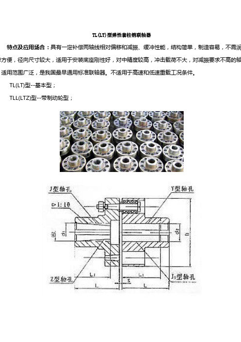
TL(LT)型弹性套柱销联轴器特点及应用场合:具有一定补偿两轴线相对偏移和减振、缓冲性能,结构简单,制造容易,不需润修方便,径向尺寸较大,适用于安装底座刚性好,对中精度较高,冲击载荷不大,对减振要求不高的轴,适用范围广泛,是我国最早通用标准联轴器。
不适用于高速和低速重载工况条件。
TL(LT)型--基本型;TLL(LTZ)型--带制动轮型;L(LT)型弹性套柱销联轴器参数及主要尺寸:(GB/T4323-84<2002>)mm2.短时过载不得超过公称扭矩值的2倍。
3.轴孔型式及长度L、L1可根据需要选取。
4.转动惯量为近似值。
ML(LM)型梅花形弹性联轴器特点及应用场合:具有补偿两轴相对偏移、减振、缓冲性能、径向尺寸小,结构简单、不用润滑、承载能力较高,维护方使、更换弹性元件需轴向移动(MLS型除外),适用于联接同轴线,起动频繁,正反转变化,中速、中等转矩传动轴系和要求工作可靠性高的工作部位。
不适用于重载、低速及轴向尺寸受艰制,更换弹性元件后两轴对中困难的部位。
ML型--基本型;MLL-II型--分体式制动轮型;MLL-I型--整体式制动轮型;MLZ型--单法兰盘;MLS型--双法兰盘;ML(LM)型梅花形弹性联轴器的参数及主要尺寸:(GB/T 5272-2002)mm型号公称扭矩Tn N.m 许用转速r/min轴孔直径d1d2dz轴孔长度LD弹性件型号转动惯量kg.m2质量kg 弹性硬件(HA)a b铁钢Y型J1Z型L推荐≥85≥94LML1 (LM1) 25 45 11500 1530012 14 32 2735 86 50MT1-a-b 0.014 0.6616 18 19 42 3020 22 24 52 38(LM2) 50 100 9500 12000 16 18 19 42 3038 95 60LM2-a-b 0.044 0.92 20 22 24 52 3825 28 62 44ML2 (LM3) 100 200 8200 10920 22 24 52 3840 103 70MT2-a-b 0.075 1.5525 28 62 4430 32 82 60ML3 (LM4) 140 280 6700 900022 24 52 3845 114 85MT3-a-b 0.178 2.525 28 62 4430 32 35 38 82 60ML4 250 400 5500 7300 25 28 62 44 50 127 105 MT4 -a 0.412 4.3HL,HLL(LX,LXZ)弹性柱销联轴器特点及应用场合:具有微量补偿性能,结构简单,容易制造,更换柱销方便,可靠性极差,适用于有轴向窜动,起动频繁,正反转的轴系传动,不适用于工作可靠性要求精度高的部位,不宜用于高速、重载及有强烈冲击振动的轴系传动,安装精度低的轴系亦不应选用。
维生素一、填充题1.维生素是维持生物体正常生长所必需的一类(微量)有机物质。
主要作用是作为(辅酶)的组分参与体内代谢。
2.根据维生素的(溶解)性质,可将维生素分为两类,即(水溶性)和(脂溶性)。
3.维生素A的活性形式是(11-顺视黄醛),可与视蛋白组成(视紫红质),后者是维持(暗)视觉所必需的。
4.维生素D在体内的主要作用是调节(钙磷)代谢,与(骨骼)生长有关。
5.维生素K的主要作用是作为(羧化酶)的辅酶。
6.维生素Bl由(嘧啶)环与(噻唑)环通过(亚甲基) 相连,主要功能是以( TPP)形式,作为( 脱羧酶 )和( 转酮酶 ) 的辅酶,转移二碳单位。
7.维生素B2的化学结构可以分为二部分,即 (二甲基异咯嗪基 ) 和( 核糖醇基 ) ,其中 (1,10位氮 ) 原子上可以加氢,因此有氧化型和还原型之分。
8.维生素B3由 (丁酸衍生物 )与 (β-丙氨酸 ) 通过 (酰胺键 ) 相连而成,组成铺酶 CoA ,作为各种酰化反应的辅酶,传递酰基。
9.维生素B5是吡啶衍生物,有烟酸,烟酰胺两种形式,其辅酶形式是 NAD+ 与 NADP+ ,作为脱氢酶的辅酶,起递氢作用。
10.维生素B6是吡啶衍生物,也称吡哆素,有吡哆醇,吡哆醛,吡哆胺三种形式,主要作为转氨酶的辅酶。
11.生物素是羧化酶的辅酶,在 CO2 的固定中起重要是作用。
12.维生素B11由蝶呤衍生物、对氨基苯甲酸、谷氨酸三部分组成,可以以四氢叶酸的形式,作为一碳单位的载体。
13.维生素B12是唯一含金属元素的维生素。
14.维生素C是羟化酶的辅酶。
二、是非题1.四种脂溶性维生素都是异戊二烯衍生物,属于类脂。
×2.B族维生素都可以作为辅酶的组分参与代谢。
√3.除了动物外,其他生物包括植物、微生物的生长也有需要维生素的现象。
√4.维生素E不容易被氧化,因此可做抗氧化剂。
×5. B族维生素具有相似的结构和生理功能。
×6.经常做日光浴有助于预防佝偻病和骨软化症的出现。
Elevate Your InspectionsFlaw DetectorEPOCH 6L TEPOCH ®6LT Portable Flaw DetectorThe EPOCH ® 6LT flaw detector combines ruggedness and ease of use in an instrument designed to be operated using only one hand, enabling fast, efficient rope access inspections and maximum uptime.Designed for Rope Access Technicians• Free Up Your Hands: Attach the instrument to your leg or harness and keep your hands free to scan for flaws and maintain balance • Comfortable: Weighs just 1.95 pounds (890 g) with a grip-oriented weight distribution for one-handed operation with minimal wrist fatigue • Easy to Use: Rotary knob and simple button design make it easy for users to navigate the menu and adjust parameters using just their thumb, even while wearing gloves• Clear, Bright Screen: Transflective 640 × 480 pixel display with outdoor mode helps make A-scans clear in difficult lighting conditions • Tough and Reliable: Engineered to IP65/67 for dust and water resistance and drop tested to protect against the hazards found in rope access inspection environmentsHarness the Power of PortabilityNo Compromises Don’t compromise on the inspection capabilities of your flaw detector. Now, inspectors who work in rope access applications can take advantage of the functionality they need in an instrument that attaches to their leg or harness for hands-free operation.Combine the EPOCH ® 6LT flaw detector with the rope access accessory kit for added functionality that helps keep rope access technicians safe during challenging inspections. The instrument fits snugly in a protective soft case that can besecurely attached to a user’s leg with the included strap or fastened to the user’s harness connection points with adjustable safety leads. However you attach it, the kit keeps the instrument in a comfortable, secure viewing position.With the unit secured, it’s easy to make parameter adjustments with one hand, leaving the other hand free to manipulate the transducer or maintain balance and personal safety. The display rotates to portrait or landscape mode for optimalA-scan viewing while the knob and buttons remain readily accessible for quick adjustments. If you’re working in a hazardous environment, add an optional screen cover for additional protection.The workflow of the EPOCH ® 6LT flaw detector is simple and straightforward. The primary screen is a large, optimized A-scan display that contains links to commonly used features and functions. Combined with an improved scanning workflow, users can complete their inspections with minimal button presses and adjustments. When you do need to navigate the menu, prominent icons make it easy to find the feature you’re looking for.Despite its small size, the EPOCH 6LT flaw detector meets the requirements of nearly any conventional ultrasonic inspectionapplication and includes additional functionality for expanded connectivity.More Functionality on the Go• Intuitive Navigation: Two-screen, icon-based interface • Optimized for One-Handed Operation: Hardware and software maximize efficient one-handed operation • Advanced Flaw Detection Capabilities: All the corefunctionality of the EPOCH 650 flaw detector and meets the requirements of EN12668-1:2010• Fast Corrosion Defect Scanning: Optional corrosion software combines the ease of a thickness gage with the flexibility of a flaw detector and includes center-pin transducer ID for faster set up • Stay Connected: Optional wireless LAN (Wi-Fi) connectivity for on-the-go data backups, setup downloads, efficient fleet management, and powerful applications through the OlympusScientific CloudRope Access Inspection Applications Powerful Corrosion and Flaw Inspection SoftwareCorrosion ModuleWith the optional corrosion module, get the best of thickness measurement and UT corrosion scanning in one instrument.Get accurate measurements from the software’s thickness measurement algorithm, true V-path correction that accounts forthe angle of dual element transducers, and ‘do zero’ that compensates for wear on the transducer’s contact plate.For speed and efficiency, the software enables the use of thickness gage transducers, making it easy to add a flaw detectorto your fleet of instruments. With automatic probe recognition, the software recognizes and automatically configures theinstrument for that probe. Likewise, when the AGC feature detects the probe’s signal, it optimizes the gain for optimalthickness measurements. Once the user begins their corrosion scanning, the grid view feature makes it easy to savethickness measurements onboard the instrument rather than having to manually record readings.Efficient Data Management• Compatible with GageView® Pro PC interface program• Export files via Wi-Fi or transfer to a removable USB memorystick• Supports bitmap (BMP), comma-separated value (CSV), andPDF file formatsConnected and Cloud EnabledThe EPOCH® 6LT flaw detector features cloud connectivity. Connect your flaw detector to the Olympus Scientific Cloud for powerful cloud-based tools, including:• Wireless firmware upgrade• File backup and archiving• Remote file access and managementCloud file management includes all EPOCH 6LT file types, as well as exported report formats and image files. This remote data sharing capability makes it easier than ever to report and communicate your inspection results.Standard Software Features• Dynamic DAC/TCG: compares echo signals to a DAC curve or reference echo• DGS/AVG: compares echo signals to a DGS/AVG diagram Added Versatility:Optional Software Features• AWS D1.1 and D1.5: Provides a dynamic indication rating for AWS inspection applications• Back Wall Echo Attenuator: Attenuates the back wall of an inspected part using the screen region defined by Gate 2Offshore Platform InspectionsWith an innovative corrosion software option and a comprehensive setof weld-related support features, corrosion scanning is fast and efficient, even while suspended above the ocean from a rope.Corrosion Module Features• Automatic probe recognition andconfiguration with center pin ID• Dynamic toggle between flaw scanning and high precision spot measurementmodes• Automatic Gain Control (AGC)• Thickness gage high precisionmeasurement algorithm• Automatic zero function (‘do zero’)• Grid view for data visualizationWeld Flaw Detectionand Sizing Features• DAC/TCG• DGS/AVG• AWS D1.1/1.5 weld rating calculator In-Service Wind TurbineInspectionWhether you’re inspecting the weldedjoints of a wind tower or compositeturbine blades, the EPOCH® 6LT flawdetector is up to the challenge.• PerfectSquare™ tunable square wavepulser• Digital high dynamic range receiver• Eight 100% digital filter sets, includinglow frequency bandwidth support• Pulser voltage up to 400 V• DAC/TCG and DGS/AVG softwarefunctionality includedBridge and StructuralSteel InspectionsThe EPOCH 6LT flaw detector offersall of the necessary features for bridgeand structural steel inspections,including an optional AWS D1.1/1.5weld rating calculator. Other featurerequirements, such as DAC/TCG andDGS/AVG, are included with everyEPOCH 6LT flaw detector.• PerfectSquare tunable square wavepulser• Digital high dynamic range pulser/receiver• Eight 100% digital filter sets• Pulser voltage from 100 V to 400 V• Five customizable digital measurementsStandard Flaw Sizing Software• DAC/TCG• DGS/AVGis certified to ISO 9001, ISO 14001, and OHSAS 18001.EPOCH ® 6LT SpecificationsGeneralUser Interface Languages English, Spanish, French, German, Japanese, Chinese, Portuguese, Russian, Italian Transducer connections LEMO 00Data storage 100,000 IDs onboardBattery type and life Single lithium-ion rechargeable standard; 6 h life Power requirements AC Mains: 100 VAC to 120 VAC, 200 VAC to 240 VAC, 50 Hz to 60 HzDisplay typeFull VGA (640 × 480 pixels) transflective color LCD, 60 Hz update rateDisplay dimensions (W × H, Diag.)117 mm × 89 mm, 146 mm (4.62 in. × 3.49 in., 5.76 in.)Overall Dimensions (W × H × D)209 mm × 128 mm × 36 mm, 58 mm at the hand grip (8.2 in. × 5 in. × 1.4 in., 2.3 in. at the hand grip)Weight890 g (1.95 lb.), including lithium-ion batteryInstrument Inputs/Outputs USB ports (1) USB 1.1 Full Speed Host (Type A)(1) USB 2.0 Full Speed Client (Type Mini B)Video output1 digital video outputEnvironmental Ratings IP ratingIngress Protection (IP) engineered to IP67 (dust tight and water submersion) and IP65 (dust tight and water jets) per IEC 60529-2004 (Degrees of Protection provided by enclosures—IP Code).Explosive atmosphere MIL-STD-810F, Method 511.4, Procedure 1.Shock tested MIL-STD-810F, Method 516.5, Procedure I, 6 cycles each axis, 15 g, 11 ms half sine.Vibration tested MIL-STD-810F, Method 514.5, Procedure I, Annex C, Figure 6, general exposure: 1 hour each axis.Operating temperature -10 °C to 50 °C (14 °F to 122 °F)Battery storage temperature 0 °C to 50 °C (32 °F to 122 °F)Pulser Pulser Tunable square wavePRF10 Hz to 2000 Hz in 10 Hz increments Energy settings 100 V, 200 V, 300 V, or 400 VPulse width Adjustable from 25 nsec to 5,000 nsec (0.1 MHz) with PerfectSquare ™ technology Damping 50, 400 ΩReceiver Gain0 to 110 dB Maximum input signal 20 Vp Receiver input impedance400 Ω ± 5%Receiver bandwidth DC to 26.5 MHz at -3 dB (standard version)0.2 to 26.5 MHz at -3 dB (EN12668 compliant version)Digital filter settings8 digital filter sets (standard version)7 digital filter sets (EN12668 compliant version)Rectification Full-Wave, Positive Half-Wave, Negative Half-Wave, RF System linearity Horizontal: ± 0.5% FSWResolution 0.25% FSH, amplifier accuracy ± 1dB Reject0 to 85% FSH in 1% increment positions Amplitude measurement 1.25% to 110% full screen heightMeasurement rate Equivalent to PRF in all modes (single shot)CalibrationAutomated calibrationVelocity, zero offsetStraight beam (first back wall or echo-to-echo)Angle beam (sound path or depth)Test modes Pulse echo, dual, or through transmission Units Millimeters, inches, or microsecondsRange 4.31 mm to 6,700 mm at 5,900 m/s (0.2320 in./μs)Velocity 635 m/s to 15240 m/s (0.0250 in./μs to 0.6000 in./μs)Zero offset 0 to 750 μsDisplay delay -10 microseconds to 2203 microseconds Refracted angle 0° to 85° in 0.1° increments, then jump to 90°GatesMeasurement gates 2 fully independent flaw gates Gate start Variable over entire displayed rangeGate width Variable from 0.040 microseconds to end of displayed rangeGate heightVariable from 2 to 95% full screen height in 1% incrementsAlarmsPositive and negative threshold/curve, minimum depth (gate 1 and gate 2)MeasurementsMeasurement display locations 5 locations available (manual or auto selection)Gate (1, 2)Thickness, sound path, projection, depth, amplitude, time-of-flight, min./max. depth, min./max. amplitude, sizing measurements based on mode Echo-to-echo Standard gate 2 – gate 1DAC/TCGStandard, up to 50 points, 110 dB dynamic TCG rangeSpecial DAC modes Custom DAC (up to 6 curves), 20–80% view Curved surface correctionStandard OD or bar correction for angle beam measurementsSoftware OptionsEP6LT-AWS (Q1400007):AWS D1.1/D1.5 weld rating calculatorEP6LT-CORRSN (Q1400008): Corrosion moduleEP6LT-BEA (Q1400009): Back wall echo attenuation gateOptional AccessoriesBATT-10025-0024 (Q7600001): Lithium-ion rechargeable battery EP-MCA-X :EPOCH series charger / adaptor with power cordHNDL-10018-0001 (Q7790068): EPOCH 6LT wrist strapEPLTC-C-USB-A-6 (U8840031): USB cable, mini A to mini BCASE-10042-0001 (Q7640003): EPOCH 6LT transport case 600-DP (U8780297):Display protectors (10 pack)EP6LT-KIT-ROPE (Q7790069): EPOCH 6LT rope access accessory kitEP4/CH (U8140055):EPOCH series chest harness EP6LT-STAND (Q7790070): EPOCH 6LT desktop stand EPXT-EC-x :EPOCH series external charging base with power cord。
LT-6型双温蒸汽挂烫机
LT-6型此款属于08新款,在原有LT-6型技术基础上进行改良,外型更加美观,属于当今最流行的大小轮款式,内部结构更加合理。
内部采用电子控温技术。
他有两个大小不同的蒸汽可以选择。
主要有以下几方面特点:1、产品颜色(1、富贵红 2、柠檬黄 3、嫩草绿 4、太白银);2、可拆卸水晶毛刷;3、伸缩型4节不锈钢挂杆;4、插入式气路连接装置; 5、底部万向轮结构,移动自如; 6、全透明水晶水壶;7、双温开关调温; 8、水壶自动供水装置;9、不锈钢喷头;10、折叠衣架;11、裤缝夹;
12、橡胶防滑手柄
LT-6型双温蒸汽挂烫机技术参数。